EP1096551A2 - Method for making integrated circuits having features with reduced critical dimensions - Google Patents
Method for making integrated circuits having features with reduced critical dimensions Download PDFInfo
- Publication number
- EP1096551A2 EP1096551A2 EP00309101A EP00309101A EP1096551A2 EP 1096551 A2 EP1096551 A2 EP 1096551A2 EP 00309101 A EP00309101 A EP 00309101A EP 00309101 A EP00309101 A EP 00309101A EP 1096551 A2 EP1096551 A2 EP 1096551A2
- Authority
- EP
- European Patent Office
- Prior art keywords
- layer
- photoresist
- aluminum
- forming
- features
- Prior art date
- Legal status (The legal status is an assumption and is not a legal conclusion. Google has not performed a legal analysis and makes no representation as to the accuracy of the status listed.)
- Withdrawn
Links
Images

Classifications
-
- H—ELECTRICITY
- H10—SEMICONDUCTOR DEVICES; ELECTRIC SOLID-STATE DEVICES NOT OTHERWISE PROVIDED FOR
- H10W—GENERIC PACKAGES, INTERCONNECTIONS, CONNECTORS OR OTHER CONSTRUCTIONAL DETAILS OF DEVICES COVERED BY CLASS H10
- H10W20/00—Interconnections in chips, wafers or substrates
- H10W20/01—Manufacture or treatment
- H10W20/031—Manufacture or treatment of conductive parts of the interconnections
-
- G—PHYSICS
- G03—PHOTOGRAPHY; CINEMATOGRAPHY; ANALOGOUS TECHNIQUES USING WAVES OTHER THAN OPTICAL WAVES; ELECTROGRAPHY; HOLOGRAPHY
- G03F—PHOTOMECHANICAL PRODUCTION OF TEXTURED OR PATTERNED SURFACES, e.g. FOR PRINTING, FOR PROCESSING OF SEMICONDUCTOR DEVICES; MATERIALS THEREFOR; ORIGINALS THEREFOR; APPARATUS SPECIALLY ADAPTED THEREFOR
- G03F7/00—Photomechanical, e.g. photolithographic, production of textured or patterned surfaces, e.g. printing surfaces; Materials therefor, e.g. comprising photoresists; Apparatus specially adapted therefor
- G03F7/004—Photosensitive materials
- G03F7/09—Photosensitive materials characterised by structural details, e.g. supports, auxiliary layers
- G03F7/11—Photosensitive materials characterised by structural details, e.g. supports, auxiliary layers having cover layers or intermediate layers, e.g. subbing layers
-
- H—ELECTRICITY
- H10—SEMICONDUCTOR DEVICES; ELECTRIC SOLID-STATE DEVICES NOT OTHERWISE PROVIDED FOR
- H10P—GENERIC PROCESSES OR APPARATUS FOR THE MANUFACTURE OR TREATMENT OF DEVICES COVERED BY CLASS H10
- H10P50/00—Etching of wafers, substrates or parts of devices
- H10P50/71—Etching of wafers, substrates or parts of devices using masks for conductive or resistive materials
-
- H—ELECTRICITY
- H10—SEMICONDUCTOR DEVICES; ELECTRIC SOLID-STATE DEVICES NOT OTHERWISE PROVIDED FOR
- H10P—GENERIC PROCESSES OR APPARATUS FOR THE MANUFACTURE OR TREATMENT OF DEVICES COVERED BY CLASS H10
- H10P76/00—Manufacture or treatment of masks on semiconductor bodies, e.g. by lithography or photolithography
- H10P76/20—Manufacture or treatment of masks on semiconductor bodies, e.g. by lithography or photolithography of masks comprising organic materials
- H10P76/204—Manufacture or treatment of masks on semiconductor bodies, e.g. by lithography or photolithography of masks comprising organic materials of organic photoresist masks
- H10P76/2041—Photolithographic processes
Definitions
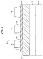
- Another step includes exposing the photoresist layer to a pattern image (Block 42 ).
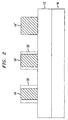
- a following step includes developing the exposed photoresist layer using a developer and stripping away undeveloped portions (Block 44 ) to define remaining photoresist portions having reduced widths adjacent the aluminum layer based upon an interaction between the photoresist, the developer and the aluminum.
- An example of a preferred developer for use with the method of the present invention is Shipley's MF505.
Landscapes
- Engineering & Computer Science (AREA)
- Architecture (AREA)
- Structural Engineering (AREA)
- Physics & Mathematics (AREA)
- General Physics & Mathematics (AREA)
- Photosensitive Polymer And Photoresist Processing (AREA)
- Internal Circuitry In Semiconductor Integrated Circuit Devices (AREA)
- Drying Of Semiconductors (AREA)
- Exposure Of Semiconductors, Excluding Electron Or Ion Beam Exposure (AREA)
Abstract
Description

Claims (18)
- A method for making an integrated circuit comprising the steps of:forming an aluminum layer adjacent a semiconductor wafer;forming a photoresist layer adjacent the aluminum layer, with at least a portion of the aluminum layer being uncovered;exposing the photoresist layer to a pattern image;developing the exposed photoresist layer using a developer and stripping away undeveloped photoresist portions to define a mask including mask features having reduced widths than would otherwise be produced adjacent the aluminum layer and based upon an interaction between the photoresist, the developer and the aluminum; andetching the aluminum layer using the mask including features having the reduced widths to thereby define circuit features having a smaller critical dimension than would otherwise be produced.
- A method according to claim 1, wherein the etched aluminum layer defines an interconnect level for the integrated circuit.
- A method according to claim 1, further comprising the step of forming a dielectric layer adjacent the semiconductor wafer, and wherein the aluminum layer is formed on the dielectric layer.
- A method for making an integrated circuit comprising the steps of:forming a metal layer adjacent a semiconductor wafer;forming a positive photoresist layer adjacent the metal layer, with at least a portion of the metal layer being uncovered;exposing the photoresist layer to a pattern image;developing the exposed photoresist layer using a developer and stripping away undeveloped photoresist portions to define a mask including mask features having reduced widths than would otherwise be produced adjacent the metal layer and based upon an interaction between the photoresist, the developer and the metal; andetching the metal layer using the mask including mask features having the reduced widths to thereby define circuit features having a smaller critical dimension than would otherwise be produced.
- A method according to claim 1 or 4, further comprising the step of designing a reticle to form the pattern image to account for the reduced widths of the mask features.
- A method according to claim 4, wherein the metal comprises aluminum.
- A method according to claim 4, wherein the remaining photoresist portions define profiles with substantially vertical sidewalls.
- A method according to claim 4, further comprising the step of forming an antireflective layer on the metal layer prior to the step of forming the photoresist layer.
- A method according to claim 4, wherein the positive photoresist comprises a photosensitive compound, a base resin, and an organic solvent.
- A method according to claim 4, wherein the etched metal layer defines an interconnect level for the integrated circuit.
- A method according to claim 4, further comprising the step of forming a dielectric layer adjacent the semiconductor wafer, arid wherein the metal layer is formed on the dielectric layer.
- A method for making an integrated circuit comprising the steps of:forming a dielectric layer adjacent a semiconductor wafer;forming an aluminum layer adjacent the dielectric layer;forming a photoresist layer adjacent the aluminum layer with at least a portion of the aluminum layer being uncovered;exposing the photoresist layer to a pattern image;developing the exposed photoresist layer using a developer and stripping away undeveloped photoresist portions to define a mask including mask features having reduced widths than would otherwise be produced adjacent the aluminum layer and based upon an interaction between the photoresist, the developer and the aluminum; andetching the aluminum layer using the mask including features having the reduced widths to thereby define circuit features having a smaller critical dimension than would otherwise be produced.
- A method according to claim 12, further comprising the step of designing a reticle to form the pattern image to account for the reduced widths of the remaining photoresist portions.
- A method according to claim 1 or 12, wherein the mask features define profiles with substantially vertical sidewalls.
- A method according to claim 1 or 12, further comprising the step of forming an antireflective layer on the aluminum layer prior to the step of forming the photoresist layer.
- A method according to claim 1 or 15, wherein the antireflective layer comprises a refractory metal nitride.
- A method according to claim 1, 4 or 12, further comprising the step of removing the mask after the etching step.
- A method according to claim 1 or 12, wherein the photoresist is a positive photoresist comprising a photosensitive compound, a base resin, and an organic solvent.
Applications Claiming Priority (2)
| Application Number | Priority Date | Filing Date | Title |
|---|---|---|---|
| US430147 | 1982-09-30 | ||
| US09/430,147 US6294465B1 (en) | 1999-10-29 | 1999-10-29 | Method for making integrated circuits having features with reduced critical dimensions |
Publications (2)
| Publication Number | Publication Date |
|---|---|
| EP1096551A2 true EP1096551A2 (en) | 2001-05-02 |
| EP1096551A3 EP1096551A3 (en) | 2002-01-09 |
Family
ID=23706256
Family Applications (1)
| Application Number | Title | Priority Date | Filing Date |
|---|---|---|---|
| EP00309101A Withdrawn EP1096551A3 (en) | 1999-10-29 | 2000-10-16 | Method for making integrated circuits having features with reduced critical dimensions |
Country Status (4)
| Country | Link |
|---|---|
| US (1) | US6294465B1 (en) |
| EP (1) | EP1096551A3 (en) |
| JP (1) | JP2001185482A (en) |
| KR (1) | KR20010051264A (en) |
Families Citing this family (3)
| Publication number | Priority date | Publication date | Assignee | Title |
|---|---|---|---|---|
| US7033929B1 (en) * | 2002-12-23 | 2006-04-25 | Lsi Logic Corporation | Dual damascene interconnect structure with improved electro migration lifetimes |
| US7261745B2 (en) * | 2003-09-30 | 2007-08-28 | Agere Systems Inc. | Real-time gate etch critical dimension control by oxygen monitoring |
| US8945808B2 (en) * | 2006-04-28 | 2015-02-03 | International Business Machines Corporation | Self-topcoating resist for photolithography |
Family Cites Families (9)
| Publication number | Priority date | Publication date | Assignee | Title |
|---|---|---|---|---|
| JP2504832B2 (en) * | 1989-06-16 | 1996-06-05 | シャープ株式会社 | Method of forming resist pattern |
| US5397433A (en) * | 1993-08-20 | 1995-03-14 | Vlsi Technology, Inc. | Method and apparatus for patterning a metal layer |
| KR100346448B1 (en) * | 1994-12-29 | 2002-11-23 | 주식회사 하이닉스반도체 | Exposure mask for semiconductor device |
| US5525542A (en) * | 1995-02-24 | 1996-06-11 | Motorola, Inc. | Method for making a semiconductor device having anti-reflective coating |
| JP3409493B2 (en) * | 1995-03-13 | 2003-05-26 | ソニー株式会社 | Mask pattern correction method and correction device |
| US5856241A (en) * | 1995-07-26 | 1999-01-05 | Kabushiki Kaisha Toshiba | Method of manufacturing semiconductor device |
| US5841179A (en) * | 1996-08-28 | 1998-11-24 | Advanced Micro Devices, Inc. | Conductive layer with anti-reflective surface portion |
| US5846878A (en) * | 1997-02-28 | 1998-12-08 | Nec Corporation | Method of manufacturing a wiring layer in a semiconductor device |
| US5915203A (en) * | 1997-06-10 | 1999-06-22 | Vlsi Technology, Inc. | Method for producing deep submicron interconnect vias |
-
1999
- 1999-10-29 US US09/430,147 patent/US6294465B1/en not_active Expired - Lifetime
-
2000
- 2000-10-16 EP EP00309101A patent/EP1096551A3/en not_active Withdrawn
- 2000-10-26 KR KR1020000063209A patent/KR20010051264A/en not_active Withdrawn
- 2000-10-27 JP JP2000328361A patent/JP2001185482A/en active Pending
Also Published As
| Publication number | Publication date |
|---|---|
| EP1096551A3 (en) | 2002-01-09 |
| KR20010051264A (en) | 2001-06-25 |
| JP2001185482A (en) | 2001-07-06 |
| US6294465B1 (en) | 2001-09-25 |
Similar Documents
| Publication | Publication Date | Title |
|---|---|---|
| US8148052B2 (en) | Double patterning for lithography to increase feature spatial density | |
| US6475867B1 (en) | Method of forming integrated circuit features by oxidation of titanium hard mask | |
| US6197687B1 (en) | Method of patterning field dielectric regions in a semiconductor device | |
| US20220077136A1 (en) | Method for fabricating semiconductor structure with strengthened patterns | |
| US20080203518A1 (en) | Method for positioning sub-resolution assist features | |
| US8698206B2 (en) | Feature patterning methods and structures thereof | |
| US20030213968A1 (en) | Imageable bottom anti-reflective coating for high resolution ligthography | |
| KR100295426B1 (en) | Wiring forming method | |
| US6660456B2 (en) | Technique for the size reduction of vias and other images in semiconductor chips | |
| US6294465B1 (en) | Method for making integrated circuits having features with reduced critical dimensions | |
| US6613500B1 (en) | Reducing resist residue defects in open area on patterned wafer using trim mask | |
| US6620564B2 (en) | Method for patterning semiconductors through adjustment of image peak side lobes | |
| JPH09190959A (en) | Method of forming resist pattern | |
| US20040171275A1 (en) | Semiconductor device and a fabrication method thereof | |
| US20070099424A1 (en) | Reduction of mechanical stress on pattern specific geometries during etch using double pattern layout and process approach | |
| US6686129B2 (en) | Partial photoresist etching | |
| US20030201543A1 (en) | Deep UV-resistant photoresist plug for via hole | |
| CN1279607C (en) | Method for forming pad oxide layer in semiconductor integrated circuit | |
| US6316340B1 (en) | Photolithographic process for preventing corner rounding | |
| JP2001155994A (en) | Method for manufacturing integrated circuits including components having relatively small critical dimensions | |
| US20070178409A1 (en) | Exposure method of forming three-dimensional lithographic pattern | |
| US20070178410A1 (en) | Method of forming three-dimensional lithographic pattern | |
| KR20040095159A (en) | Method of forming resist pattern and method of manufacturing semiconductor device | |
| KR100333389B1 (en) | Method of manufacturing contact hole of semiconductor device | |
| US20060040216A1 (en) | Method of patterning photoresist film |
Legal Events
| Date | Code | Title | Description |
|---|---|---|---|
| PUAI | Public reference made under article 153(3) epc to a published international application that has entered the european phase |
Free format text: ORIGINAL CODE: 0009012 |
|
| AK | Designated contracting states |
Kind code of ref document: A2 Designated state(s): AT BE CH CY DE DK ES FI FR GB GR IE IT LI LU MC NL PT SE |
|
| AX | Request for extension of the european patent |
Free format text: AL;LT;LV;MK;RO;SI |
|
| PUAL | Search report despatched |
Free format text: ORIGINAL CODE: 0009013 |
|
| AK | Designated contracting states |
Kind code of ref document: A3 Designated state(s): AT BE CH CY DE DK ES FI FR GB GR IE IT LI LU MC NL PT SE |
|
| AX | Request for extension of the european patent |
Free format text: AL;LT;LV;MK;RO;SI |
|
| RIC1 | Information provided on ipc code assigned before grant |
Free format text: 7H 01L 21/027 A, 7H 01L 21/3213 B |
|
| AKX | Designation fees paid | ||
| REG | Reference to a national code |
Ref country code: DE Ref legal event code: 8566 |
|
| STAA | Information on the status of an ep patent application or granted ep patent |
Free format text: STATUS: THE APPLICATION IS DEEMED TO BE WITHDRAWN |
|
| 18D | Application deemed to be withdrawn |
Effective date: 20020710 |