EP1096532A1 - Electron emission device - Google Patents
Electron emission device Download PDFInfo
- Publication number
- EP1096532A1 EP1096532A1 EP00123265A EP00123265A EP1096532A1 EP 1096532 A1 EP1096532 A1 EP 1096532A1 EP 00123265 A EP00123265 A EP 00123265A EP 00123265 A EP00123265 A EP 00123265A EP 1096532 A1 EP1096532 A1 EP 1096532A1
- Authority
- EP
- European Patent Office
- Prior art keywords
- electron emission
- semiconductor layer
- porosity
- thin
- emission device
- Prior art date
- Legal status (The legal status is an assumption and is not a legal conclusion. Google has not performed a legal analysis and makes no representation as to the accuracy of the status listed.)
- Granted
Links
Images

Classifications
-
- B—PERFORMING OPERATIONS; TRANSPORTING
- B82—NANOTECHNOLOGY
- B82Y—SPECIFIC USES OR APPLICATIONS OF NANOSTRUCTURES; MEASUREMENT OR ANALYSIS OF NANOSTRUCTURES; MANUFACTURE OR TREATMENT OF NANOSTRUCTURES
- B82Y10/00—Nanotechnology for information processing, storage or transmission, e.g. quantum computing or single electron logic
-
- H—ELECTRICITY
- H01—ELECTRIC ELEMENTS
- H01J—ELECTRIC DISCHARGE TUBES OR DISCHARGE LAMPS
- H01J1/00—Details of electrodes, of magnetic control means, of screens, or of the mounting or spacing thereof, common to two or more basic types of discharge tubes or lamps
- H01J1/02—Main electrodes
- H01J1/30—Cold cathodes, e.g. field-emissive cathode
- H01J1/312—Cold cathodes, e.g. field-emissive cathode having an electric field perpendicular to the surface, e.g. tunnel-effect cathodes of metal-insulator-metal [MIM] type
Definitions
- the present invention relates to an electron emission device and particularly to a porous semiconductor electron emission device.
- an Field Emission Display In field electron emission display apparatuses, an Field Emission Display (FED) is known as a planar emission display device equipped with an array of cold-cathode electron emission source which does not require cathode heating.
- FED Field Emission Display
- planar electron sources such as an electron emission device with a metal-insulator-metal (MIM) structure and to an electron emission device using a porous semiconductor such as silicon (Si).
- the porous semiconductor electron emission device comprises a porous semiconductor layer and a thin-film metal electrode both are formed in turn on a silicon layer provided with an ohmic electrode at the back side. If the porous semiconductor electron emission device is used for a display device, a part of electrons are passed through the thin-film metal electrode by a voltage applied across the thin-film metal electrode and the silicon layer so that the electrons travelling a vacuum space impinge on a facing electrode covered with a fluorescent material to emit light.
- the electron emission device with the MIM structure or porous semiconductor electron emission device does not yet provide a sufficient amount of emitted electrons.
- the present invention has been made to solve such a problem in view of the forgoing status. Therefore an object of the present invention to provide an electron emission device with a high electron emission efficiency.
- An electron emission device comprises:
- said thin-film metal electrode and said carbon region are deposited through a physical deposition method or a chemical deposition method.
- said carbon region is a thin film deposited on said thin-film metal electrode.
- said carbon region is distributed within said thin-film metal electrode.
- said carbon region is a thin film deposited under said thin-film metal electrode.
- the porous semiconductor layer is formed by an anodization processing to the surface of the semiconductor layer to be made as a porous portion.
- the porous semiconductor layer has at least two or more of porosity-changed layers which have porosities which are different from each other in the thickness direction.
- the porosity-changed layer with a high porosity and another porosity-changed layer with a low porosity are layered by turns in the thickness direction of the porous semiconductor layer.
- the semiconductor layer is anodic-oxidized from the surface thereof in such a manner that a first processing time duration in which a low current density for the anodization processing is applied to the surface and a second processing time duration in which a high current density for the anodization processing is applied to the surface are repeated by turns, so that the porosity-changed layer with a high porosity and another porosity-changed layer with a low porosity are layered by turns in the thickness direction of the porous semiconductor layer.
- the porosity-changed layers have incline porosity ascended gradually in the thickness direction.
- the porosity-changed layers have incline porosity descended gradually in the thickness direction.
- the semiconductor layer is anodic-oxidized from the surface thereof during a processing time in which a current density for the anodization processing is changed so that the porosity-changed layers have incline porosities in the thickness direction.
- this electron emission device when in use in a display device, can provide a high luminance, can suppress the consumption of the driving electric current and the generation of heat from the device, and can reduce a load on the driving circuit for the display device.
- This electron emission device is a plane or dot electron emission diode which can serve as a light-emitting diode or a laser diode which emits electromagnetic waves of infrared rays, visible light or ultraviolet rays.
- the electron emission device of the invention since the porous surface of the porous semiconductor layer becomes a smoothed flat and the contact area with the surface of the thin-film metal electrode increases, the electron emission is stabilized. In addition, since a high density layer with a low porosity exists in the inside of the porous semiconductor layer, the rate of thermal conductivity increases in the layer and the thermal destruction of device comes to seldom occur due to a heat-dissipation effect.
- the electron emission device using a porous semiconductor layer embodying the present invention comprises a porous semiconductor layer 13, a thin-film metal electrode 15 and a carbon region or thin film made of carbon or a carbon compound 40 which are formed in turn on a silicon layer 12 provided with an ohmic electrode 11 at the back side.
- the porous semiconductor layer 13 is formed by an anodic oxidation of the Si semiconductor layer 12 after the formation thereof.
- the porous semiconductor layer 13 has a thickness ranging of from 1 to 50 micrometers.
- forms of carbon such as amorphous carbon, graphite, carbyne, fullerene (C 2n ), diamond-like carbon, carbon nano-tube, and diamond etc., or carbon compounds such as ZrC, SiC, WC, and MoC etc. are effective.
- the physical methods are known as physical vapor deposition (PVD) and include a vacuum deposition method, molecular beam epitaxy method, sputtering method, ionized vapor deposition method and laser abrasion method.
- the chemical methods are known as chemical vapor deposition (CVD) and include thermal CVD, plasma CVD and MOCVD (metal-organic chemical vapor deposition) etc. Among these methods, the sputtering method is especially effective.
- the carbon regions may be provided as a thin-film metal electrode 15a by having them distributed within the thin-film metal electrode.
- the formation process of the carbon region is performed as the thin-film metal electrode formation process in which the thin-film metal electrode 15a containing the carbon region is formed over the porous semiconductor layer 13, with carbon or a carbon compound being mixed with the metal by using i.e. a mixed target or by sputtering within a carbon or carbon compound gas atmosphere.
- the carbon region 40 may be formed as a thin film deposited under the thin-film metal electrode 15 as shown in Fig. 3.
- the forming process of the carbon region is performed after the formation process of the porous semiconductor layer 13, followed by the formation process of the thin-film metal electrode 15 over the carbon region 40.
- the formation process of the carbon region is performed immediately before the formation process of the thin-film metal electrode 15.
- the structure shown in Fig. 3 is obtained in which the carbon region 40 is formed between the thin-film metal electrode 15 and the porous semiconductor layer 13.
- the porous semiconductor electron emission device can be regarded as a diode of which the thin-film metal electrode 15 at its surface is connected to a positive potential Vps and the back, i.e., ohmic electrode 11 is connected to a ground potential.
- Vps positive potential
- Ips diode current
- the porous semiconductor layer 13 has a high resistance
- most of the applied electric field is applied to the porous semiconductor layer 13.
- the electrons travel inside the porous semiconductor layer 13 toward the thin-film metal electrode 15. Some of the electrons that reach near the thin-film metal electrode 15 pass through the thin-film metal electrode 15, due to the strong electric field, to be discharged out into a vacuum space 4 if the vacuum space exists in the outside.
- the device substrate provided with the porous semiconductor electron emission devices is used as the first substrate at the backside, and a transparent second substrate 1 such as one made of glass is retained as the front side substrate via a vacuum space 4 as shown in Fig. 1.
- a transparent collector electrode 2 made of indium-tin oxide (what we call ITO), tin oxide (SnO) or zinc oxide (ZnO) etc. and a phosphor layer of R, G or B are formed in turn.
- the collector electrodes 2 capturing emitted electrons are grouped per three for R, G and B color signals corresponding to Red, Green and Blue emitting portions.
- fluorescent material layers 3R, 3G and 3B corresponding to R, G and B emissions are formed on the corresponding collector electrodes 2.
- the electrons e (emission current Iem) discharged from the carbon region 40 are accelerated by a high voltage Vc which is applied to the opposing collector electrode (transparent electrode) 2, and are collected at the electrode 2.
- the fluorescent material layers coated on the collector electrode 2 emit corresponding visible luminous energy.
- Fig. 4 shows another embodiment of the present invention which is the same as the above embodiment comprising the ohmic electrode 11, the semiconductor layer 12 and the thin-film metal electrode 15, except that the porous semiconductor layer 13 consists of at least two or more of porosity-changed layers 13a and 13b which have porosities different from each other respectively in the thickness direction.
- the porous semiconductor layer 13 is formed so that a porosity-changed layer with a high porosity 13a and a porosity-changed layer with a low porosity 13b may be alternately layered by in the thickness direction.
- the porosity-changed layer with a high porosity 13a thus has an electrical resistance lower than that of the porosity-changed layer with a low porosity 13b.
- the high porosity-changed layer 13a and/or low porosity-changed layer 13b may be formed in such a manner that each may have an incline porosity gradually ascended in the thickness direction.
- the incline porosity may be gradually descended in the thickness direction.
- the porosity-changed layer with a low porosity 13b having a high resistance should be flatly formed on the outer-most surface.
- the low porosity-changed layer 13b prevents a superfluous current of the diode current Ips, and improves the contact with the thin-film metal electrode 15 formed thereon.
- the porosity-changed layer with a low porosity 13b is layered by turns, the thermal dissipation of the device will be promoted.
- the electron emission device emits electrons although the thin-film electrode of metal such as Pt is simply prepared on the low porosity-changed layer 13b.
- oxidization or nitriding may be performed on the resulted porous semiconductor layer under the following conditions and, after that, the thin-film electrode of metal such as Pt is prepared, so that an emission stability and durability of the device are improved more.
- the porous semiconductor layer may be oxidized under the oxidization conditions of a temperature ranging from 700 to 1200 degrees Centigrade and a time period of form 1 to 120 minutes in oxygen gas, alternatively under the oxidization conditions of a temperature ranging from 200 to 900 degrees Centigrade and a time period of form 1 to 120 minutes in oxygen plasma.
- the porous semiconductor layer may be nitrided under the nitriding conditions of a temperature ranging from 700 to 1200 degrees Centigrade and a time period of form 1 to 120 minutes in nitrogen gas, alternatively under the nitriding conditions of a temperature ranging from 200 to 900 degrees Centigrade and a time period of form 1 to 120 minutes in nitrogen plasma.
- a Si wafer of a single-crystalline, amorphous, poly-crystalline, n-type or p-type may be used for a device-substrate in which the porous Si layer is formed through the anodization.
- the thin Si layer may be deposited on the ohmic electrodes previously formed on a substrate. This case is convenient to a display device comprising a plurality of electron emission devices.
- vacuum deposition method is particularly effective in forming those layers and the substrate
- CVD Chemical Vapor Deposition
- laser ablation method is particularly effective in forming those layers and the substrate
- MBE Molecular Beam Epitaxy
- ion beam sputtering is particularly effective.
- the material of the semiconductor layer 12 preferably used is silicon (Si), but not restricted in the present invention.
- silicon silicon
- the crystal substrate having its surface (100) direction orientating perpendicular to its major surface is preferably used, because the electron emission efficiency ⁇ of the porous Si layer is better.
- the porous semiconductor layer 13 is formed in the semiconductor wafer 12 through the anodic treatment.
- a semiconductor wafer 12 of an n-type Si is preformed by an anodic treatment, in which an insulative layer with a rectangle opening is previously formed on the semiconductor wafer.
- the semiconductor wafer is then dipped into a hydrogen fluoride (HF) solution bath.
- HF hydrogen fluoride
- the surface of the semiconductor layer is partially exposed in the HF solution through the opening of the insulative layer.
- the exposed semiconductor layer as an anode and the cathode of Pt are disposed facing to each other in the HF solution.
- the anode and cathode are connected to a DC power supply, so that a DC current is applied across these electrodes with a low current density to anodize the exposed semiconductor layer.
- a p-type porous Si layer is formed in the Si substrate.
- the formation of the porous structure requires the consumption of positive holes and thus the light-irradiation should be preformed during the anodization to supply the positive hole carriers to the exposed semiconductor layer.
- the porous Si layer may be formed on a p-type Si semiconductor layer. In this case, the porous Si layer may be formed even if it is in a dark condition.
- the porous Si layer is consisted of plural minute channels or open spaces and the residual Si .
- the pore channel's diameter is in a range from approximately one to several hundreds nano-meters and the dimension of each residual Si skeleton is in a range from the number of tens to hundreds of Si atoms, it is expected that an electron emission phenomenon occurs due to the quantum size effect.
- These values may be controlled by the settings of the conditions of the HF density, the current density, the duration of anodization treatment and the light-irradiation time period during the anodic treatment.
- the porosity is changed at 10 to 80% in the thickness direction of the porous semiconductor layer 13 having the porosity-changed layers 13a and 13b.
- This change of porosity is preformed in each porosity-changed layer.
- the porosity-changed layers 13a and 13b formed by turns in such a manner that anodizations both of the short processing period with a low current density and of the long processing period with a high current density are repeated by turns, as shown in Figs.
- the long processing periods with a high current density are equal to each other for forming the porosity-changed layers with a high porosity 13a intermittently, as shown in Fig. 5A.
- the long processing periods with a high current density may be gradually made short for forming the high porosity-changed layers 13a becoming thin gradually, as shown in Fig. 5B.
- the porosity-changed layers each having a porosity different from the contiguities in the thickness direction can also be formed in the porous semiconductor layer by means of anodizations under the conditions of the current densities and the processing periods as shown in Figs. 6C and 6D.
- the specific resistance becomes small so that it is close to the Si layer 12 in each layer.
- the current density is gradually changed during the anodization.
- the porous Si layer 13 may have a high resistivity at a portion adjacent to its surface and a low resistivity at a portion adjacent to its interface between the porous Si layer 13 and the Si substrate 12. This continuous incline of resistivity in the porous Si layer 13 is preferable for the injection of electrons from the substrate.
- metals such as Pt, Au, W, Ru and Ir are effective as the material for the thin-film metal electrode 15 on the electron emission side, Al, Sc, Ti, V, Cr, Mn, Fe, Co, Ni, Cu, Zn, Ga, Y, Zr, Nb, Mo, Tc, Rh, Pd, Ag, Cd, Ln, Sn, Ta, Re, Os, Tl, Pb, La, Ce, Pr, Nd, Pm, Sm, Eu, Gd, Tb, Dy, Ho, Er, Tm, Yb, Lu and an alloy of individuals thereof can be used as well. From the principle of electron emission, it is better that the material for the thin-film metal electrode 15 has a lower work function ⁇ and is thinner.
- the material for the thin-film metal electrode 15 should be a metal of the group I or group II in the periodic table; for example, Cs, Rb, Li, Sr, Mg, Ba, Ca and the like are effective and alloys of those elements may be used as well.
- the material for the thin-film metal electrode 15 should be a chemically stable metal with a high conductivity; for example, single substances of Au, Pt, Lu, Ag and Cu or alloys thereof are desirable. It is effective to coat or dope a metal with a low work function as described above on or in those metals. Utilizable efficiency is obtained by using an Au or Pt thin-film electrode having a thickness of from 1 to 50 nm. When considering the stability as an electron emission device, a thickness of from 2 to 20 nm is the most suitable for the Au or Pt thin-film electrode.
- the material for the ohmic electrodes 11 is Au, Pt, Al, W or the like which is generally used for the wires of an IC, and has a uniform thickness for supplying substantially the same current to the individual devices.
- the material for another device-substrate (not shown) on which the semiconductor Si layer 12 is deposited as a thin-film may be ceramics such as Al 2 O 3 , Si 3 N 4 or BN instead of glass.
- the electron emission devices were produced from Si wafers of 14mm x 14mm, and their characteristic were investigated.
- the same electron emission device was produced as comparative examples in such a manner as the above-mentioned case except having a conventional porous silicon layer with a uniform porosity. At this case, it carried out under the following anodization conditions.
- a 6 mm diameter thin-film metal electrode of Pt was formed 6 nm thick on the surface of the amorphous SiO 2 layer of each substrate by sputtering, thus providing a plurality of device-substrates.
- transparent substrates were prepared, each of which has a collector electrode of indium tin oxide (ITO) formed inside a transparent glass substrate and has a fluorescent layer of a fluorescent substance corresponding to R, G or B color emission formed on the collector electrode by the normal scheme.
- ITO indium tin oxide
- Electron emission devices were assembled in each of which the device-substrate and the transparent substrate are supported apart from one another by 10 mm in parallel by a spacer in such a way that the thin-film metal electrode 15 faced the collector electrode 2, with the clearance therebetween made to a vacuum of 10-5 Pa.
- the diode current Ips and the emission current Iem corresponding to the thickness of the SiO 2 film of each of the acquired plural devices were measured.
- the uniform electron emission is caused by the porous semiconductor layer having at least two or more of porosity-changed layers which have porosities which are different from each other in the thickness direction and the emission exhibits a high linearity, and that those devices can serve as an electron emission diode, or a light-emitting diode or laser diode which emits electromagnetic waves of infrared rays, visible light or ultraviolet rays.
- the present invention eliminates the problem of the contact between the porous semiconductor layer and the thin-film metal electrode formed thereon to make the electron emission stable. Such a contact problem is caused by a phenomenon that the rough surface of the porous semiconductor layer after the anodic oxidation prevents from contacting closely with the thin-film metal electrode.
Landscapes
- Engineering & Computer Science (AREA)
- Chemical & Material Sciences (AREA)
- Nanotechnology (AREA)
- Physics & Mathematics (AREA)
- Mathematical Physics (AREA)
- Theoretical Computer Science (AREA)
- Crystallography & Structural Chemistry (AREA)
- Cold Cathode And The Manufacture (AREA)
- Cathode-Ray Tubes And Fluorescent Screens For Display (AREA)
- Electrodes For Cathode-Ray Tubes (AREA)
Abstract
Description
- The present invention relates to an electron emission device and particularly to a porous semiconductor electron emission device.
- In field electron emission display apparatuses, an Field Emission Display (FED) is known as a planar emission display device equipped with an array of cold-cathode electron emission source which does not require cathode heating. There also exists attentions to planar electron sources such as an electron emission device with a metal-insulator-metal (MIM) structure and to an electron emission device using a porous semiconductor such as silicon (Si).
- The porous semiconductor electron emission device comprises a porous semiconductor layer and a thin-film metal electrode both are formed in turn on a silicon layer provided with an ohmic electrode at the back side. If the porous semiconductor electron emission device is used for a display device, a part of electrons are passed through the thin-film metal electrode by a voltage applied across the thin-film metal electrode and the silicon layer so that the electrons travelling a vacuum space impinge on a facing electrode covered with a fluorescent material to emit light.
- Even the electron emission device with the MIM structure or porous semiconductor electron emission device does not yet provide a sufficient amount of emitted electrons.
- Thus, the present invention has been made to solve such a problem in view of the forgoing status. Therefore an object of the present invention to provide an electron emission device with a high electron emission efficiency.
- An electron emission device according to the present invention comprises:
- a semiconductor layer for supplying electrons;
- a porous semiconductor layer formed on the semiconductor layer; and
- a thin-film metal electrode which is formed on the porous semiconductor layer and faces a vacuum space; and further comprising a carbon region made of carbon or a carbon compound provided on top or under, or inside of said thin-film metal electrode, whereby the electron emission device emits electrons when an electric field is applied between the semiconductor layer and the thin-film metal electrode.
-
- According to the electron emission device of the invention with the above structure, said thin-film metal electrode and said carbon region are deposited through a physical deposition method or a chemical deposition method.
- In an embodiment of the electron emission device of the invention, said carbon region is a thin film deposited on said thin-film metal electrode.
- In another embodiment of the electron emission device of the invention, said carbon region is distributed within said thin-film metal electrode.
- In further another embodiment of the electron emission device of the invention, said carbon region is a thin film deposited under said thin-film metal electrode.
- In still further another embodiment of the electron emission device of the invention, the porous semiconductor layer is formed by an anodization processing to the surface of the semiconductor layer to be made as a porous portion.
- In an embodiment of the electron emission device of the invention, the porous semiconductor layer has at least two or more of porosity-changed layers which have porosities which are different from each other in the thickness direction.
- In another embodiment of the electron emission device of the invention, the porosity-changed layer with a high porosity and another porosity-changed layer with a low porosity are layered by turns in the thickness direction of the porous semiconductor layer.
- In further another embodiment of the electron emission device of the invention, the semiconductor layer is anodic-oxidized from the surface thereof in such a manner that a first processing time duration in which a low current density for the anodization processing is applied to the surface and a second processing time duration in which a high current density for the anodization processing is applied to the surface are repeated by turns, so that the porosity-changed layer with a high porosity and another porosity-changed layer with a low porosity are layered by turns in the thickness direction of the porous semiconductor layer.
- In still further another embodiment of the electron emission device of the invention, the porosity-changed layers have incline porosity ascended gradually in the thickness direction. Alternatively, the porosity-changed layers have incline porosity descended gradually in the thickness direction.
- In an embodiment of the electron emission device of the invention, the semiconductor layer is anodic-oxidized from the surface thereof during a processing time in which a current density for the anodization processing is changed so that the porosity-changed layers have incline porosities in the thickness direction.
- According to the electron emission device of the present invention with the above structure, a high electron emission efficiency is obtained. Therefore, this electron emission device, when in use in a display device, can provide a high luminance, can suppress the consumption of the driving electric current and the generation of heat from the device, and can reduce a load on the driving circuit for the display device.
- This electron emission device according to the present invention is a plane or dot electron emission diode which can serve as a light-emitting diode or a laser diode which emits electromagnetic waves of infrared rays, visible light or ultraviolet rays.
- According to the electron emission device of the invention, since the porous surface of the porous semiconductor layer becomes a smoothed flat and the contact area with the surface of the thin-film metal electrode increases, the electron emission is stabilized. In addition, since a high density layer with a low porosity exists in the inside of the porous semiconductor layer, the rate of thermal conductivity increases in the layer and the thermal destruction of device comes to seldom occur due to a heat-dissipation effect.
-
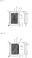
- Fig. 1 is a schematic cross-sectional view of an electron emission device of an embodiment according to the invention;
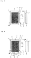
- Figs. 2 to 4 are schematic cross-sectional views each showing an electron emission device of another embodiment according to the invention;
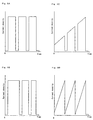
- Figs. 5A, 5B, 5C and 5D are graphs each illustrating a relationship between the current density and the processing period during the anodic oxidation treatment for fabricating an electron emission device of an embodiment according to the invention; and
- Fig. 6 is a graph illustrating relationships of both the diode current Ips and the emission current Iem with respect to the driving voltage Vps applied for driving the electron emission device together with that of a comparative electron emission device.
-
- Preferred embodiments according to the present invention will be described in more detail with reference to the accompanying drawings.
- As shown in Fig. 1, the electron emission device using a porous semiconductor layer embodying the present invention comprises a
porous semiconductor layer 13, a thin-film metal electrode 15 and a carbon region or thin film made of carbon or acarbon compound 40 which are formed in turn on asilicon layer 12 provided with anohmic electrode 11 at the back side. Theporous semiconductor layer 13 is formed by an anodic oxidation of theSi semiconductor layer 12 after the formation thereof. As for the whole, theporous semiconductor layer 13 has a thickness ranging of from 1 to 50 micrometers. As for the material of thecarbon region 40, forms of carbon such as amorphous carbon, graphite, carbyne, fullerene (C2n), diamond-like carbon, carbon nano-tube, and diamond etc., or carbon compounds such as ZrC, SiC, WC, and MoC etc. are effective. - As for the film formation method in manufacturing such electron emission devices, a physical or chemical method is used. The physical methods are known as physical vapor deposition (PVD) and include a vacuum deposition method, molecular beam epitaxy method, sputtering method, ionized vapor deposition method and laser abrasion method. The chemical methods are known as chemical vapor deposition (CVD) and include thermal CVD, plasma CVD and MOCVD (metal-organic chemical vapor deposition) etc. Among these methods, the sputtering method is especially effective.
- Furthermore, as shown in Fig. 2, the carbon regions may be provided as a thin-
film metal electrode 15a by having them distributed within the thin-film metal electrode. In this case, after the formation process for theporous semiconductor layer 13 through the anodic oxidation of thesemiconductor layer 12, the formation process of the carbon region is performed as the thin-film metal electrode formation process in which the thin-film metal electrode 15a containing the carbon region is formed over theporous semiconductor layer 13, with carbon or a carbon compound being mixed with the metal by using i.e. a mixed target or by sputtering within a carbon or carbon compound gas atmosphere. - Alternatively, the
carbon region 40 may be formed as a thin film deposited under the thin-film metal electrode 15 as shown in Fig. 3. In this case, the forming process of the carbon region is performed after the formation process of theporous semiconductor layer 13, followed by the formation process of the thin-film metal electrode 15 over thecarbon region 40. In this way, the formation process of the carbon region is performed immediately before the formation process of the thin-film metal electrode 15. The structure shown in Fig. 3 is obtained in which thecarbon region 40 is formed between the thin-film metal electrode 15 and theporous semiconductor layer 13. - The porous semiconductor electron emission device can be regarded as a diode of which the thin-
film metal electrode 15 at its surface is connected to a positive potential Vps and the back, i.e.,ohmic electrode 11 is connected to a ground potential. When the voltage Vps is applied between theohmic electrode 11 and the thin-film metal electrode 15 to supply electrons into thesemiconductor layer 12 of semiconductor Si, a diode current Ips flows. Since theporous semiconductor layer 13 has a high resistance, most of the applied electric field is applied to theporous semiconductor layer 13. The electrons travel inside theporous semiconductor layer 13 toward the thin-film metal electrode 15. Some of the electrons that reach near the thin-film metal electrode 15 pass through the thin-film metal electrode 15, due to the strong electric field, to be discharged out into a vacuum space 4 if the vacuum space exists in the outside. - In a case where the porous semiconductor electron emission device is used as a light-emitting device, the device substrate provided with the porous semiconductor electron emission devices is used as the first substrate at the backside, and a transparent
second substrate 1 such as one made of glass is retained as the front side substrate via a vacuum space 4 as shown in Fig. 1. On the internal surface of thesecond substrate 1, atransparent collector electrode 2 made of indium-tin oxide (what we call ITO), tin oxide (SnO) or zinc oxide (ZnO) etc. and a phosphor layer of R, G or B are formed in turn. To fabricate a color display device using the porous semiconductor electron emission devices, thecollector electrodes 2 capturing emitted electrons are grouped per three for R, G and B color signals corresponding to Red, Green and Blue emitting portions. Thus,fluorescent material layers corresponding collector electrodes 2. The electrons e (emission current Iem) discharged from thecarbon region 40 are accelerated by a high voltage Vc which is applied to the opposing collector electrode (transparent electrode) 2, and are collected at theelectrode 2. The fluorescent material layers coated on thecollector electrode 2 emit corresponding visible luminous energy. - Fig. 4 shows another embodiment of the present invention which is the same as the above embodiment comprising the
ohmic electrode 11, thesemiconductor layer 12 and the thin-film metal electrode 15, except that theporous semiconductor layer 13 consists of at least two or more of porosity-changedlayers - As shown in Fig. 4, the
porous semiconductor layer 13 is formed so that a porosity-changed layer with ahigh porosity 13a and a porosity-changed layer with alow porosity 13b may be alternately layered by in the thickness direction. The porosity-changed layer with ahigh porosity 13a thus has an electrical resistance lower than that of the porosity-changed layer with alow porosity 13b. - In addition, the high porosity-changed
layer 13a and/or low porosity-changedlayer 13b may be formed in such a manner that each may have an incline porosity gradually ascended in the thickness direction. Alternatively the incline porosity may be gradually descended in the thickness direction. - Thus, the change in porosity is given into the
porous semiconductor layer 13. The porosity-changed layer with alow porosity 13b having a high resistance should be flatly formed on the outer-most surface. The low porosity-changedlayer 13b prevents a superfluous current of the diode current Ips, and improves the contact with the thin-film metal electrode 15 formed thereon. Moreover, since the porosity-changed layer with alow porosity 13b is layered by turns, the thermal dissipation of the device will be promoted. - To repeatedly form the lamination combination of the high and low porosity-changed
layers layers - The electron emission device emits electrons although the thin-film electrode of metal such as Pt is simply prepared on the low porosity-changed
layer 13b. Alternatively, after anodization for making pores on the semiconductor layer, oxidization or nitriding may be performed on the resulted porous semiconductor layer under the following conditions and, after that, the thin-film electrode of metal such as Pt is prepared, so that an emission stability and durability of the device are improved more. - The porous semiconductor layer may be oxidized under the oxidization conditions of a temperature ranging from 700 to 1200 degrees Centigrade and a time period of
form 1 to 120 minutes in oxygen gas, alternatively under the oxidization conditions of a temperature ranging from 200 to 900 degrees Centigrade and a time period ofform 1 to 120 minutes in oxygen plasma. The porous semiconductor layer may be nitrided under the nitriding conditions of a temperature ranging from 700 to 1200 degrees Centigrade and a time period ofform 1 to 120 minutes in nitrogen gas, alternatively under the nitriding conditions of a temperature ranging from 200 to 900 degrees Centigrade and a time period ofform 1 to 120 minutes in nitrogen plasma. - In addition, a Si wafer of a single-crystalline, amorphous, poly-crystalline, n-type or p-type may be used for a device-substrate in which the porous Si layer is formed through the anodization. Alternatively, the thin Si layer may be deposited on the ohmic electrodes previously formed on a substrate. This case is convenient to a display device comprising a plurality of electron emission devices.
- Although sputtering is particularly effective in forming those layers and the substrate, vacuum deposition method, CVD (Chemical Vapor Deposition), laser ablation method, MBE (Molecular Beam Epitaxy) and ion beam sputtering are also effective.
- The material of the
semiconductor layer 12 preferably used is silicon (Si), but not restricted in the present invention. In addition to the semiconductor layer of silicon, there may be used for thesemiconductor layer 12 semiconductor materials capable of being treated by means of an anodic treatment method, for example, a single substance or compound semiconductor of Group IV, Group III-V or Group II-VI such as germanium (Ge), silicon carbide (SiC), gallium arsenide (GaAs), phosphoric indium (InP), cadmium selenide (CdSe). When employing the crystalline for theSi layer 12, the crystal substrate having its surface (100) direction orientating perpendicular to its major surface is preferably used, because the electron emission efficiency η of the porous Si layer is better. It is estimated that such a (100) Si layer provides the Si crystalline direction and minute pore channels with a nano-order diameter which orientate perpendicular to its major surface. In addition, the employment of the porous Si layer made from the amorphous Si layer provides amorphous residual Si skeletons and minute channels. - The
porous semiconductor layer 13 is formed in thesemiconductor wafer 12 through the anodic treatment. For example. asemiconductor wafer 12 of an n-type Si is preformed by an anodic treatment, in which an insulative layer with a rectangle opening is previously formed on the semiconductor wafer. The semiconductor wafer is then dipped into a hydrogen fluoride (HF) solution bath. The surface of the semiconductor layer is partially exposed in the HF solution through the opening of the insulative layer. The exposed semiconductor layer as an anode and the cathode of Pt are disposed facing to each other in the HF solution. The anode and cathode are connected to a DC power supply, so that a DC current is applied across these electrodes with a low current density to anodize the exposed semiconductor layer. As a result, a p-type porous Si layer is formed in the Si substrate. In this embodiment, the formation of the porous structure requires the consumption of positive holes and thus the light-irradiation should be preformed during the anodization to supply the positive hole carriers to the exposed semiconductor layer. Alternatively, the porous Si layer may be formed on a p-type Si semiconductor layer. In this case, the porous Si layer may be formed even if it is in a dark condition. - The porous Si layer is consisted of plural minute channels or open spaces and the residual Si . When the pore channel's diameter is in a range from approximately one to several hundreds nano-meters and the dimension of each residual Si skeleton is in a range from the number of tens to hundreds of Si atoms, it is expected that an electron emission phenomenon occurs due to the quantum size effect. These values may be controlled by the settings of the conditions of the HF density, the current density, the duration of anodization treatment and the light-irradiation time period during the anodic treatment.
- By controlling the current density and the processing period in the anodizing treatment of the semiconductor layer, the porosity is changed at 10 to 80% in the thickness direction of the
porous semiconductor layer 13 having the porosity-changedlayers layers layer 13b), but such internal diameter of the pore channel increases as its depth becomes deeper (i.e., the porosity-changedlayer 13a). In this case, the long processing periods with a high current density are equal to each other for forming the porosity-changed layers with ahigh porosity 13a intermittently, as shown in Fig. 5A. The long processing periods with a high current density may be gradually made short for forming the high porosity-changedlayers 13a becoming thin gradually, as shown in Fig. 5B. - Moreover, at least two or more of the porosity-changed layers each having a porosity different from the contiguities in the thickness direction can also be formed in the porous semiconductor layer by means of anodizations under the conditions of the current densities and the processing periods as shown in Figs. 6C and 6D. By controlling the current densities and processing periods, the specific resistance becomes small so that it is close to the
Si layer 12 in each layer. There are a gradual slope of porosity proportional to the resistivity in each porosity-changedlayer 13a formed by the anodization as shown in Fig. 5C or 5D. For porosity slope of the thickness direction in the porous silicon layer, the current density is gradually changed during the anodization. Theporous Si layer 13 may have a high resistivity at a portion adjacent to its surface and a low resistivity at a portion adjacent to its interface between theporous Si layer 13 and theSi substrate 12. This continuous incline of resistivity in theporous Si layer 13 is preferable for the injection of electrons from the substrate. - Although metals such as Pt, Au, W, Ru and Ir are effective as the material for the thin-
film metal electrode 15 on the electron emission side, Al, Sc, Ti, V, Cr, Mn, Fe, Co, Ni, Cu, Zn, Ga, Y, Zr, Nb, Mo, Tc, Rh, Pd, Ag, Cd, Ln, Sn, Ta, Re, Os, Tl, Pb, La, Ce, Pr, Nd, Pm, Sm, Eu, Gd, Tb, Dy, Ho, Er, Tm, Yb, Lu and an alloy of individuals thereof can be used as well. From the principle of electron emission, it is better that the material for the thin-film metal electrode 15 has a lower work function and is thinner. To increase the electron emission efficiency, the material for the thin-film metal electrode 15 should be a metal of the group I or group II in the periodic table; for example, Cs, Rb, Li, Sr, Mg, Ba, Ca and the like are effective and alloys of those elements may be used as well. To make the thin-film metal electrode 15 very thin, the material for the thin-film metal electrode 15 should be a chemically stable metal with a high conductivity; for example, single substances of Au, Pt, Lu, Ag and Cu or alloys thereof are desirable. It is effective to coat or dope a metal with a low work function as described above on or in those metals. Utilizable efficiency is obtained by using an Au or Pt thin-film electrode having a thickness of from 1 to 50 nm. When considering the stability as an electron emission device, a thickness of from 2 to 20 nm is the most suitable for the Au or Pt thin-film electrode. - The material for the
ohmic electrodes 11 is Au, Pt, Al, W or the like which is generally used for the wires of an IC, and has a uniform thickness for supplying substantially the same current to the individual devices. - The material for another device-substrate (not shown) on which the
semiconductor Si layer 12 is deposited as a thin-film may be ceramics such as Al2O3, Si3N4 or BN instead of glass. - Concretely, the electron emission devices were produced from Si wafers of 14mm x 14mm, and their characteristic were investigated.
- While the current density and the processing period of anodization were changed in the anodization method using the Si wafer, the processing of the short time for which current density was reduced was performed intermittently. As a result, the thin porosity-changed layers were formed in the porous semiconductor layer of the Si wafer, in each of which the average pore diameter was 1/20 and the average number of pores was 400 times per centimeter square in comparison with that of the conventional device. The anodization conditions were as follows:
-
- Ingredients of the electrolytic solution (temperature):
- HF : Ethanol = 1 : 1 (at 0 degree Centigrade)
- Current density and processing period:
- A set of (2.5mA/cm2 for 2 seconds and 50mA/cm2 for 10 seconds) times 3 equals a total of 36 seconds.
- Thickness of the porous semiconductor layer:
- A set of (porosity-changed layers of 0.016µm and 1.67 µm thick) times 3 equals a total of 5.058µm thick.
-
- The same electron emission device was produced as comparative examples in such a manner as the above-mentioned case except having a conventional porous silicon layer with a uniform porosity. At this case, it carried out under the following anodization conditions.
-
- Ingredients of the electrolytic solution (temperature):
- HF : Ethanol = 1 : 1 (at 0 degree Centigrade)
- Current density and processing period:
- It is 50mA/cm2 constant for a whole period. processing period: 30 seconds
- Thickness of the porous semiconductor layer: 5µm
- An ohmic electrode was formed at the back side of each Si wafer after anodized.
-
- Finally, a 6 mm diameter thin-film metal electrode of Pt was formed 6 nm thick on the surface of the amorphous SiO2 layer of each substrate by sputtering, thus providing a plurality of device-substrates.
- Meanwhile, transparent substrates were prepared, each of which has a collector electrode of indium tin oxide (ITO) formed inside a transparent glass substrate and has a fluorescent layer of a fluorescent substance corresponding to R, G or B color emission formed on the collector electrode by the normal scheme.
- Electron emission devices were assembled in each of which the device-substrate and the transparent substrate are supported apart from one another by 10 mm in parallel by a spacer in such a way that the thin-
film metal electrode 15 faced thecollector electrode 2, with the clearance therebetween made to a vacuum of 10-5 Pa. - Then, the diode current Ips and the emission current Iem corresponding to the thickness of the SiO2 film of each of the acquired plural devices were measured.
- This result is shown in Fig. 6. As for the device of the invention, as seen from the figure, only the diode current Ips was restricted, without carrying out an emission current Iem fall, and electron emission efficiency η improved from 10-3 to 10-1 no less than 2 figures in comparison with that of the conventional device.
- Moreover, fluctuations of temperature of the electron emission devices both of the embodiment and the comparative example were measured when the same voltage Vps was applied to each device. The electron emission device of the invention generally exhibited a uniform declining of temperature upon application of the constant voltage Vps, in comparison with that of the comparative example.
- When a voltage of approximately 4 kV applied across the fluorescent-substance coated collector electrode and the thin-film metal electrode, a uniform fluorescent pattern corresponding to the shape of the thin-film metal electrode was observed in the devices. This shows that the uniform electron emission is caused by the porous semiconductor layer having at least two or more of porosity-changed layers which have porosities which are different from each other in the thickness direction and the emission exhibits a high linearity, and that those devices can serve as an electron emission diode, or a light-emitting diode or laser diode which emits electromagnetic waves of infrared rays, visible light or ultraviolet rays.
- As mentioned above, according to the present invention, the electron emission device comprising the carbon region made of carbon or a carbon compound provided on top or under, or inside of the thin-film metal electrode, prevents a superfluous flow of diode current Ips during the operation of device to provide a high electron emission efficiency η (η = emission current Iem/diode current Ips). In addition, the present invention eliminates the problem of the contact between the porous semiconductor layer and the thin-film metal electrode formed thereon to make the electron emission stable. Such a contact problem is caused by a phenomenon that the rough surface of the porous semiconductor layer after the anodic oxidation prevents from contacting closely with the thin-film metal electrode.
Claims (11)
- An electron emission device comprising:a semiconductor layer for supplying electrons;a porous semiconductor layer formed on the semiconductor layer; anda thin-film metal electrode which is formed on the porous semiconductor layer and faces a vacuum space, further comprising a carbon region made of carbon or a carbon compound provided on top or under, or inside of said thin-film metal electrode, whereby the electron emission device emits electrons when an electric field is applied between the semiconductor layer and the thin-film metal electrode.
- An electron emission device according to claim 1, wherein said thin-film metal electrode and said carbon region are deposited through a physical deposition method or a chemical deposition method.
- An electron emission device according to claim 1, wherein said carbon region is a thin film deposited on said thin-film metal electrode.
- An electron emission device according to claim 1, wherein said carbon region is distributed within said thin-film metal electrode.
- An electron emission device according to claim 1, wherein said carbon region is a thin film deposited under said thin-film metal electrode.
- An electron emission device according to claim 1, wherein the porous semiconductor layer is formed by an anodization processing to the surface of the semiconductor layer to be made as a porous portion.
- An electron emission device according to claim 6, wherein the porous semiconductor layer has at least two or more of porosity-changed layers which have porosities which are different from each other in the thickness direction.
- An electron emission device according to claim 7, wherein the porosity-changed layer with a high porosity and another porosity-changed layer with a low porosity are layered by turns in the thickness direction of the porous semiconductor layer.
- An electron emission device according to claim 8, wherein the semiconductor layer is anodic-oxidized from the surface thereof in such a manner that a first processing time duration in which a low current density for the anodization processing is applied to the surface and a second processing time duration in which a high current density for the anodization processing is applied to the surface are repeated by turns, so that the porosity-changed layer with a high porosity and another porosity-changed layer with a low porosity are layered by turns in the thickness direction of the porous semiconductor layer.
- An electron emission device according to claim 7, wherein the porosity-changed layers have incline porosities ascended or descended gradually in the thickness direction.
- An electron emission device according to claim 10, wherein the semiconductor layer is anodic-oxidized from the surface thereof during a processing time in which a current density for the anodization processing is changed so that the porosity-changed layers have incline porosities in the thickness direction.
Applications Claiming Priority (2)
| Application Number | Priority Date | Filing Date | Title |
|---|---|---|---|
| JP30507199 | 1999-10-27 | ||
| JP30507199A JP3789064B2 (en) | 1999-10-27 | 1999-10-27 | Electron emitter |
Publications (2)
| Publication Number | Publication Date |
|---|---|
| EP1096532A1 true EP1096532A1 (en) | 2001-05-02 |
| EP1096532B1 EP1096532B1 (en) | 2005-12-28 |
Family
ID=17940774
Family Applications (1)
| Application Number | Title | Priority Date | Filing Date |
|---|---|---|---|
| EP20000123265 Expired - Lifetime EP1096532B1 (en) | 1999-10-27 | 2000-10-26 | Electron emission device |
Country Status (3)
| Country | Link |
|---|---|
| EP (1) | EP1096532B1 (en) |
| JP (1) | JP3789064B2 (en) |
| DE (1) | DE60025134T2 (en) |
Cited By (6)
| Publication number | Priority date | Publication date | Assignee | Title |
|---|---|---|---|---|
| EP1255272A3 (en) * | 2001-04-30 | 2003-08-13 | Hewlett-Packard Company | Silicon electron emitter |
| WO2003077320A1 (en) * | 2002-03-08 | 2003-09-18 | Matsushita Electric Works, Ltd. | Quantum device |
| EP1328003A3 (en) * | 2001-12-13 | 2004-03-17 | Matsushita Electric Works, Ltd. | Field emission-type electron source |
| US6720717B2 (en) | 2001-09-25 | 2004-04-13 | Matsushita Electric Works, Ltd. | Field emission-type electron source |
| EP1523025A3 (en) * | 2002-03-25 | 2005-04-20 | Matsushita Electric Works, Ltd. | Field emission-type electron source |
| DE102020113351B4 (en) * | 2020-05-18 | 2026-03-19 | Dbt Gmbh | Semiconductor-based direct emitter, and liquid ionizer with the same, method for generating free electrons |
Families Citing this family (1)
| Publication number | Priority date | Publication date | Assignee | Title |
|---|---|---|---|---|
| WO2006126383A1 (en) * | 2005-05-24 | 2006-11-30 | Konica Minolta Holdings, Inc. | Field emission electron source and method for manufacturing same |
Citations (4)
| Publication number | Priority date | Publication date | Assignee | Title |
|---|---|---|---|---|
| US5430300A (en) * | 1991-07-18 | 1995-07-04 | The Texas A&M University System | Oxidized porous silicon field emission devices |
| EP0874384A1 (en) * | 1997-03-25 | 1998-10-28 | Pioneer Electronic Corporation | Electron emission device and display device using the same |
| EP0913849A2 (en) * | 1997-10-29 | 1999-05-06 | Matsushita Electric Works, Ltd. | Field emission electron source, method of producing the same, and use of the same |
| JPH11265653A (en) * | 1998-03-18 | 1999-09-28 | Ulvac Corp | Electrode, and display device having the electrode |
-
1999
- 1999-10-27 JP JP30507199A patent/JP3789064B2/en not_active Expired - Fee Related
-
2000
- 2000-10-26 EP EP20000123265 patent/EP1096532B1/en not_active Expired - Lifetime
- 2000-10-26 DE DE2000625134 patent/DE60025134T2/en not_active Expired - Fee Related
Patent Citations (4)
| Publication number | Priority date | Publication date | Assignee | Title |
|---|---|---|---|---|
| US5430300A (en) * | 1991-07-18 | 1995-07-04 | The Texas A&M University System | Oxidized porous silicon field emission devices |
| EP0874384A1 (en) * | 1997-03-25 | 1998-10-28 | Pioneer Electronic Corporation | Electron emission device and display device using the same |
| EP0913849A2 (en) * | 1997-10-29 | 1999-05-06 | Matsushita Electric Works, Ltd. | Field emission electron source, method of producing the same, and use of the same |
| JPH11265653A (en) * | 1998-03-18 | 1999-09-28 | Ulvac Corp | Electrode, and display device having the electrode |
Non-Patent Citations (1)
| Title |
|---|
| PATENT ABSTRACTS OF JAPAN vol. 1999, no. 14 22 December 1999 (1999-12-22) * |
Cited By (8)
| Publication number | Priority date | Publication date | Assignee | Title |
|---|---|---|---|---|
| EP1255272A3 (en) * | 2001-04-30 | 2003-08-13 | Hewlett-Packard Company | Silicon electron emitter |
| US6720717B2 (en) | 2001-09-25 | 2004-04-13 | Matsushita Electric Works, Ltd. | Field emission-type electron source |
| EP1328003A3 (en) * | 2001-12-13 | 2004-03-17 | Matsushita Electric Works, Ltd. | Field emission-type electron source |
| WO2003077320A1 (en) * | 2002-03-08 | 2003-09-18 | Matsushita Electric Works, Ltd. | Quantum device |
| US6940087B2 (en) | 2002-03-08 | 2005-09-06 | Matsushita Electric Works, Ltd. | Quantum device |
| EP1484800A4 (en) * | 2002-03-08 | 2008-10-29 | Matsushita Electric Works Ltd | QUANTUM DEVICE |
| EP1523025A3 (en) * | 2002-03-25 | 2005-04-20 | Matsushita Electric Works, Ltd. | Field emission-type electron source |
| DE102020113351B4 (en) * | 2020-05-18 | 2026-03-19 | Dbt Gmbh | Semiconductor-based direct emitter, and liquid ionizer with the same, method for generating free electrons |
Also Published As
| Publication number | Publication date |
|---|---|
| JP2001126610A (en) | 2001-05-11 |
| EP1096532B1 (en) | 2005-12-28 |
| DE60025134D1 (en) | 2006-02-02 |
| DE60025134T2 (en) | 2006-07-20 |
| JP3789064B2 (en) | 2006-06-21 |
Similar Documents
| Publication | Publication Date | Title |
|---|---|---|
| EP0798761B1 (en) | Cold electron emission display device | |
| EP0874384B1 (en) | Electron emission device | |
| US20030197457A1 (en) | Field emission electron source | |
| US6940087B2 (en) | Quantum device | |
| WO1997049119A1 (en) | Photoelectronic material, device using the same, and method for manufacturing the same | |
| WO2003049132A1 (en) | Electron emitting device and method of manufacturing the same and display apparatus using the same | |
| KR100374782B1 (en) | Field emision-type electron source and manufacturing method thereof | |
| US6017773A (en) | Stabilizing process for porous silicon and resulting light emitting device | |
| EP1096532B1 (en) | Electron emission device | |
| US5986390A (en) | Electron emission device having peak intensity ratio characteristic of raman spectrum for fold ring of SiO2 | |
| JPH11186607A (en) | Compound semiconductor light emitting device | |
| JP3537624B2 (en) | Electron-emitting device | |
| JP2000164921A (en) | Semiconductor light emitting material, method of manufacturing the same, and light emitting device using the same | |
| US6771010B2 (en) | Silicon emitter with low porosity heavily doped contact layer | |
| KR100593543B1 (en) | Nitride semiconductor light emitting device and its manufacturing method | |
| JP3249189B2 (en) | Group IV semiconductor device containing carbon | |
| JPWO2000074098A1 (en) | Thin-film electron source, display device using same, and application equipment | |
| JPH0690018A (en) | Light emitting device and manufacturing method thereof | |
| JP3323871B2 (en) | Method for manufacturing semiconductor device | |
| JP3544296B2 (en) | Electron-emitting device | |
| JP4040135B2 (en) | Manufacturing method of ZnSe-based compound semiconductor laser | |
| JP3335161B2 (en) | Field emission electron source | |
| JP4658643B2 (en) | Boron phosphide semiconductor device | |
| JPS59119776A (en) | Light emitting semiconductor device | |
| KR20070031831A (en) | Field emitter device |
Legal Events
| Date | Code | Title | Description |
|---|---|---|---|
| PUAI | Public reference made under article 153(3) epc to a published international application that has entered the european phase |
Free format text: ORIGINAL CODE: 0009012 |
|
| AK | Designated contracting states |
Kind code of ref document: A1 Designated state(s): DE FR GB |
|
| AX | Request for extension of the european patent |
Free format text: AL;LT;LV;MK;RO;SI |
|
| 17P | Request for examination filed |
Effective date: 20010712 |
|
| AKX | Designation fees paid |
Free format text: DE FR GB |
|
| GRAP | Despatch of communication of intention to grant a patent |
Free format text: ORIGINAL CODE: EPIDOSNIGR1 |
|
| GRAS | Grant fee paid |
Free format text: ORIGINAL CODE: EPIDOSNIGR3 |
|
| GRAA | (expected) grant |
Free format text: ORIGINAL CODE: 0009210 |
|
| AK | Designated contracting states |
Kind code of ref document: B1 Designated state(s): DE FR GB |
|
| REG | Reference to a national code |
Ref country code: GB Ref legal event code: FG4D |
|
| REF | Corresponds to: |
Ref document number: 60025134 Country of ref document: DE Date of ref document: 20060202 Kind code of ref document: P |
|
| ET | Fr: translation filed | ||
| REG | Reference to a national code |
Ref country code: GB Ref legal event code: 746 Effective date: 20060925 |
|
| PLBE | No opposition filed within time limit |
Free format text: ORIGINAL CODE: 0009261 |
|
| STAA | Information on the status of an ep patent application or granted ep patent |
Free format text: STATUS: NO OPPOSITION FILED WITHIN TIME LIMIT |
|
| 26N | No opposition filed |
Effective date: 20060929 |
|
| PGFP | Annual fee paid to national office [announced via postgrant information from national office to epo] |
Ref country code: FR Payment date: 20071019 Year of fee payment: 8 Ref country code: GB Payment date: 20071022 Year of fee payment: 8 |
|
| PGFP | Annual fee paid to national office [announced via postgrant information from national office to epo] |
Ref country code: DE Payment date: 20071228 Year of fee payment: 8 |
|
| GBPC | Gb: european patent ceased through non-payment of renewal fee |
Effective date: 20081026 |
|
| REG | Reference to a national code |
Ref country code: FR Ref legal event code: ST Effective date: 20090630 |
|
| PG25 | Lapsed in a contracting state [announced via postgrant information from national office to epo] |
Ref country code: DE Free format text: LAPSE BECAUSE OF NON-PAYMENT OF DUE FEES Effective date: 20090501 |
|
| PG25 | Lapsed in a contracting state [announced via postgrant information from national office to epo] |
Ref country code: FR Free format text: LAPSE BECAUSE OF NON-PAYMENT OF DUE FEES Effective date: 20081031 |
|
| PG25 | Lapsed in a contracting state [announced via postgrant information from national office to epo] |
Ref country code: GB Free format text: LAPSE BECAUSE OF NON-PAYMENT OF DUE FEES Effective date: 20081026 |