EP1096295A1 - Dispositif et procédé pour améliorer la résolution de capteurs optiques - Google Patents
Dispositif et procédé pour améliorer la résolution de capteurs optiques Download PDFInfo
- Publication number
- EP1096295A1 EP1096295A1 EP99121512A EP99121512A EP1096295A1 EP 1096295 A1 EP1096295 A1 EP 1096295A1 EP 99121512 A EP99121512 A EP 99121512A EP 99121512 A EP99121512 A EP 99121512A EP 1096295 A1 EP1096295 A1 EP 1096295A1
- Authority
- EP
- European Patent Office
- Prior art keywords
- sensor according
- optical system
- matrix
- linear
- technique
- Prior art date
- Legal status (The legal status is an assumption and is not a legal conclusion. Google has not performed a legal analysis and makes no representation as to the accuracy of the status listed.)
- Ceased
Links
Images

Classifications
-
- G—PHYSICS
- G02—OPTICS
- G02B—OPTICAL ELEMENTS, SYSTEMS OR APPARATUS
- G02B27/00—Optical systems or apparatus not provided for by any of the groups G02B1/00 - G02B26/00, G02B30/00
- G02B27/42—Diffraction optics, i.e. systems including a diffractive element being designed for providing a diffractive effect
- G02B27/46—Systems using spatial filters
-
- G—PHYSICS
- G02—OPTICS
- G02B—OPTICAL ELEMENTS, SYSTEMS OR APPARATUS
- G02B27/00—Optical systems or apparatus not provided for by any of the groups G02B1/00 - G02B26/00, G02B30/00
- G02B27/58—Optics for apodization or superresolution; Optical synthetic aperture systems
Definitions
- the present invention relates generally to optical devices, and more particularly to an optical sensor which is specifically configured to be utilized in conjunction with an image processing technique in order to provide a much higher level of resolution without significantly increasing the size of the sensor.
- Optical sensors are devices which for decades have been utilized to detect and record various optical images.
- Various types of optical sensors have been developed which work in the Ultra Violet Bands, Infra Red Bands as well as in the Visible Bands of operation. Examples of such devices include Weather Sensors, Terrain Mapping Sensors, Surveillance Sensors, Medical Probes, Telescopes and Television Cameras.
- An optical sensor typically includes an optical system and one or more detectors.
- the optical system portion is made up of various combinations of lenses, mirrors and filters which is utilized to focus light onto a focal plane located at the image plane of the optical system.
- the detectors which make up the image plane is utilized to convert the light received from the optical system into electrical signals.
- other types of optical sensors utilize film to record the images. In this case, the grain size of the film is analogous to the detectors described above.
- spatial resolution is the size of the smallest object that can be resolved in the image, or equivalently is the ability to differentiate between closely spaced objects. If the optical system of these sensors are free from optical aberrations which means being “well corrected” the spatial resolution is ultimately limited by one of two factors. Either the resolution is limited by the size of the detectors in the focal plane or by diffraction effects.
- Diffraction is a well known characteristic of light which among other things describes how light passes through an aperture of an optical system. Diffraction causes the light passing through an aperture to spread out which causes points of an image not to be a point, but rather a pattern of light known as a diffraction pattern diffused across a focal plane.
- the diffraction pattern includes a very bright central spot, surrounded by bright and dark rings of much less intensity which decrease in intensity as the distance from the ring to the central spot increases.
- An optical sensor that is designed to be diffraction limited, typically, has a very well corrected optical system and detectors sized so that the central spot of the diffraction pattern just fits within the active area of the detector. Making the detectors any smaller does not serve any purpose and is considerably more costly due to the added cost of the extra detectors and the associated electronics.
- the size of the aperture utilized in the optical system also is an important factor due to diffraction effects.
- the size of the aperture is expressed differently depending on the type of application.
- the aperture In applications such as camera lenses and telescope objectives, the aperture is normally expressed as a f-number which is the ratio of the effective focal length to the size of the clear aperture.
- the aperture In applications such as microscope objectives, the aperture is normally expressed as a Numerical aperture (NA) which is the index of refraction times the sine of the half angle of the cone of illumination. For a given focal length, a high f-number corresponds to a smaller aperture, while a higher Numerical aperture corresponds to a larger aperture.
- NA Numerical aperture
- a drawback with conventional optical sensors relates to the size of the aperture required for a given level of resolution.
- a larger aperture is required.
- the use of such a system is very costly. This is because utilizing a larger 25 aperture requires the use of a significantly larger optical system.
- the cost for larger systems which have apertures with diameters greater than one foot is proportional to the diameter of the aperture raised to a power of "x".
- the variable "x" typically ranges from 2.1 to 2.9 depending on a number of other particulars associated with the sensor such as its wave band, field of regard and field of view.
- the consideration for the size of the optical sensor is particularly relevant in systems that fly on some type of platform, either in space or in the air. Under such conditions, the sensor must be light weight, strong and capable of surviving the rigors of the flight environment. Thus, the cost of going to a larger optical system can be in the hundreds of millions of dollars for some of the larger and more sophisticated sensors. Further, the size of the sensor may also be limited by such practical considerations as the amount of weight or space the host rocket, plane, balloon or vehicle accommodates. In these situations, a larger system cannot be implemented regardless of the cost.
- a number of optical imaging techniques have been developed which are directed at increasing spatial resolution.
- One such example attempts to increase the resolution of optical sensors by utilizing a condition known as sub-pixel resolution.
- sub-pixel resolution the optical system is limited in spatial resolution not by diffraction, but by the size of the detectors or pixels. In this case, a larger detector size is utilized to prevent a portion of the higher spatial frequencies of the image formed by the optical system from being observed.
- sub-pixel resolution attempts to reconstruct an image that includes these higher spatial frequencies which are already in the image.
- This technique does not attempt to reconstruct an image that is smaller than the diffraction limit, which is even smaller than the sub-pixel resolution. Further, this technique also does not require hardware or system operation changes in order to achieve sub-pixel reconstruction.
- optical imaging techniques are disclosed in another article entitled SUPERRESOLUTION ALGORITHMS FOR A MODIFIED HOPFIELD NEURAL NETWORK, by J.B. Abbiss, IEEE Transactions On Signal Processing, Vol. 39, No. 7, July 1991 and in a paper entitled FAST REGULATED DECONVOLUTION IN OPTICS AND RADARS, by J.B. Abbiss, presented at the 3rd IMA Conference on Mathematics in Signal Processing. These techniques utilize linear equation and matrix techniques in order to restore signals or images from a limited discrete data set.
- an object of the present invention to provide a technique for increasing the resolution of an optical sensor without utilizing a substantially larger aperture.
- An optical sensor is disclosed of the type typically including an optical system for focusing light onto a focal plane.
- the optical system having a predetermined Numerical aperture which provides a corresponding level of spatial resolution.
- the optical sensor also including means for converting the light focused onto the focal plane into electrical signals including imaging data.
- the optical sensor further including means for processing the imaging data in order to provide a desired level of spatial resolution which is substantially higher than the corresponding level of spatial resolution.
- the present invention is directed to an optical sensor which overcomes the difficulty of requiring larger apertures in order to achieve resolutions below the diffraction limit.
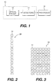
- the sensor 10 as in conventional devices includes an optical system 12 and detectors 14.
- the optical system 12 which includes various combinations of lenses, mirrors and filters depending on the type of application is utilized to focus light onto a focal plane where the detectors 14 are located.
- the optical system 12 also includes a predetermined aperture size corresponding to a particular Numeral aperture (NA) which in conventional diffraction limited devices limits the amount of spatial resolution that is attainable. As previously described, this is due to diffraction blurring effects.
- NA Numeral aperture
- the detectors 14 are utilized to convert the light received from the optical system 12 into electrical signals which includes the imaging data utilized to generate images.
- the detectors are configured in a linear array for Scanning systems or in a matrix array for Starring systems.
- Scanning systems the detector linear array is swept in a direction perpendicular to the length of the array which generates imaging data one scan line at a time which corresponds to one line of the image.
- Starring systems the matrix array is not moved and generates all of the imaging data for the image simultaneously.
- each detector of the matrix array corresponds to one pixel of the image. It is intended that the detectors 14 of the present invention are also configurable as a linear array or a matrix array depending on the type of system being utilized.
- the detectors 14 are also capable of being embodied by a number of different type of devices depending on the wavelength of light utilized by the present invention.
- such detectors in the ultraviolet and X-Ray range such detectors as semitransparent photocathodes and opaque photocathodes are capable of being utilized.
- such detectors include vacuum phototubes, photomultipliers, photoconductors and photodiodes, while in the infrared range, such detectors also include photoconductors, photodiodes, pryoelectric, photon drag and golay cells devices.
- the configuration of various elements of the sensor 10 is dependent on the particular image processing technique utilized. As will be described in detail later, the present invention includes at least five alternative image processing techniques.
- the senor 10 must include detectors 14 that have an "instantaneous field of view" that is equal or less than the desired level of spatial resolution.
- the required resolution is one meter or less
- the "instantaneous field of view" of the detectors must correspond to one meter or less, even though the central lobe of the diffraction pattern is much larger. This makes, the pixel size of the image produced by the sensor 10 smaller than the central diffraction lobe.
- Such a configuration adds additional cost to the sensors. However, for large systems the increase in cost is less than the cost of a larger system.
- the sensor 10 can be configured according to Case one in one of two ways.
- One way is to utilize a larger amount of detectors 14 and a smaller size of detectors 14.
- the number of detectors utilized varies any where from one to thousands or to millions depending on the type of application.
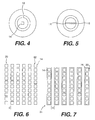
- FIG. 2 A diagram of a linear detector array according to the present invention is shown in FIGURE 2, while a diagram of a matrix detector array according to the present invention is shown in FIGURE 3.
- the number of detectors 14 included in these arrays 28,30 depends on the particular application. However, in order to achieve the higher resolution, these arrays will include a multiple of the number of detectors present in conventional sensors for a given application.
- the size of the individual detector is never smaller than size of the central diffraction lobe. This is because utilizing smaller sensors serves no purpose due to the resolution being limited by the optical aperture.
- the size of any individual detector 14 is smaller than the size of the central diffraction lobe 18, as illustratively depicted in FIGURE 4, and as shown in FIGURE 5 in connection with multiple detectors.
- the number of detectors within the central spot will vary depending on the particular application, but will be at least three detectors, preferably at least five detectors, and for instance may comprise six to nine detectors in some examples. In general, fewer detectors, (even as low as three or four) may be advantageous in high noise environments.
- Another way of configuring the sensor 10 according to Case one is to again utilize a larger number of detectors, but instead of utilizing smaller detectors, adjust the optical system 12 so that more than one detector is spread across the central diffraction lobe.
- This enables conventional size detectors 14 to be utilized.
- the number of detectors utilized is the same as previously discussed.
- the back focal length of the optical system 12 is adjusted, which is a well known procedure. Multiple detectors spread across the central diffraction lobe in accordance with this embodiment are also depicted in FIGURE 5.
- the senor 10 is configured to take multiple images of objects in a known pattern that moves each image by a known amount. This is accomplished by the sensor 10 viewing the object at different angles, wherein each image of the object corresponds to a different angle. The viewing at different angles is accomplished by the movement of the sensor 10 induced by jitter in the spacecraft or vehicle. This also is accomplished by jitter induced by a mirror included in the optical system 12.
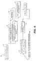
- the multi-linear array 20 includes a number of individual linear arrays 22 arranged in a parallel configuration staggered apart by a distance (d) which is a fraction of a pixel.
- d distance which is a fraction of a pixel.
- each linear array 22 generates imaging data corresponding to one scan line of each of the images.
- each linear array 22 corresponds to one of the images being produced.
- the array 20 includes ten or more individual linear arrays 22 which are capable of producing ten or more different images.
- the senor 10 is configured to take images of objects in multiple color bands. In Scanning systems, this is again accomplished by utilizing a multi-linear array, as shown in FIGURE 7.
- the multi-linear array 24 also includes a number of individual linear arrays 22 arranged in a parallel configuration staggered apart by a distance (d) which is a fraction of a pixel.
- a color filter 26 is disposed over each of the linear arrays 22.
- the color filters 26 are configured to pass only a particular portion of the color spectrum which may include one or more different wavelengths of visible light.
- each linear array 22 produces images of the same object in different color bands.
- the filters 26 are fabricated by disposing layers of optical coatings on transparent substrates, which are then placed over each of the linear arrays 22, which is a well known process.
- the multiple color band imaging data is accomplished by incorporating a beam splitter in the optical system 12 and utilizing more than one detector matrix array.
- a beam splitter in the optical system 12 and utilizing more than one detector matrix array.
- the beam splitter 28 is utilized to split the incoming light 32 into multiple light beams 34 which in this case is two. Due to the operation of the beam splitter 28 each of the light beams 34 includes a different portion of the color spectrum which may include one or more different wavelengths of visible or infrared light. Each light beam is then directed to one of the detector arrays 30 which produces the images of the same object in different color bands.
- the senor 10 is configured to have a combination of the three previously described cases. This is accomplished by combining the principles discussed in regard to case one, two or three. In regard to all of the cases previously described, the sensor must be configured to have a signal to noise ratio which is high as possible. This is accomplished by either increasing the integration time of the detectors 14 or by slowing down the scan speed as much as possible for scanning systems. For case two, the system's design or its operation mode, or both are changed in order to take the required multiple images in a known pattern displaced by a known distance that is not a multiple of a pixel, but rather is a multiple of a pixel plus a known fraction of a pixel.
- a processor 16 which is utilized to process the imaging data in order to attain the higher resolution.
- the processing includes recovering "lost” information from the imaging data which is utilized to provide the higher resolution. Even though the diffraction blur destroys the required spatial resolution, some of the "lost” spatial information still exists spread across the focal plane. Oversampling the diffraction blur in conjunction with processing the data correctly, enables much of this "lost” information to be recovered and thus enables the image to be restored to a higher spatial resolution than classical diffraction would allow.
- the processor 16 accomplishes the above described processing by utilizing one of five alternative image processing techniques including a Linear Algebra Technique, Multiple Image Reconstruction Technique, Non-linear Reconstruction Technique, Non-linear Multiple and Reconstruction Technique and various combinations of the above four techniques. Which of the above techniques is utilized by the processor 16, determines how the sensor 10 according to the present invention is configured.
- the sensor 10 For the Linear Algebra Technique, Non-linear Reconstruction Technique and Non-linear Multiple Band Reconstruction Technique, the sensor 10 must be configured according to Case one. For the Non-linear Multiple Band Reconstruction Technique, the sensor 10 must also be configured according to Case three. For the Multiple Image Reconstruction Technique, the sensor 10 only has to be configured according to Case two. However, in order to achieve better results with Multiple Image Reconstruction Technique, it is preferred that the sensor 10 is also configured according to Case one.
- One reasonable extension of the previously described imaging techniques is to utilize phase retrieval or wave front phase information to reconstruct the image and thus achieve the higher resolution.
- Another reasonable extension of the previously described technique is to utilize prior knowledge of the background scene of interest to help resolve objects that have recently moved into the scene.
- the processor 16 in addition to utilizing one of the above described primary data processing techniques, also utilizes other techniques to further process the imaging data. This further processing is accomplished by standard image enhancement techniques which are further utilized to improve the reconstructed image. Such techniques include, but are not limited to edge sharpening, contrast stretching or contrast enhancement techniques.
- the Linear Algebra Technique is based on the following principles:
- the Matrix (A) gives the result of a 2-D Convolution of the Point Spread Function with the Object Vector (f) when it operates on the Object Vector.
- the Matrix (A) Transforms the Ideal Object Vector (f) to the Image Vector (g) which is actually obtained by the sensor.
- the signal produced by the detectors is the real image plus the noise (g j + n j ) , where n j equals the noise of the jth pixel.
- the signal is rougher than the image (g) .
- the noise prevents the use of A -1 to get f from a real signal. This kind of problem is said to be "ill-posed".
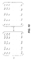
- the Image Matrix g i,j is converted into a column vector G 32. This is accomplished by converting both matrices f i,j and n i,j into column vectors by the method known as "Column stacking". Converting the matrix g i,j into the column vector G 32 results in the Optics Operator Matrix h i,j being converted into a Circulant MN x MN matrix H.
- the Circulant Matrix H is defined by a list of sub-matrices S k having the form as shown in FIGURE 10.
- the 1 st column of the matrix H is separated 34 which then enables a Fast Fourier Transform to be performed on the 1 st column of H 36.
- the Matrix D ( ⁇ ) is constructed by utilizing the vector ⁇ i 40.
- FFT is a Fast Fourier Transform
- IFFT is an inverse Fourier Transform.
- the reconstructed image (F ( ⁇ ) ) includes much of the lost special resolution which was lost due to diffraction blurring effects.
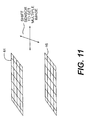
- FIGURE 11 there is shown a diagram illustrating the Multiple Image Reconstruction Technique according to the present invention.
- This technique involves taking N shifted images of a mixer grid 46 utilizing a pixel grid 44 which has been shifted against the mixer grid 46 by a known pattern of sub-pixel distances.
- the pixel grid 44 represents the image of the object.
- Each pixel is equal to the corresponding detector IFOV's, while the mixer grid 46 is a representation of the object at the desired resolution.
- E p,i represents the intensity difference of the p th pixel in the i th image between D p,i , which is equal to the measured intensity including the noise of the p th pixel in the i th image, and the contribution of the current estimate of the intensities of the mixels I m (old) .
- ⁇ I m ⁇ i ⁇ p ⁇ W m,p,i E p,i ⁇ is calculated for all mixels 54.
- ⁇ I m is the estimate of how much to change the initial mixel intensity which has been equated to I m (old) and a is an empirically chosen "convergence" parameter.
- the technique checks to see if the maximum absolute value of the mixel changes. ( ⁇ I m ) exceed the specified threshold? 56. If ⁇ I m does not exceed the threshold, the values of I m (old) are used as the best estimate of the mixer intensities.
- I m (new) I m (old) + ⁇ I m is calculated 60, where I m (new) represents new values for the mixel intensities which were calculated utilizing ⁇ I m .
- I m (new) represents new values for the mixel intensities which were calculated utilizing ⁇ I m .
- Replacing I m (old) by I m (new) 62 equates the new values for the mixel intensities with I m (old) which enables steps 52,54,56,58,60 to be repeated for these new values. This loop will be continually repeated until the values of the mixel changes ( ⁇ I m ) exceed the specified threshold as specified in step 56.
- the Non-Linear Reconstruction Technique utilizes a probability density function technique based upon the Poisson Distribution which seeks to maximize its log by utilizing an iterative process.
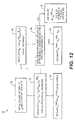
- FIGURE 13 there is shown a flow diagram of the Non--Linear Reconstruction Technique according to the present invention.
- D(j) which is I(j) (Expression 4) corrupted by noise.
- D(j) represents the actual data measured by the sensor.
- a noise suppression filter 68 is utilized to eliminate the noise which is measured by the sensors.
- a Technique to maximize L(s) with respect to S 70 is utilized to produce an output equal to the reconstructed image 72.
- step 70 the values for the particular S(i)'s must be found which maximize the expression L(s) .
- L(s) the expression that is similar to an integral equation.
- there are other techniques available to perform the maximizing of L(s) there are other techniques available to perform the maximizing of L(s) .
- the Non-Linear Multiple Band Reconstruction Technique involves combining images in different color bands of the same object in order to reproduce the image in the desired spatial resolution. As previously described, the different images are produced by modifying the sensor of the present invention according to Case three. This technique is similar to the previously described Non-Linear Reconstruction Technique, except that multi-band imaging data is utilized.
- the Non-Linear Multiple Band Reconstruction Technique also utilizes a probability density function technique based the Poisson Distribution which seeks to maximize its log by utilizing an iterative process.
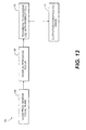
- FIGURE 14 a flow diagram of the Non-Linear Multiple Band Reconstruction Technique according to the present invention.
- D k (j) which is I k (j) (Expression 4) corrupted by noise.
- D(j) represents the actual multi-band imaging data measured by the sensor.
- noise suppression filters 80,82 are utilized to eliminate the noise in both the narrow and broad bands.
- step 84 the values for the particular S(i)'s must be found which maximize the expression L(s) . This is the same problem described in the Non-Linear Reconstruction Technique and can be solved in a similar manner.
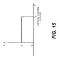
- Figure 15 shows the Fourier transform of an improved resolution image in accordance with the present invention and depicts the optical transfer function of the system and method herein. It is noted that all frequency components passed by the optical system are retained in the image, up to the cut-off frequency of the optical system.
- the present invention is not limited to any one type of optical sensor device.
- the principles which have been described herein apply to many types of applications which include, but are not limited to Optical Earth Resource Observation Systems (both Air and Spaceborne), Optical Weather Sensors (both Air and Spaceborne), Terrain Mapping Sensors (both Air and Spaceborne), Surveillance Sensors (both Air and Spaceborne), Optical Phenomenology Systems (both Air and Spaceborne), Imaging Systems that utilize optical fibers such as Medical Probes, Commercial Optical Systems such as Television Cameras, Telescopes utilized for astronomy and Optical Systems utilized for police and Rescue Work.
- the imaging device/method disclosed herein may be used on a satellite, and a means for controlling the satellite which is located on the earth may be provided.
Landscapes
- Physics & Mathematics (AREA)
- General Physics & Mathematics (AREA)
- Optics & Photonics (AREA)
- Transforming Light Signals Into Electric Signals (AREA)
Priority Applications (1)
| Application Number | Priority Date | Filing Date | Title |
|---|---|---|---|
| EP99121512A EP1096295A1 (fr) | 1999-10-28 | 1999-10-28 | Dispositif et procédé pour améliorer la résolution de capteurs optiques |
Applications Claiming Priority (1)
| Application Number | Priority Date | Filing Date | Title |
|---|---|---|---|
| EP99121512A EP1096295A1 (fr) | 1999-10-28 | 1999-10-28 | Dispositif et procédé pour améliorer la résolution de capteurs optiques |
Publications (1)
| Publication Number | Publication Date |
|---|---|
| EP1096295A1 true EP1096295A1 (fr) | 2001-05-02 |
Family
ID=8239292
Family Applications (1)
| Application Number | Title | Priority Date | Filing Date |
|---|---|---|---|
| EP99121512A Ceased EP1096295A1 (fr) | 1999-10-28 | 1999-10-28 | Dispositif et procédé pour améliorer la résolution de capteurs optiques |
Country Status (1)
| Country | Link |
|---|---|
| EP (1) | EP1096295A1 (fr) |
Cited By (2)
| Publication number | Priority date | Publication date | Assignee | Title |
|---|---|---|---|---|
| US6240219B1 (en) | 1996-12-11 | 2001-05-29 | Itt Industries Inc. | Apparatus and method for providing optical sensors with super resolution |
| EP1405346A1 (fr) * | 2001-07-06 | 2004-04-07 | Palantyr Research, LLC | Systeme et methodologie de formation d'images utilisant une configuration optique d'espace reciproque |
Citations (5)
| Publication number | Priority date | Publication date | Assignee | Title |
|---|---|---|---|---|
| US3957376A (en) * | 1974-01-25 | 1976-05-18 | International Business Machines Corporation | Measuring method and system using a diffraction pattern |
| US4093866A (en) * | 1976-04-05 | 1978-06-06 | Greenwood Mills, Inc. | Diffraction pattern amplitude analysis for use in fabric inspection |
| US4164788A (en) * | 1976-10-13 | 1979-08-14 | Atul Jain | Super-resolution imaging system |
| US4549204A (en) | 1981-11-26 | 1985-10-22 | The Secretary Of State For Defence In Her Britannic Majesty's Government Of The United Kingdom Of Great Britain And Northern Ireland | Diffraction limited imaging systems |
| US5011261A (en) | 1989-04-17 | 1991-04-30 | Photon Imaging Corp. | Color page scanner using fiber optic bundle and a photosensor array |
-
1999
- 1999-10-28 EP EP99121512A patent/EP1096295A1/fr not_active Ceased
Patent Citations (5)
| Publication number | Priority date | Publication date | Assignee | Title |
|---|---|---|---|---|
| US3957376A (en) * | 1974-01-25 | 1976-05-18 | International Business Machines Corporation | Measuring method and system using a diffraction pattern |
| US4093866A (en) * | 1976-04-05 | 1978-06-06 | Greenwood Mills, Inc. | Diffraction pattern amplitude analysis for use in fabric inspection |
| US4164788A (en) * | 1976-10-13 | 1979-08-14 | Atul Jain | Super-resolution imaging system |
| US4549204A (en) | 1981-11-26 | 1985-10-22 | The Secretary Of State For Defence In Her Britannic Majesty's Government Of The United Kingdom Of Great Britain And Northern Ireland | Diffraction limited imaging systems |
| US5011261A (en) | 1989-04-17 | 1991-04-30 | Photon Imaging Corp. | Color page scanner using fiber optic bundle and a photosensor array |
Non-Patent Citations (2)
| Title |
|---|
| M. K. SUNDARESHAN, P. ZEGERS: "Role of oversampled data in super-resolution processing and a progressive upsampling scheme for optimized implementations of iterative restoration algorithms", SPIE CONFERENCE ON PASSIVE MILLIMETER WAVE IMAGING TECHNOLOGY II, ORLANDO, FLORIDA, vol. 3703, April 1999 (1999-04-01) |
| W. R. REYNOLDS, J. W. HILGERS: "Super-resolved Imaging Sensors With Field of View Preservation", SPIE CONFERENCE ON PASSIVE MILLIMETER WAVE IMAGING TECHNOLOGY II, ORLANDO, FLORIDA, vol. 3378, April 1998 (1998-04-01) |
Cited By (4)
| Publication number | Priority date | Publication date | Assignee | Title |
|---|---|---|---|---|
| US6240219B1 (en) | 1996-12-11 | 2001-05-29 | Itt Industries Inc. | Apparatus and method for providing optical sensors with super resolution |
| EP1405346A1 (fr) * | 2001-07-06 | 2004-04-07 | Palantyr Research, LLC | Systeme et methodologie de formation d'images utilisant une configuration optique d'espace reciproque |
| EP1405346A4 (fr) * | 2001-07-06 | 2008-11-05 | Palantyr Res Llc | Systeme et methodologie de formation d'images utilisant une configuration optique d'espace reciproque |
| JP2009258746A (ja) * | 2001-07-06 | 2009-11-05 | Palantyr Research Llc | 撮像システムおよび逆空間光学設計を用いる方法 |
Similar Documents
| Publication | Publication Date | Title |
|---|---|---|
| US6240219B1 (en) | Apparatus and method for providing optical sensors with super resolution | |
| US6483952B2 (en) | Super resolution methods for electro-optical systems | |
| Rousset | Wave-front sensors | |
| Roggemann | Limited degree-of-freedom adaptive optics and image reconstruction | |
| EP1096295A1 (fr) | Dispositif et procédé pour améliorer la résolution de capteurs optiques | |
| EP1384203B1 (fr) | Procede et systeme d'amelioration de la performance d'un dispositif d'imagerie a longueur focale fixe | |
| King et al. | The current ability of HST to reveal morphological structure in medium-redshift galaxies | |
| Bracewell | Computer image processing | |
| Crampton et al. | 1343.4+ 2640-A close quasar pair | |
| Schulz | Estimation-theoretic approach to the deconvolution of atmospherically degraded images with wavefront sensor measurements | |
| White | Restoration of images and spectra from the Hubble Space Telescope | |
| Stayman et al. | An analysis of coded aperture acquisition and reconstruction using multi-frame code sequences for relaxed optical design constraints | |
| Vilnrotter et al. | An optical array receiver for deep-space communication through atmospheric turbulence | |
| Sun et al. | Image Reconstruction Based on Deep Learning for the SPIDER Optical Interferometric System | |
| Carbillet | Astronomical imaging... Atmospheric turbulence? Adaptive optics! | |
| Mugnier et al. | Inversion in optical imaging through atmospheric turbulence | |
| Fiete et al. | Image quality assessment of sparse-aperture designs with decreasing fill factors | |
| Block et al. | Image quality analysis of a spectra-radiometric sparse-aperture model | |
| WO2022158957A1 (fr) | Dispositif et procédé de détection de front d'onde à motif de diffraction codé | |
| US20220404531A1 (en) | Method and system for fabrication and use of a spectral basis filter | |
| Carlsson | Imaging physics | |
| Zhang et al. | A fast non-local means algorithm for phase diversity technique to reconstruct high-resolution multi-aperture images | |
| Gerwe et al. | Comparison of maximum-likelihood image and wavefront reconstruction using conventional image, phase diversity, and lenslet diversity data | |
| Kupke et al. | Wavefront curvature sensing on extended arbitrary scenes: simulation results | |
| Noyola et al. | experimental Demonstration of Adaptive Infrared Multispectral Imaging using plasmonic Filter Array |
Legal Events
| Date | Code | Title | Description |
|---|---|---|---|
| PUAI | Public reference made under article 153(3) epc to a published international application that has entered the european phase |
Free format text: ORIGINAL CODE: 0009012 |
|
| AK | Designated contracting states |
Kind code of ref document: A1 Designated state(s): DE FR GB |
|
| AX | Request for extension of the european patent |
Free format text: AL;LT;LV;MK;RO;SI |
|
| 17P | Request for examination filed |
Effective date: 20011031 |
|
| AKX | Designation fees paid |
Free format text: DE FR GB |
|
| 17Q | First examination report despatched |
Effective date: 20040715 |
|
| APBK | Appeal reference recorded |
Free format text: ORIGINAL CODE: EPIDOSNREFNE |
|
| APBN | Date of receipt of notice of appeal recorded |
Free format text: ORIGINAL CODE: EPIDOSNNOA2E |
|
| APBR | Date of receipt of statement of grounds of appeal recorded |
Free format text: ORIGINAL CODE: EPIDOSNNOA3E |
|
| APAF | Appeal reference modified |
Free format text: ORIGINAL CODE: EPIDOSCREFNE |
|
| APBT | Appeal procedure closed |
Free format text: ORIGINAL CODE: EPIDOSNNOA9E |
|
| RAP1 | Party data changed (applicant data changed or rights of an application transferred) |
Owner name: EXELIS INC. |
|
| STAA | Information on the status of an ep patent application or granted ep patent |
Free format text: STATUS: THE APPLICATION HAS BEEN REFUSED |
|
| 18R | Application refused |
Effective date: 20130404 |