EP1094554A2 - Connector - Google Patents
Connector Download PDFInfo
- Publication number
- EP1094554A2 EP1094554A2 EP00402865A EP00402865A EP1094554A2 EP 1094554 A2 EP1094554 A2 EP 1094554A2 EP 00402865 A EP00402865 A EP 00402865A EP 00402865 A EP00402865 A EP 00402865A EP 1094554 A2 EP1094554 A2 EP 1094554A2
- Authority
- EP
- European Patent Office
- Prior art keywords
- memory module
- connector
- connection object
- slider
- key
- Prior art date
- Legal status (The legal status is an assumption and is not a legal conclusion. Google has not performed a legal analysis and makes no representation as to the accuracy of the status listed.)
- Granted
Links
Images



Classifications
-
- H—ELECTRICITY
- H01—ELECTRIC ELEMENTS
- H01R—ELECTRICALLY-CONDUCTIVE CONNECTIONS; STRUCTURAL ASSOCIATIONS OF A PLURALITY OF MUTUALLY-INSULATED ELECTRICAL CONNECTING ELEMENTS; COUPLING DEVICES; CURRENT COLLECTORS
- H01R12/00—Structural associations of a plurality of mutually-insulated electrical connecting elements, specially adapted for printed circuits, e.g. printed circuit boards [PCB], flat or ribbon cables, or like generally planar structures, e.g. terminal strips, terminal blocks; Coupling devices specially adapted for printed circuits, flat or ribbon cables, or like generally planar structures; Terminals specially adapted for contact with, or insertion into, printed circuits, flat or ribbon cables, or like generally planar structures
- H01R12/70—Coupling devices
- H01R12/71—Coupling devices for rigid printing circuits or like structures
- H01R12/72—Coupling devices for rigid printing circuits or like structures coupling with the edge of the rigid printed circuits or like structures
- H01R12/722—Coupling devices for rigid printing circuits or like structures coupling with the edge of the rigid printed circuits or like structures coupling devices mounted on the edge of the printed circuits
- H01R12/725—Coupling devices for rigid printing circuits or like structures coupling with the edge of the rigid printed circuits or like structures coupling devices mounted on the edge of the printed circuits containing contact members presenting a contact carrying strip, e.g. edge-like strip
-
- H—ELECTRICITY
- H01—ELECTRIC ELEMENTS
- H01R—ELECTRICALLY-CONDUCTIVE CONNECTIONS; STRUCTURAL ASSOCIATIONS OF A PLURALITY OF MUTUALLY-INSULATED ELECTRICAL CONNECTING ELEMENTS; COUPLING DEVICES; CURRENT COLLECTORS
- H01R13/00—Details of coupling devices of the kinds covered by groups H01R12/70 or H01R24/00 - H01R33/00
Definitions
- the present invention relates to a connector for electrically connecting a connection object, such as a memory module, to a terminal and, more particularly, to a connector having the ability to prevent erroneous loading of the connection object.
- the memory module When the memory module is loaded to the connector having these latches, the memory module is inserted in the connector at a predetermined angle until contacts on the connector and conductive pads on the memory module are brought into contact with each other and then the memory module is tilted down toward the connector. Then, the protrusions of the latches and the cutouts of the memory module are engaged with each other and thereby the memory module is fixed to the connector.
- a user When the memory module is released or unloaded from the connector, a user have to pull out the memory module from its loaded position, manipulating the ears to move the latches in a direction of being laterally spaced from each other.
- the structure of the main body can be shared with different types of connection object. This can allow the connector to accommodate two or more types of connection objects by simply replacing the auxiliary member.
- connection object is connected to the terminal by moving the operating member after the connection object is supported on the auxiliary member in the non-connected state, a user can simply switch between the connected mode and the non-connected mode of the connection object in a simple manner by the operation of the single operating member. Also, there is no need for a user to directly touch the connection object when the connection object is switched between the connected mode and the non-connected mode, so that local application of an excessive force to the connection object or the connector can be avoided and, thus, the damage or deformation of these components can be prevented.
- the uneven parts and the fitting parts are not necessarily required to have an identical configuration among themselves.
- those two fitting parts may be different in configuration from each other.
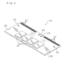
- a memory module 30 shown in FIG. 3 is of generally rectangular in plan configuration, and on both sides thereof a plurality of chips 31 including DRAM chips are mounted.
- the memory module has two key slots (uneven parts) 33, 34 around a center part thereof on the front side in the direction of its being inserted into the connector 1 and a large number of conductive pads 32 on front and back faces thereof at both lateral sides of the key slots.
- the key slot 33 is in the form of a recess having a semicircular form at a tip end thereof.
- the key slot 34 has the same size and configuration as the key slot 33.
- Cutouts 36 are provided at opposite ends of the memory module 30, respectively. The cutouts 36 are for permitting the memory module 30 to be loaded to the connector having the latches.
- the location where the key 25 is formed varies right and left according to the location where the key slot 34 of the memory module 30 is formed.
- the arms 23a, 23b have bent portions 26 bent upward at positions close to the ends and columnar protrusions 27 formed outside of the bent portions.
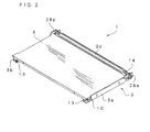
- the cover 6 made of metallic material is formed to have a size to cover the whole area of the memory module 30 when the cover is closed, as shown in FIG. 2.
- the cover 6 is provided at both ends thereof with bent portions 10 bent toward the base 3, respectively.
- the bent portions 10 are provided at inside thereof with the protrusions 11 which are brought into engagement with the recesses 12 in the arms 3a, 3b of the base 3 when the cover 6 is closed.
- the cover 6 has two bent arms 28a, 28b which are bent inwardly toward the ends at portions thereof opposite the bent portions 10 at the both ends of the cover 6.
- the bent arms 28a, 28b are rotatably connected with the shaft 14 in a rotatable relation at portions thereof close to the bent portions.
- the bent arms 28a, 28b have generally elliptical holes 29 formed near the ends thereof.
- the columnar protrusions 27 of the slider 5 are fitted in the holes 29 and thereby the slider 5 and the cover 6 are rotatably connected.
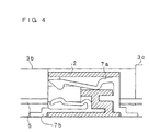
- the memory module 30 When the connector 1 of this embodiment is loaded with the memory module 30, the memory module 30 is put on the slider 5, with the cover 6 opened, so that it can be supported thereon, as shown in FIG. 7. At that time, the slider 5 is in its shifted position away from the housing 2, so that the memory module 30 can be put on the slider 5 with comparative ease. For putting the memory module 30 on and thus supported by the slider 5, it is only necessary that the projections 24 on the slider 5 are inserted into the holes 35 in the memory module 30. At that time, the memory module 30 is away from the housing 2 and the conductive pads 32 are not in contact with the upper and lower contacts 7a, 7b, as shown in FIG. 8(a). At the same time as the memory module 30 is supported on the slider 5, the key 25 of the slider is fitted in the key slot 34 of the memory module 30.
- the slider 5 having the key 25 to fit in the key slot 34 formed in the memory module 30 at a location that differs according to the operating voltage is mounted on the main body 4, only the memory module 30 having the key slot 34 corresponding in position to the key 25 formed in the slider 5 can be loaded to the connector 1. Hence, the erroneous loading of the memory module 30 to the connector 1 can be prevented.
- the memory module 30 is connected to the contacts 7a, 7b by rotating the cover 6 after the memory module 30 is supported on the slider 5 in the state in which the cover 6 is opened.
- the manual operation of the cover 6 can permit the selective switching between the connected mode of the memory module 30 and the non-connected mode of the same in a simple manner.
- the two keys 16, 25 to fit in the two key slots 33, 34 formed in the memory module 30 are separated and arranged one on each of the main body 4 and the slider 5. This can produce the result that after the fitting engagement of the key slot 34 of the memory module 30 and the key 25 of the slider 5, the slider 5 is moved toward the housing 2 and thereby the fitting engagement of another key slot 33 of the memory module 30 and the key 16 of the main body 4 can be achieved. As a result of this, it is only necessary for supporting the memory module 30 to the slider 5 to align the memory module 30 so that the fitting engagement of the key slot 34 of the memory module 30 and the key 25 of the slider 5 can be achieved.
- the two keys 16, 25 are separated and arranged one on each of the main body 4 and the slider 5 and, thus, only a single key is formed on each of the housing 2 and the slider 5.
- This can produce the advantage that the fitting engagement of the key slots 33, 34 and the keys 16, 25 can easily be achieved without requiring high degree of manufacturing accuracy for the housing 2 and the slider 5 such that the keys 16, 25 can accurately be positioned, when compared with the manufacturing accuracy required for the two keys 16, 25 to be both formed in the housing 2.
- the memory module 30 can be loaded in place without applying a relatively large force to the memory module to press it in against the elasticity of coil springs, the loading work of the memory module can be performed with ease. Further, no elastic members such as coil springs are required, thus yielding a simplified structure and reduced manufacturing costs.
- the whole area of the memory module 30 is covered with the cover 6, so that the memory module 30 can be protected from dust when connected therewith. Therefore, malfunction caused by loose connection or short circuit can be prevented effectively.
- the cover 6 Since the cover 6 is made of metallic material, even when unwanted electromagnetic waves are produced from the memory module 30 or a connecting part between the memory module and the contacts 7a, 7b, it can shield the electromagnetic waves not to let them leak out. Also, since electromagnetic waves from outside can be shielded by the cover 6, the operation of the memory module 30 can be prevented from being adversely affected by the electromagnetic waves from outside.
- the cover 6 since the cover 6 is rotated around the shaft 14 extending substantially in parallel to the bearing surface for the memory module 30, the cover 6 does not protrude outside of a plane area defined by the cover 6 when the memory module 30 and the contacts 7a, 7b are contacted with each other (i.e., when the cover 6 is closed). Therefore, even when an extra space is not found at the outside of the plane area, the connection between the memory module 30 and the contacts 7a, 7b can be realized by rotating the cover 6.
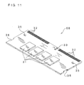
- a memory module 68 shown in FIG. 11 is only different from the memory module 30 shown in FIG. 3 in that it has only a single alignment-use key slot 33.
- a connector 60 of this embodiment is only different from the connector 1 shown in FIG. 1 in that it has a key 25c formed at such a position as to fit in the key slot 33 and has a configuration to fit in the same key slot 33 and that the key 16 shown in FIG. 1 is not arranged in the housing 52.
Landscapes
- Details Of Connecting Devices For Male And Female Coupling (AREA)
- Coupling Device And Connection With Printed Circuit (AREA)
Abstract
Description
Claims (3)
- A connector (1) for electrically connecting a connection object (30) and a terminal (7a,7b), characterized by comprising:a main body (4);said terminal (7a,7b), arranged at said main body (4), to be electrically connected with said connection object (30) having at least one uneven part (34); andan auxiliary member (5) mounted on said main body (4) and having at least one fitting part (25) to fit to the respective of said at least one uneven part (34) of said connection object (30).
- A connector (1) according to claim 1, characterized by further comprising an operating member (6) mounted on said main body (4) to be associated therewith, and in which said auxiliary member (5) is adapted to detachably support said connection object (30) and to move reciprocally relative to said terminal (7a.7b) in association with movement of said operating member (6).
- A connector (1) according to claim 2, characterized in that two or more fitting parts (16,25) to fit to their related two or more uneven parts (33,34) formed in said connection object (30) are separately arranged so that each of said main body (4) and said auxiliary member (5) has at least one fitting part (16,25).
Applications Claiming Priority (2)
| Application Number | Priority Date | Filing Date | Title |
|---|---|---|---|
| JP29522899A JP2001118619A (en) | 1999-10-18 | 1999-10-18 | connector |
| JP29522899 | 1999-10-18 |
Publications (3)
| Publication Number | Publication Date |
|---|---|
| EP1094554A2 true EP1094554A2 (en) | 2001-04-25 |
| EP1094554A3 EP1094554A3 (en) | 2001-10-10 |
| EP1094554B1 EP1094554B1 (en) | 2003-07-23 |
Family
ID=17817880
Family Applications (1)
| Application Number | Title | Priority Date | Filing Date |
|---|---|---|---|
| EP00402865A Expired - Lifetime EP1094554B1 (en) | 1999-10-18 | 2000-10-16 | Connector |
Country Status (7)
| Country | Link |
|---|---|
| US (1) | US6428338B1 (en) |
| EP (1) | EP1094554B1 (en) |
| JP (1) | JP2001118619A (en) |
| KR (1) | KR100485501B1 (en) |
| CN (1) | CN100359767C (en) |
| DE (1) | DE60003993T2 (en) |
| TW (1) | TW469672B (en) |
Families Citing this family (14)
| Publication number | Priority date | Publication date | Assignee | Title |
|---|---|---|---|---|
| GB2365718B (en) * | 2000-08-01 | 2002-04-17 | 3Com Corp | Cascade architecture and operation for packet-based communication systems |
| US6558186B1 (en) * | 2001-10-11 | 2003-05-06 | Molex Incorporated | Keyed connector assembly for flat flexible circuitry |
| US7300298B2 (en) * | 2002-12-27 | 2007-11-27 | Fci | Board securing device |
| TW573829U (en) * | 2003-06-17 | 2004-01-21 | Molex Taiwan Ltd | Electrical card connector |
| JP4909510B2 (en) * | 2004-12-20 | 2012-04-04 | 株式会社東芝 | Electronics |
| TWM278118U (en) * | 2005-05-30 | 2005-10-11 | Tai Sol Electronics Co Ltd | Card connector having terminal selection effect |
| KR100935778B1 (en) * | 2006-08-03 | 2010-01-06 | 니혼 고꾸 덴시 고교 가부시끼가이샤 | Easily Adapted Connectors for Miniaturization |
| US7751199B2 (en) | 2006-09-11 | 2010-07-06 | Apple Inc. | Support tabs for protecting a circuit board from applied forces |
| US7381074B1 (en) * | 2006-12-19 | 2008-06-03 | International Business Machines Corporation | Locking and activation mechanism for a hot swappable daughter card |
| TWM360483U (en) * | 2008-09-30 | 2009-07-01 | Hon Hai Prec Ind Co Ltd | Electrical connector |
| JP2010225183A (en) * | 2010-07-02 | 2010-10-07 | Toshiba Corp | Electronics |
| JP5634179B2 (en) * | 2010-09-09 | 2014-12-03 | 日本航空電子工業株式会社 | Holding member and assembly |
| US9203187B2 (en) * | 2014-04-08 | 2015-12-01 | Aic Inc. | Hot plug structure of electronic peripheral device |
| CN113285301B (en) * | 2021-05-19 | 2023-06-30 | 菲尼克斯亚太电气(南京)有限公司 | Locking device, unlocking device and locking and unlocking assembly |
Family Cites Families (18)
| Publication number | Priority date | Publication date | Assignee | Title |
|---|---|---|---|---|
| CA1204213A (en) * | 1982-09-09 | 1986-05-06 | Masahiro Takeda | Memory card having static electricity protection |
| JPH0719628B2 (en) * | 1985-07-12 | 1995-03-06 | 富士通株式会社 | connector |
| US4887188A (en) * | 1987-12-22 | 1989-12-12 | Casio Computer Co., Ltd. | Connector for a memory card |
| JPH01248877A (en) * | 1988-03-30 | 1989-10-04 | Fuji Photo Film Co Ltd | Attaching/detaching device for memory cartridge |
| GB2257580B (en) | 1991-07-02 | 1995-10-04 | Amp Inc | Electronic module socket with resilient latch |
| US5325263A (en) * | 1991-07-22 | 1994-06-28 | Silicon Graphics, Inc. | Rack and pinion retaining and release device for removable computer components |
| US5483419A (en) * | 1991-09-24 | 1996-01-09 | Teac Corporation | Hot-swappable multi-cartridge docking module |
| JP2541694Y2 (en) * | 1991-12-27 | 1997-07-16 | ケル株式会社 | Memory card connector with ejection mechanism |
| US5207598A (en) * | 1992-02-24 | 1993-05-04 | Molex Incorporated | Edge card connector |
| JPH0789282A (en) * | 1993-06-30 | 1995-04-04 | Mitsubishi Electric Corp | IC memory card, host device side connector and connection system using them |
| JPH07122057A (en) | 1993-10-22 | 1995-05-12 | Ricoh Co Ltd | Recording disk drive |
| JP2717364B2 (en) | 1994-09-30 | 1998-02-18 | 日本航空電子工業株式会社 | connector |
| JP2809339B2 (en) | 1995-03-10 | 1998-10-08 | ケル株式会社 | Edge connector |
| US5580257A (en) * | 1995-04-28 | 1996-12-03 | Molex Incorporated | High performance card edge connector |
| US5689405A (en) * | 1996-09-25 | 1997-11-18 | Itt Corporation | IC card rear board support |
| JP3248068B2 (en) * | 1997-10-27 | 2002-01-21 | ホシデン株式会社 | Card connector |
| JP3050192B2 (en) * | 1997-11-12 | 2000-06-12 | 日本電気株式会社 | Card edge connector, electronic equipment |
| GB2339080A (en) * | 1998-06-29 | 2000-01-12 | Havant International Ltd | Mounting and testing of electrical devices such as disc drives |
-
1999
- 1999-10-18 JP JP29522899A patent/JP2001118619A/en active Pending
-
2000
- 2000-10-07 TW TW089121038A patent/TW469672B/en active
- 2000-10-16 DE DE60003993T patent/DE60003993T2/en not_active Expired - Fee Related
- 2000-10-16 EP EP00402865A patent/EP1094554B1/en not_active Expired - Lifetime
- 2000-10-18 KR KR10-2000-0061396A patent/KR100485501B1/en not_active Expired - Fee Related
- 2000-10-18 CN CNB001314351A patent/CN100359767C/en not_active Expired - Fee Related
- 2000-10-18 US US09/690,463 patent/US6428338B1/en not_active Expired - Lifetime
Also Published As
| Publication number | Publication date |
|---|---|
| EP1094554A3 (en) | 2001-10-10 |
| KR100485501B1 (en) | 2005-04-27 |
| DE60003993T2 (en) | 2004-05-27 |
| KR20010040125A (en) | 2001-05-15 |
| DE60003993D1 (en) | 2003-08-28 |
| JP2001118619A (en) | 2001-04-27 |
| US6428338B1 (en) | 2002-08-06 |
| CN1293469A (en) | 2001-05-02 |
| TW469672B (en) | 2001-12-21 |
| CN100359767C (en) | 2008-01-02 |
| EP1094554B1 (en) | 2003-07-23 |
Similar Documents
| Publication | Publication Date | Title |
|---|---|---|
| EP1094554B1 (en) | Connector | |
| US6480390B2 (en) | Card-type peripheral device | |
| KR100682570B1 (en) | Adapter for Memory Card | |
| US5299089A (en) | Connector device having two storage decks and three contact arrays for one hard disk drive package or two memory cards | |
| EP1860743B1 (en) | Card connector and method for producing housing assembly | |
| US6544061B1 (en) | Connector with slide | |
| US6226189B1 (en) | Data card housing | |
| US7616447B2 (en) | IC card | |
| JP2001160458A (en) | Card connector | |
| US20070243732A1 (en) | Rotatable memory card with improved locking mechanism | |
| US20080041952A1 (en) | Subscriber identity module card and method of recognizing the same | |
| JP2000021475A (en) | Ic card connector | |
| CN108336525B (en) | Card seat assembly and electronic equipment | |
| EP1146473B1 (en) | Card connector | |
| US20070218770A1 (en) | Card connector | |
| EP1143371B1 (en) | Electrical connector | |
| US7033222B2 (en) | Card-receiving device | |
| JP2001102136A (en) | Electronic device connection device, USB connection device, and electronic device with coupling mechanism | |
| KR20220014568A (en) | Bidirectional ic card socket | |
| CN100435427C (en) | Electronic apparatus which requires less space for loading and unloading an object | |
| US20070131778A1 (en) | Chip card retaining mechanism | |
| US20240155797A1 (en) | Printed circuit board card retention | |
| JP4701995B2 (en) | connector |
Legal Events
| Date | Code | Title | Description |
|---|---|---|---|
| PUAI | Public reference made under article 153(3) epc to a published international application that has entered the european phase |
Free format text: ORIGINAL CODE: 0009012 |
|
| AK | Designated contracting states |
Kind code of ref document: A2 Designated state(s): AT BE CH CY DE DK ES FI FR GB GR IE IT LI LU MC NL PT SE Kind code of ref document: A2 Designated state(s): DE FR GB |
|
| AX | Request for extension of the european patent |
Free format text: AL;LT;LV;MK;RO;SI |
|
| PUAL | Search report despatched |
Free format text: ORIGINAL CODE: 0009013 |
|
| AK | Designated contracting states |
Kind code of ref document: A3 Designated state(s): AT BE CH CY DE DK ES FI FR GB GR IE IT LI LU MC NL PT SE |
|
| AX | Request for extension of the european patent |
Free format text: AL;LT;LV;MK;RO;SI |
|
| RIC1 | Information provided on ipc code assigned before grant |
Free format text: 7H 01R 12/18 A, 7H 05K 7/14 B |
|
| 17P | Request for examination filed |
Effective date: 20020314 |
|
| 17Q | First examination report despatched |
Effective date: 20020523 |
|
| AKX | Designation fees paid |
Free format text: DE FR GB |
|
| GRAH | Despatch of communication of intention to grant a patent |
Free format text: ORIGINAL CODE: EPIDOS IGRA |
|
| GRAH | Despatch of communication of intention to grant a patent |
Free format text: ORIGINAL CODE: EPIDOS IGRA |
|
| GRAA | (expected) grant |
Free format text: ORIGINAL CODE: 0009210 |
|
| AK | Designated contracting states |
Designated state(s): DE FR GB |
|
| REG | Reference to a national code |
Ref country code: GB Ref legal event code: FG4D |
|
| REF | Corresponds to: |
Ref document number: 60003993 Country of ref document: DE Date of ref document: 20030828 Kind code of ref document: P |
|
| ET | Fr: translation filed | ||
| PLBE | No opposition filed within time limit |
Free format text: ORIGINAL CODE: 0009261 |
|
| STAA | Information on the status of an ep patent application or granted ep patent |
Free format text: STATUS: NO OPPOSITION FILED WITHIN TIME LIMIT |
|
| 26N | No opposition filed |
Effective date: 20040426 |
|
| PGFP | Annual fee paid to national office [announced via postgrant information from national office to epo] |
Ref country code: FR Payment date: 20060816 Year of fee payment: 7 |
|
| PGFP | Annual fee paid to national office [announced via postgrant information from national office to epo] |
Ref country code: GB Payment date: 20061002 Year of fee payment: 7 |
|
| PGFP | Annual fee paid to national office [announced via postgrant information from national office to epo] |
Ref country code: DE Payment date: 20061009 Year of fee payment: 7 |
|
| GBPC | Gb: european patent ceased through non-payment of renewal fee |
Effective date: 20071016 |
|
| PG25 | Lapsed in a contracting state [announced via postgrant information from national office to epo] |
Ref country code: DE Free format text: LAPSE BECAUSE OF NON-PAYMENT OF DUE FEES Effective date: 20080501 |
|
| REG | Reference to a national code |
Ref country code: FR Ref legal event code: ST Effective date: 20080630 |
|
| PG25 | Lapsed in a contracting state [announced via postgrant information from national office to epo] |
Ref country code: GB Free format text: LAPSE BECAUSE OF NON-PAYMENT OF DUE FEES Effective date: 20071016 |
|
| PG25 | Lapsed in a contracting state [announced via postgrant information from national office to epo] |
Ref country code: FR Free format text: LAPSE BECAUSE OF NON-PAYMENT OF DUE FEES Effective date: 20071031 |