EP1094369A2 - Image forming apparatus - Google Patents
Image forming apparatus Download PDFInfo
- Publication number
- EP1094369A2 EP1094369A2 EP00122868A EP00122868A EP1094369A2 EP 1094369 A2 EP1094369 A2 EP 1094369A2 EP 00122868 A EP00122868 A EP 00122868A EP 00122868 A EP00122868 A EP 00122868A EP 1094369 A2 EP1094369 A2 EP 1094369A2
- Authority
- EP
- European Patent Office
- Prior art keywords
- image
- toner
- bearing member
- image forming
- image bearing
- Prior art date
- Legal status (The legal status is an assumption and is not a legal conclusion. Google has not performed a legal analysis and makes no representation as to the accuracy of the status listed.)
- Granted
Links
- 238000012546 transfer Methods 0.000 claims abstract description 29
- 239000000463 material Substances 0.000 claims abstract description 8
- 230000015572 biosynthetic process Effects 0.000 claims description 9
- 238000004140 cleaning Methods 0.000 claims description 5
- 239000002245 particle Substances 0.000 claims 2
- 238000000034 method Methods 0.000 description 17
- 238000012545 processing Methods 0.000 description 15
- 238000001444 catalytic combustion detection Methods 0.000 description 12
- 238000010276 construction Methods 0.000 description 8
- 230000008569 process Effects 0.000 description 8
- 238000007599 discharging Methods 0.000 description 5
- 230000005611 electricity Effects 0.000 description 5
- 230000000873 masking effect Effects 0.000 description 5
- 238000006243 chemical reaction Methods 0.000 description 4
- 230000006835 compression Effects 0.000 description 4
- 238000007906 compression Methods 0.000 description 4
- 238000012937 correction Methods 0.000 description 4
- 238000010586 diagram Methods 0.000 description 4
- 239000011521 glass Substances 0.000 description 4
- 230000000284 resting effect Effects 0.000 description 4
- 230000008859 change Effects 0.000 description 3
- 238000001514 detection method Methods 0.000 description 2
- 238000009434 installation Methods 0.000 description 2
- 230000003595 spectral effect Effects 0.000 description 2
- 229910000859 α-Fe Inorganic materials 0.000 description 2
- 230000009471 action Effects 0.000 description 1
- 230000004075 alteration Effects 0.000 description 1
- 238000003705 background correction Methods 0.000 description 1
- 239000003086 colorant Substances 0.000 description 1
- 230000003111 delayed effect Effects 0.000 description 1
- 238000011161 development Methods 0.000 description 1
- 230000000694 effects Effects 0.000 description 1
- 238000009499 grossing Methods 0.000 description 1
- 229910052736 halogen Inorganic materials 0.000 description 1
- 150000002367 halogens Chemical class 0.000 description 1
- 238000012986 modification Methods 0.000 description 1
- 230000004048 modification Effects 0.000 description 1
- 230000009467 reduction Effects 0.000 description 1
- 238000000926 separation method Methods 0.000 description 1
- 239000007787 solid Substances 0.000 description 1
- 239000000758 substrate Substances 0.000 description 1
- 230000001360 synchronised effect Effects 0.000 description 1
Images




Classifications
-
- G—PHYSICS
- G03—PHOTOGRAPHY; CINEMATOGRAPHY; ANALOGOUS TECHNIQUES USING WAVES OTHER THAN OPTICAL WAVES; ELECTROGRAPHY; HOLOGRAPHY
- G03G—ELECTROGRAPHY; ELECTROPHOTOGRAPHY; MAGNETOGRAPHY
- G03G21/00—Arrangements not provided for by groups G03G13/00 - G03G19/00, e.g. cleaning, elimination of residual charge
- G03G21/0005—Arrangements not provided for by groups G03G13/00 - G03G19/00, e.g. cleaning, elimination of residual charge for removing solid developer or debris from the electrographic recording medium
- G03G21/0064—Arrangements not provided for by groups G03G13/00 - G03G19/00, e.g. cleaning, elimination of residual charge for removing solid developer or debris from the electrographic recording medium using the developing unit, e.g. cleanerless or multi-cycle apparatus
-
- G—PHYSICS
- G03—PHOTOGRAPHY; CINEMATOGRAPHY; ANALOGOUS TECHNIQUES USING WAVES OTHER THAN OPTICAL WAVES; ELECTROGRAPHY; HOLOGRAPHY
- G03G—ELECTROGRAPHY; ELECTROPHOTOGRAPHY; MAGNETOGRAPHY
- G03G15/00—Apparatus for electrographic processes using a charge pattern
- G03G15/02—Apparatus for electrographic processes using a charge pattern for laying down a uniform charge, e.g. for sensitising; Corona discharge devices
- G03G15/0208—Apparatus for electrographic processes using a charge pattern for laying down a uniform charge, e.g. for sensitising; Corona discharge devices by contact, friction or induction, e.g. liquid charging apparatus
- G03G15/0216—Apparatus for electrographic processes using a charge pattern for laying down a uniform charge, e.g. for sensitising; Corona discharge devices by contact, friction or induction, e.g. liquid charging apparatus by bringing a charging member into contact with the member to be charged, e.g. roller, brush chargers
-
- G—PHYSICS
- G03—PHOTOGRAPHY; CINEMATOGRAPHY; ANALOGOUS TECHNIQUES USING WAVES OTHER THAN OPTICAL WAVES; ELECTROGRAPHY; HOLOGRAPHY
- G03G—ELECTROGRAPHY; ELECTROPHOTOGRAPHY; MAGNETOGRAPHY
- G03G2221/00—Processes not provided for by group G03G2215/00, e.g. cleaning or residual charge elimination
- G03G2221/0005—Cleaning of residual toner
Definitions
- the present invention relates to an image forming apparatus such as a copying machine, a printer and the like, utilizing an electrophotographic system or an electrostatic recording system.
- Image forming apparatuses utilizing an electrophotographic system are well-known.
- an image forming process of such an apparatus after a surface of a photosensitive drum as a latent image bearing member is uniformly charged by a charging device, an electrostatic latent image is formed on the photosensitive drum by a laser or an LED. Then, the electrostatic latent image is developed with toner as developer to form a toner image which is in turn transferred onto a recording material as a recording medium such as paper.
- color image formation the above-mentioned process is repeated for magenta, cyan, yellow and black colors, and color toner images superimposed on the recording material is fixed to the recording material by heat to form a color image.
- this process after the transferring, residual toner remaining on the photosensitive drum is removed by an exclusive cleaning apparatus.
- transfer-residual toner In such a cleaner-less image forming apparatus, after the transferring, in order to remove the residual toner remaining on the photosensitive drum (referred to as "transfer-residual toner" hereinafter), for example, there has been proposed a method in which, after the transferring, a small amount of toner remaining on the photosensitive drum is once received by the charging device as charging means of contact type to change the electrostatic property and then the toner is returned to the photosensitive drum again, and, thereafter, the toner is collected by a developing apparatus also acting as collecting means to use the toner again.
- the residual toner on the surface of the photosensitive drum is removed and collected in a sheet-to-sheet interval during the print job or within a predetermined time period after the print job.
- Such a method is described in the Applicant's U.S. Patent Application Serial No. 219,602 (filed on December 23, 1998).
- An object of the present invention is to provide an image forming apparatus in which collection and discharging of toner can be effected without worsening a charging ability of a charging device.
- Another object of the present invention is to provide an image forming apparatus in which a discharging time from charging means can be altered.
- a further object of the present invention is to provide an image forming apparatus comprising an image bearing member, charging means for charging the image bearing member, electrostatic image forming means for selectively removing charges on the image bearing member charged by the charging means to form an electrostatic image, developing means for developing the electrostatic image with toner as a toner image, transfer means for transferring the toner image on the image bearing member onto a transfer material (the charging means temporarily collecting residual toner after the transferring), return bias applying means for applying a return bias for returning the toner collected in the charging means to the image bearing member in a non-image forming period, and control means for controlling a return bias applying time period of the return bias applying means.
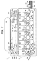
- Fig. 1 is a sectional view showing a schematic construction of a color image forming apparatus as an example of an image forming apparatus according to an embodiment of the present invention.
- Such a color image forming apparatus includes a color reader portion 1 and a color printer portion 2.
- an original resting glass (platen) 301 is located at an upper portion, and an original feeding apparatus (DF) 302 is provided above the original resting glass.
- a mirror surface pressing plate may be mounted.
- light sources 303 and 304 as halogen lamps, reflection hoods 305 and 306 for collecting lights from the light sources 303 and 304 onto the original, and a reflection mirror 307 for reflecting reflection light or projection light from the original.
- mirrors 308 and 309 for collecting the reflection light from the mirror 307 onto a CCD 101.
- the color reader portion 1 further comprises a digital image processing portion (referred to as "image processing portion” hereinafter) 312 including a substrate 311 on which the CCD 101 is mounted, elements shown in Fig. 2 other than the CCD 101, and a binary value converting portion 201 and delay portions 202, 203 and 204 as shown in Fig. 3, and an interface (I/F) portion 313 to other elements such as an IPU.
- image processing portion referred to as "image processing portion” hereinafter
- image processing portion 312 including a substrate 311 on which the CCD 101 is mounted, elements shown in Fig. 2 other than the CCD 101, and a binary value converting portion 201 and delay portions 202, 203 and 204 as shown in Fig. 3, and an interface (I/F) portion 313 to other elements such as an IPU.
- first carriage 314 and the second carriage 315 are mechanically shifted at speeds of V and V/2, respectively by driving means 316 in a direction perpendicular to an electrical scanning direction (main scanning direction) of the CCD 101, thereby scanning (sub-scanning) the entire surface of the original.
- Fig. 2 is a block diagram showing the image processing portion 312 in detail.
- the lights from the light sources 303 and 304 are reflected by the original rested on the original resting glass 301, and the reflected lights are directed to the CCD 101, where the lights are converted into electric signals.
- the CCD 101 may be constituted so that R (red), G (green) and B (blue) color filters are arranged in-line CCD in the order of R, G and B or may be constituted so that the R filter, G filter and B filter are arranged on three CCDs, respectively or may be constituted so that the filters are designed as on-chip or the filters are provided independently of the CCDs.
- the electric signals are inputted to the image processing portion 312, sample hold (S/H) is effected in a clamp & Amp. & S/H & A/D portion 102, so that dark levels of the analogue image signals are clamped to reference potentials and amplified to predetermined amounts (processing order is not necessarily the above-mentioned order) and A/D-converted thereby to be converted into R, G and B 8-bit digital signals, for example.
- S/H sample hold
- shading correction and black correction of the R, G and B signals are effected in a shading portion 103.
- the CCD 101 is three-line CCD
- MTF correction since MTF readings are changed in accordance with the reading speeds and variable power rates, which changes are corrected. Further, a size of the original on the original resting glass is ascertained by original detection.
- the digital signals the reading position timings of which are corrected are inputted to an input masking portion 105, where a spectral property of the CCD 101 and spectral properties of the light sources 303, 304 and the reflection hoods 305, 306 are corrected.
- Output from the input masking portion 105 is inputted to a selector 106 which can be switched to an external I/F signal.
- the signals outputted from the selector 106 are inputted to a color space compression & undercolor (under color) removal & LOG conversion portion 107 and an undercolor removing portion 115.
- This signals inputted to the undercolor removing portion 115, where undercolor is removed, are then inputted to a black character judging portion 116 for judging whether characters on the original are black or not, where a black character signal is formed from the original.
- a black character signal is formed from the original.
- the color space compression & undercolor removal & LOG conversion portion 107 into which the output of the selector 106 was inputted by color space compression, it is judged whether the read image signals are within a range in which the image signals can be reproduced by the printer. If the signals are within such a range, the signals are not processed; whereas, if the signals are not within such a range, the signals are corrected so that the signals fall within the range in which the image signals can be reproduced by the printer. Then, the undercolor removing process is performed, and, by LOG conversion, the R, G and B signals are converted into C (cyan), M (magenta) and Y (yellow) signals.
- the output signals from the color space compression & undercolor removal & LOG conversion portion 107 are inputted to a delay portion 108, where the timing is adjusted.
- the two kinds of signals are inputted to a moire removing portion 109, where moire is removed.
- the signals are inputted to a variable power processing portion 110, where variable power processing is effected in the main scanning direction.
- C, M, Y and K (black) signals are formed from the C, M and Y signals by UCR processing, and the signals are corrected to signals suitable for the output of the printer by masking processing, and the judging signal formed in the black character judging portion 116 is fed-back to the C, M, Y and K signals.
- the signals processed in the UCR & masking & black character reflecting portion 111 are inputted to a ⁇ correction portion 12, where density is adjusted. Then, in a filter portion 113, smoothing or edge processing is effected.
- this converting method may be a deza method, an error diffusing method or an improved error diffusing method.
- the color printer portion 2 comprises a Y image forming portion 317, an M image forming portion 318, a C image forming portion 319 and a K image forming portion 320, and these portions include photosensitive drums 342, 343, 344 and 345 as latent image bearing members, chargers 321, 324, 327 and 330 as charging means, LED portions 210, 211, 212 and 213 developing devices 322, 325, 328 and 331 also acting as collecting means, and auxiliary chargers 360, 361, 362 and 363 respectively. Further, the chargers 321, 324, 327 and 330 have charging sleeves 370, 371, 372 and 373 respectively, and the developing devices 322, 325, 328 and 331 have developing sleeves 354, 355, 356 and 357, respectively.
- the Y image forming portion 317 has the photosensitive drum 342 around which the charger 321, LED portion 210, developing device 322 and auxiliary charger 360 are arranged.
- the surface of the photosensitive drum 342 is charged by the auxiliary charger 360 and the charger 321.
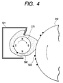
- a dielectric brush is formed from ferrite carrier 502 as low resistance carrier contained in a container (not shown), by which the surface of the photosensitive drum 342 is uniformly charged, thereby preparing for formation of the latent image.
- the latent image is formed on the surface of the photosensitive drum 342 by light from the LED array 210 and then is developed by the developing device 322 to form a toner image.
- development is effected by applying developing bias between the photosensitive drum 342 and the developing sleeve 354.
- a transfer charger 323 urged against the photosensitive drum 342 with the interposition of a transfer belt 333 as transfer means below the developing device 322 effects discharging from the back side of the transfer belt 333, with the result that the toner image on the photosensitive drum 342 is transferred onto a recording paper on the transfer belt 333.
- toner 503 remaining on the photosensitive drum 342 is once received by the charger 321 to change the electrostatic property of the photosensitive drum. Thereafter, the toner is returned to the photosensitive drum 342 again and then is collected by the developing device 322.
- Recording papers contained in a cassette 340 or 341 are fed one by one onto the moving transfer belt 333 by a pick-up roller 338 or 339 and sheet feeding rollers 336, 337.
- the transfer belt 333 is shifted by a transfer belt roller 348 disposed below the Y image forming portion 317, M image forming portion 318, C image forming portion 319 and K image forming portion 320.
- a leading end of the recording paper fed to the transfer belt 333 is detected by a sheet leading end sensor 347.
- a detection signal from the sheet leading end sensor is sent from the color printer portion 2 to the color reader portion 1 and is used as a sub-scanning synchronous signal when the video signal is sent from the color reader portion 1 to the color printer portion 2.
- the recording paper is conveyed by the transfer belt 333, and the toner images are successively formed on the recording paper in the image forming portions 317 to 320 in the order of Y, M, C and K.
- the recording paper After the recording paper is passed through the K image forming portion 320, electricity is removed from the recording paper by an electricity removing charger 349 in order to facilitate the separation of the recording paper from the transfer belt 333. Then, the recording paper is separated from the transfer belt 333.
- a peeling charger 350 disposed adjacent to the electricity removing charger 349 prevent distortion of the image due to peel discharging generated when the recording paper is separated from the transfer belt 333.
- the separated recording paper is charged by a pre-fixing chargers 351 and 352 to promote a toner attracting force thereby to prevent the image distortion. Thereafter, the toner images are thermally fixed to the recording paper by a fixing device 334. Then, the recording paper is discharged onto a sheet discharge tray 335. Further, electricity is removed from the transfer belt 333 by inner and outer electricity removing chargers 353.
- the signals from the image processing portion are binalized in the binary converting portion 201 and then are sent to video signal counting portions 220 to 223 as image information detecting means.
- the video signal counting portions 220 to 223 the total numbers of the LEDs being illuminated are counted for the respective color images.
- the binalized image signals are inputted to delay portions 202, 203, 204 and 205 where the signals are delayed in accordance with respective image forming positions and the sheet leading end sensor 347, respectively. Then, the signals are sent to LED drivers 206, 207, 208 and 209.
- the LED driving portion 206, 207, 208 and 209 serve to form or generate signals for driving LED portions 210, 211, 212 and 213.
- the return bias applying time period is determined in accordance with an endurance level value sought from an image density total value from the initial condition of the image bearing member and from a count total value, and an image density total value between predetermined number count values obtained by number measuring means (not shown).
- the image density is detected.
- the image density for each color image the total number of illuminated LEDs counted in the video count portion 220, 221, 222 or 223 as video counting means shown in Fig. 3.
- Fig. 5 shows the video signal count portion 220 in detail.
- the video signal count portions 221 to 223 have the same constructions as that of the video signal count portion 220.
- the image signal 700 sent from the binary converting portion 201 is counted by 29-bit counters 701 to 708 in parallel for each 8-bit as an image signal for one image, and counted results are added to each other by a 32-bit adder 709, thereby obtaining the total number of illuminated LEDs as 32-bit data.
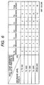
- Such processing is effected for each image formation to seek the total number of illuminated LEDs (referred to as "video count” hereinafter), and a value obtained by successively adding the total numbers from the initial condition of the photosensitive drum 342 upon installation of the apparatus is regarded as V sum . Further, a value (calculated in terms of A4 sheet size) obtained by successively adding the image formation numbers from the initial condition of the photosensitive drum 342 upon installation of the apparatus is regarded as N sum .
- a time period T2 for removing the residual toner is set to 60 seconds.
- T T1 + T2.
- DC of -700 V and AC bias having a rectangular wave of 1.1 kV pp , 1 kHz and 50% duty are applied to the charger associated with the rotating photosensitive drum and the developing sleeve is driven, and DC of -550 V and AC bias having a rectangular wave of 1 kV pp , 2.2 kHz and 60% duty are applied to the developing device and the developing sleeve is driven.
- the charger once receives the toner on the photosensitive drum to change the electrostatic property and then returns the toner to the photosensitive drum again, and, thereafter, the developing device collects the toner.
- the video count total value V 25 for previous 25 sheets and the image formation number count value for seeking the value T2 are reset.
- a step S5 the feeding of the sheet waiting at the registration roller position is started and the image formation is effected.
- the residual toner may be transferred to the transfer belt and then may be collected by a transfer belt cleaner.
- a potential sensor may be provided around the photosensitive drum to measure the potential of the photosensitive drum.
- the transfer-residual toner on the latent image bearing member can be removed by the action of the charging means
- the transfer-residual developer on the latent image bearing member can be removed and collected without worsening the charging ability of the charging means.
- the present invention provides an image forming apparatus which has an image bearing member, charging device for charging the image bearing member, electrostatic image forming device for selectively removing charges on the image bearing member charged by the charging device to form an electrostatic image, developing means for developing the electrostatic image with toner as a toner image, transfer device for transferring the toner image on the image bearing member onto a transfer material, the charging device temporarily collecting residual toner after the transferring, return bias applying device for applying a return bias for returning the toner collected in the charging device to the image bearing member in a non-image forming period, and control means for controlling a length of a length of a return bias applying time period of the return bias applying device.
Landscapes
- Physics & Mathematics (AREA)
- General Physics & Mathematics (AREA)
- Engineering & Computer Science (AREA)
- Plasma & Fusion (AREA)
- Control Or Security For Electrophotography (AREA)
- Cleaning In Electrography (AREA)
- Electrostatic Charge, Transfer And Separation In Electrography (AREA)
- Color Electrophotography (AREA)
Abstract
Description
Claims (5)
- An image forming apparatus comprising:an image bearing member;charging means for charging said image bearing member;electrostatic image forming means for selectively removing charges on said image bearing member charged by said charging means to form an electrostatic image;developing means for developing the electrostatic image with toner as a toner image;transfer means for transferring the toner image on said image bearing member onto a transfer material;said charging means temporarily collecting residual toner after the transferring;return bias applying means for applying a return bias for returning the toner collected in said charging means to said image bearing member in a non-image forming period; andcontrol means for controlling a length of a return bias applying time period of said return bias applying means.
- An image forming apparatus according to claim 1, wherein said developing means collects the toner returned from said charging means to said image bearing member.
- An image forming apparatus according to claim 1, wherein said control means controls the length of the return bias applying time period on the basis of an image information amount and an image formation number.
- An image forming apparatus according to claim 1, wherein said charging means has a particle layer slidingly contacted with said image bearing member, and the residual toner on said image bearing member is collected within said particle layer.
- An image forming apparatus according to claim 1, wherein said transfer means have an intermediate transfer member for once bearing the toner image on said image bearing member and then transferring the toner image onto the transfer material, and cleaning means for cleaning said intermediate transfer member, and the toner returned from said charging means to said image bearing member is transferred to said intermediate transfer member and then is cleaned by said cleaning means.
Applications Claiming Priority (2)
| Application Number | Priority Date | Filing Date | Title |
|---|---|---|---|
| JP30124799 | 1999-10-22 | ||
| JP30124799A JP3408214B2 (en) | 1999-10-22 | 1999-10-22 | Image forming device |
Publications (3)
| Publication Number | Publication Date |
|---|---|
| EP1094369A2 true EP1094369A2 (en) | 2001-04-25 |
| EP1094369A3 EP1094369A3 (en) | 2002-05-15 |
| EP1094369B1 EP1094369B1 (en) | 2006-08-23 |
Family
ID=17894550
Family Applications (1)
| Application Number | Title | Priority Date | Filing Date |
|---|---|---|---|
| EP00122868A Expired - Lifetime EP1094369B1 (en) | 1999-10-22 | 2000-10-20 | Image forming apparatus |
Country Status (4)
| Country | Link |
|---|---|
| US (1) | US6529698B1 (en) |
| EP (1) | EP1094369B1 (en) |
| JP (1) | JP3408214B2 (en) |
| DE (1) | DE60030228T2 (en) |
Families Citing this family (1)
| Publication number | Priority date | Publication date | Assignee | Title |
|---|---|---|---|---|
| JP4908835B2 (en) * | 2005-12-05 | 2012-04-04 | キヤノン株式会社 | Image forming apparatus |
Family Cites Families (11)
| Publication number | Priority date | Publication date | Assignee | Title |
|---|---|---|---|---|
| JP2880356B2 (en) | 1991-10-30 | 1999-04-05 | 沖電気工業株式会社 | Image forming apparatus and image forming method |
| US5765076A (en) * | 1995-05-26 | 1998-06-09 | Oki Data Corporation | Method and apparatus for forming an electrostatic latent image with toner recovery |
| JP3453473B2 (en) | 1995-05-30 | 2003-10-06 | キヤノン株式会社 | Foamed conductive roller, method of manufacturing the same, and electrophotographic apparatus using the same |
| DE69638350D1 (en) * | 1995-09-28 | 2011-05-19 | Canon Kk | Image forming apparatus |
| JPH10228160A (en) * | 1996-12-13 | 1998-08-25 | Canon Inc | Image forming device |
| JPH10198126A (en) | 1996-12-29 | 1998-07-31 | Minolta Co Ltd | Charging device |
| JPH10221932A (en) | 1997-02-04 | 1998-08-21 | Minolta Co Ltd | Electrifier |
| US5999773A (en) * | 1997-06-12 | 1999-12-07 | Ricoh Company, Ltd. | Image forming apparatus and cleaning method for contact-charging member |
| JP3576761B2 (en) | 1997-07-31 | 2004-10-13 | キヤノン株式会社 | Image forming device |
| US6215967B1 (en) * | 1997-12-25 | 2001-04-10 | Canon Kabushiki Kaisha | Image forming apparatus with a controlled cleaning operation feature |
| US6002907A (en) * | 1998-12-14 | 1999-12-14 | Xerox Corporation | Liquid immersion development machine having a reliable non-sliding transfusing assembly |
-
1999
- 1999-10-22 JP JP30124799A patent/JP3408214B2/en not_active Expired - Fee Related
-
2000
- 2000-10-19 US US09/691,170 patent/US6529698B1/en not_active Expired - Fee Related
- 2000-10-20 DE DE60030228T patent/DE60030228T2/en not_active Expired - Lifetime
- 2000-10-20 EP EP00122868A patent/EP1094369B1/en not_active Expired - Lifetime
Also Published As
| Publication number | Publication date |
|---|---|
| DE60030228D1 (en) | 2006-10-05 |
| DE60030228T2 (en) | 2007-08-09 |
| EP1094369B1 (en) | 2006-08-23 |
| EP1094369A3 (en) | 2002-05-15 |
| JP3408214B2 (en) | 2003-05-19 |
| JP2001117449A (en) | 2001-04-27 |
| US6529698B1 (en) | 2003-03-04 |
Similar Documents
| Publication | Publication Date | Title |
|---|---|---|
| JP4798854B2 (en) | Image forming apparatus and residual toner removing method in image forming apparatus | |
| US6529698B1 (en) | Image forming apparatus featuring a variable toner return bias applying time | |
| US7209159B2 (en) | Image forming apparatus and image forming control method | |
| EP0992865B1 (en) | Image formation apparatus and control method thereof | |
| JP3618992B2 (en) | Image forming apparatus | |
| JP2003162109A (en) | Color image forming equipment | |
| US6947680B2 (en) | Image forming apparatus | |
| JP4040346B2 (en) | Image forming apparatus | |
| JP3897464B2 (en) | Image forming apparatus | |
| JP2011049969A (en) | Image reading apparatus | |
| JP3884871B2 (en) | Image forming apparatus and method of controlling image forming apparatus | |
| JP3402980B2 (en) | Image forming device | |
| US6343202B1 (en) | Image forming apparatus for correcting image formation timing of plural image forming units | |
| JP2001337504A (en) | Image forming device | |
| JP2005215281A (en) | Residual toner recovery method and image forming apparatus | |
| JP3997048B2 (en) | Image forming apparatus | |
| JP2003162182A (en) | Image forming device | |
| JP3403013B2 (en) | Image forming device | |
| JPH09190079A (en) | Image forming device | |
| JPH11163885A (en) | Serial load controller | |
| JPH11212415A (en) | Image forming device | |
| JP2004315183A (en) | Recording medium identification device | |
| JP2004315185A (en) | Recording medium identification device | |
| JP2001119971A (en) | Vibration wave motor drive control device and drive control method | |
| JP2000250281A (en) | Multicolor image forming device |
Legal Events
| Date | Code | Title | Description |
|---|---|---|---|
| PUAI | Public reference made under article 153(3) epc to a published international application that has entered the european phase |
Free format text: ORIGINAL CODE: 0009012 |
|
| AK | Designated contracting states |
Kind code of ref document: A2 Designated state(s): AT BE CH CY DE DK ES FI FR GB GR IE IT LI LU MC NL PT SE |
|
| AX | Request for extension of the european patent |
Free format text: AL;LT;LV;MK;RO;SI |
|
| PUAL | Search report despatched |
Free format text: ORIGINAL CODE: 0009013 |
|
| AK | Designated contracting states |
Kind code of ref document: A3 Designated state(s): AT BE CH CY DE DK ES FI FR GB GR IE IT LI LU MC NL PT SE |
|
| AX | Request for extension of the european patent |
Free format text: AL;LT;LV;MK;RO;SI |
|
| 17P | Request for examination filed |
Effective date: 20020927 |
|
| AKX | Designation fees paid |
Designated state(s): DE FR GB IT |
|
| 17Q | First examination report despatched |
Effective date: 20031219 |
|
| GRAP | Despatch of communication of intention to grant a patent |
Free format text: ORIGINAL CODE: EPIDOSNIGR1 |
|
| GRAS | Grant fee paid |
Free format text: ORIGINAL CODE: EPIDOSNIGR3 |
|
| GRAA | (expected) grant |
Free format text: ORIGINAL CODE: 0009210 |
|
| AK | Designated contracting states |
Kind code of ref document: B1 Designated state(s): DE FR GB IT |
|
| PG25 | Lapsed in a contracting state [announced via postgrant information from national office to epo] |
Ref country code: IT Free format text: LAPSE BECAUSE OF FAILURE TO SUBMIT A TRANSLATION OF THE DESCRIPTION OR TO PAY THE FEE WITHIN THE PRESCRIBED TIME-LIMIT;WARNING: LAPSES OF ITALIAN PATENTS WITH EFFECTIVE DATE BEFORE 2007 MAY HAVE OCCURRED AT ANY TIME BEFORE 2007. THE CORRECT EFFECTIVE DATE MAY BE DIFFERENT FROM THE ONE RECORDED. Effective date: 20060823 |
|
| REG | Reference to a national code |
Ref country code: GB Ref legal event code: FG4D |
|
| REF | Corresponds to: |
Ref document number: 60030228 Country of ref document: DE Date of ref document: 20061005 Kind code of ref document: P |
|
| ET | Fr: translation filed | ||
| PLBE | No opposition filed within time limit |
Free format text: ORIGINAL CODE: 0009261 |
|
| STAA | Information on the status of an ep patent application or granted ep patent |
Free format text: STATUS: NO OPPOSITION FILED WITHIN TIME LIMIT |
|
| 26N | No opposition filed |
Effective date: 20070524 |
|
| PGFP | Annual fee paid to national office [announced via postgrant information from national office to epo] |
Ref country code: FR Payment date: 20091030 Year of fee payment: 10 Ref country code: IT Payment date: 20091015 Year of fee payment: 10 |
|
| PG25 | Lapsed in a contracting state [announced via postgrant information from national office to epo] |
Ref country code: FR Free format text: LAPSE BECAUSE OF NON-PAYMENT OF DUE FEES Effective date: 20101102 |
|
| REG | Reference to a national code |
Ref country code: FR Ref legal event code: ST Effective date: 20110630 |
|
| PG25 | Lapsed in a contracting state [announced via postgrant information from national office to epo] |
Ref country code: IT Free format text: LAPSE BECAUSE OF NON-PAYMENT OF DUE FEES Effective date: 20101020 |
|
| PGFP | Annual fee paid to national office [announced via postgrant information from national office to epo] |
Ref country code: DE Payment date: 20131031 Year of fee payment: 14 Ref country code: GB Payment date: 20131018 Year of fee payment: 14 |
|
| REG | Reference to a national code |
Ref country code: DE Ref legal event code: R119 Ref document number: 60030228 Country of ref document: DE |
|
| GBPC | Gb: european patent ceased through non-payment of renewal fee |
Effective date: 20141020 |
|
| PG25 | Lapsed in a contracting state [announced via postgrant information from national office to epo] |
Ref country code: DE Free format text: LAPSE BECAUSE OF NON-PAYMENT OF DUE FEES Effective date: 20150501 Ref country code: GB Free format text: LAPSE BECAUSE OF NON-PAYMENT OF DUE FEES Effective date: 20141020 |