EP1093925A2 - Head drive circuit for impact dot printer - Google Patents
Head drive circuit for impact dot printer Download PDFInfo
- Publication number
- EP1093925A2 EP1093925A2 EP00309276A EP00309276A EP1093925A2 EP 1093925 A2 EP1093925 A2 EP 1093925A2 EP 00309276 A EP00309276 A EP 00309276A EP 00309276 A EP00309276 A EP 00309276A EP 1093925 A2 EP1093925 A2 EP 1093925A2
- Authority
- EP
- European Patent Office
- Prior art keywords
- voltage
- head
- input
- coil
- power source
- Prior art date
- Legal status (The legal status is an assumption and is not a legal conclusion. Google has not performed a legal analysis and makes no representation as to the accuracy of the status listed.)
- Granted
Links
Images




Classifications
-
- B—PERFORMING OPERATIONS; TRANSPORTING
- B41—PRINTING; LINING MACHINES; TYPEWRITERS; STAMPS
- B41J—TYPEWRITERS; SELECTIVE PRINTING MECHANISMS, i.e. MECHANISMS PRINTING OTHERWISE THAN FROM A FORME; CORRECTION OF TYPOGRAPHICAL ERRORS
- B41J2/00—Typewriters or selective printing mechanisms characterised by the printing or marking process for which they are designed
- B41J2/22—Typewriters or selective printing mechanisms characterised by the printing or marking process for which they are designed characterised by selective application of impact or pressure on a printing material or impression-transfer material
- B41J2/23—Typewriters or selective printing mechanisms characterised by the printing or marking process for which they are designed characterised by selective application of impact or pressure on a printing material or impression-transfer material using print wires
- B41J2/30—Control circuits for actuators
Definitions
- the present invention relates to an impact dot printer, and more specifically, relates to a circuit for driving a head of an impact dot printer and to a power control technique for controlling a power source for a head drive circuit.
- an impact dot printer drives a print wire by using, for example, the magnetic attractive force of an electromagnet.
- Fig. 8 is a diagram showing an example wire impact print head for the print head of the thus arranged impact dot printer.
- a wire impact print head 51 has a plurality of wires 57 that are attached, by wire levers 53 and return springs 55, so that they reciprocate.
- a drive current flows through a head coil 59
- a wire lever 53 is attracted by the magnetic attractive force produced by the electromagnet in the direction indicated by an arrow in Fig. 8, and a wire 57 strikes an ink ribbon 61 and forms dots on a printing sheet 65 moved in consonance with the rotation of a platen 63.
- Fig. 9 is a diagram illustrating the fundamental structure of the circuit of the print head 51 for driving the head coil 59.
- a drive circuit (driver) 30 for each head coil 59 is constituted by one of the head drive transistors 33, a head drive power source 34 and a Zener diode 35.
- a control pulse 32 is maintained at level H by a print controller 31, and a pertinent head drive transistor 33 is maintained in the ON state (in the saturated region).
- a voltage (e.g., 35V) supplied by the head drive power source 34 is applied to the head coil 59, and a drive current i1 flows through it.
- the control pulse 32 falls to level L
- the head coil 59 generates an inductive electromotive force to render off the head drive transistor 33.
- the Zener diode 35 is rendered conductive at the induced voltage, and a base current flows to the head drive transistor 33, while the head drive transistor 33 enters a linear operating region.
- the drive current i1 flows through the head drive transistor 33 and the current value is drastically reduced, and as a result, the head drive transistor 33 is rendered off.
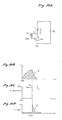
- FIG. 10A to 10D In these drawings are presented a diagram showing a simplified head drive circuit, and other diagrams showing the flow of the drive current, as well as its current waveform and the operation of the Zener diode.
- a drive current i is supplied by a power source Vp in the direction indicated by the arrow, and a head coil is driven.
- V CE collector-emitter voltage
- the Zener diode is rendered conductive, and a base current flows via the Zener diode to the transistor, as is indicated by a broken line in Fig. 10A. Then, the charge on the transistor falls in the linear operation mode, and the energy accumulated in the coil is discharged through the collector and the emitter of the transistor. When the discharge of the energy has been completed, the Zener diode is again rendered non-conductive and the transistor is rendered off.
- Figs. 10B and 10C are graphs showing the changes produced by this process in the collector current i and the collector-emitter voltage (V CE ) of the transistor as time elapses.
- V CE collector-emitter voltage
- the power supplied by the power source to render off the transistor is lost and is not effectively employed. Furthermore, since a great deal of heat is generated by the transistor, a cooling member, such as a heat sink, is also required, and accordingly, the size of the package of a power source is enlarged.
- a head drive circuit for an impact dot printer which performs printing by driving a print wire, comprising:
- the head drive circuit is so configured that the voltage regulator returns to the power source the power that accumulates when the switching element (e.g., a transistor) is rendered off.
- the switching element e.g., a transistor
- the energy that accumulates in the head coil when the switching element is turned off is returned to the power source by the voltage regulator, and is effectively utilized for driving the head coil.
- a DC/DC converter or a voltage dropper may be adopted as the voltage regulator.
- the voltage introducer includes a first rectifier which is rendered conductive when the inductive voltage is generated in the head coil to unidirectionally supply the inductive voltage into the voltage regulator as the input voltage, and the voltage returner includes a second rectifier for unidirectionally supplying the output voltage from the voltage regulator to the DC power source.
- diodes may be adopted as the rectifiers.
- the rectifiers e.g., diodes
- the backflow of power, from the input end of the voltage regulator to the switching element, or the inverted supply of power, from the power source to the output end of the voltage regulator can be prevented.
- the head drive circuit further comprises an input voltage adjuster for adjusting the input voltage of the voltage regulator so as to have a predetermined value higher than the power source voltage.
- an input voltage adjuster for adjusting the input voltage of the voltage regulator so as to have a predetermined value higher than the power source voltage. Specifically, so long as the input voltage of the voltage regulator is raised to a predetermined voltage that only when the switching element is rendered off is higher than the voltage provided by the power source, the power from the head coil can be led to the voltage regulator and can thereafter be returned to the power source by a high induction voltage that is generated at the head coil.
- the voltage regulator includes an input condenser for smoothing the input voltage thereof.
- the voltage adjuster includes a charger for charging the input condenser so as to have the predetermined value of input voltage before and while the printing is performed.
- the charger always applies the predetermined value of voltage to the input condenser.
- the switching element is turned on/off repeatedly at a frequency too high to drive the print wire to apply the inductive voltage to the input condenser repeatedly at least before the printing is performed, thereby the switching element and the head coil serve as the charger.
- the charging operation using the switching element and the head coil may be used not only for the initial charging performed before the printing is started, but may also be used, as needed, during the printing operation (e.g., following a line return) to supplement the discharging of the condenser.
- the charger includes: a charge coil; a coil switching element which is on/off controlled to apply the power source voltage to the charge coil; and an input voltage holder for inputting an inductive voltage, generated in the charge coil when the coil switching element is turned off, to the input condenser.
- the coil switching element is turned on/off repeatedly to apply the inductive voltage generated in the charge coil to the input condenser repeatedly at least while the printing is performed, thereby the charged voltage in the input condenser is maintained at the predetermined value.
- the input voltage holder may be employed not only for supplementary charging during the printing, but also for the initial charging performed before printing is begun.
- FIG. 1 is a diagram showing the arrangement of a head drive circuit according to a first embodiment of the present invention.
- the head drive circuit comprises: a head drive transistor 33, for driving a head coil 59; a constant voltage-input DC/DC converter 2, which has an input voltage of 90V and an output voltage of 35V that is equivalent to that of a head drive power source 34; an initial voltage charger 4, for raising the voltage input by the constant voltage-input DC/DC converter 2 to 90V; a diode 6 (a first rectifier) the anode of which is connected to the head coil 59 and a collector 10 of the head drive transistor 33 and the cathode of which is connected to the input end of the constant voltage-input DC/DC converter 2; and a diode 8 (a second rectifier) the anode of which is connected to the output end of the constant input DC/DC converter 2 and the cathode of which is connected to the head drive power source 34.
- a diode 6 a first rectifier
- the anode of which is connected to the head coil 59 and a collector 10 of the head drive transistor 33 and the cathode of which is
- a related Zener diode which connects the head coil 59 and the base of the head drive transistor 33, is not provided for the head drive circuit of this embodiment. And the operation of the constant voltage-input DC/DC converter 2 is so controlled that the input voltage is 90V and the output voltage is equal to a voltage, such as 35V, obtained by adding the voltage drop at the diode 8 of the head drive power source 34.
- the initial voltage charger 4 sets a voltage of 90V as the input voltage for the constant voltage-input DC/DC converter 2 (the charge voltage for a smoothing condenser 2a in Fig. 2, which will be described later, that is provided at the input end of the DC/DC converter 2).
- the head drive transistor 33 When the head drive transistor 33 is rendered on, a drive current supplied by the head drive power source 34 drives the head coil 59.
- the head drive transistor 33 is rendered off, an induced electromotive force is generated at the head coil 59, so that a high voltage is produced at the collector 10 of the head drive transistor 33 and is clamped at the 90V input voltage of the DC/DC converter 2.
- the drive current i is absorbed by the constant voltage-input DC/DC converter 2, is returned, via the diode 8, from the output end of the DC/DC converter 2 to the head drive power source 34, and is employed again.
- Fig. 2 is a circuit diagram showing the constant voltage-input DC/DC converter 2 and the initial voltage charger 4.
- the constant voltage-input DC/DC converter 2 employs a drive controller 2d to switch a chopper transistor 2b in order to control a duty ratio. Therefore, the 90V input voltage of the DC/DC converter 2 is chopped, and on the output side, the obtained voltage waveform is smoothed and reduced by a condenser 2c to provide a constant 35V output, while a feedback diode 2e feeds the energy accumulated at a DC reactor 2f back to the condenser 2c when the transistor 2b is rendered off.
- a transformer 4a reduces an AC voltage of 100V, received from a commercially available power source, to an AC voltage of 90V.
- the AC voltage of 90V is rectified by a diode 4b, and the obtained voltage is smoothed by a condenser 4c to provide a DC voltage of 90V that is applied to the input end of the constant voltage-input DC/DC converter 2.
- a condenser 4c smoothed by a condenser 4c to provide a DC voltage of 90V that is applied to the input end of the constant voltage-input DC/DC converter 2.
- a constant voltage-input of 90V is maintained for the input voltage DC/DC converter 2.
- the initial voltage charger 4 is not limited to the arrangement shown in Fig. 2.
- Figs. 3A to 3D are diagrams showing a simplified circuit for the head drive circuit according to this embodiment, and graphs showing the flow of a drive current and its current waveform. The operation of the head drive circuit of this embodiment will now be explained while referring to Figs. 3A to 3D.
- the absorbed current is thereafter transformed by the constant voltage-input DC/DC converter 2 to provide a DC current having substantially the same voltage as the voltage Vp provided by the head drive power source 34, and the obtained DC current is transmitted, via the diode 8, from the output end of the DC/DC converter 2 to the head drive power source 34. Therefore, since the head drive transistor 33 can be immediately and completely rendered off, and since the current that flows through the head drive transistor 33 is substantially zero, as is shown in Fig. 3D there is no substantial power loss at the head drive transistor 33. That is, as is indicated by the right-down hatching in Fig.
- the power P1 that is to be wasted in the related circuit when the head drive transistor 33 is rendered off can be returned to the power source 34 and employed again as head driving energy.
- the heat generated by the transistor 33 is also reduced considerably, so that only a simple cooling countermeasure is required and the size of a power source package can be reduced.
- the head coil and the drive transistor are constituted at one stage.
- the arrangement, however, is not limited to this one, and drive transistors may, for example, be provided in both the upper and lower stages and employed for the respective upper and lower head coils.
- the waveform of the drive current would differ from that shown in Fig. 3B; however, also in such a configuration, the energy wasted when the transistor is in the OFF state can be returned to the head drive power source and employed again.
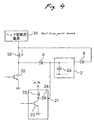
- Fig. 4 is a diagram showing the arrangement of a head drive circuit according to a second embodiment of the present invention.
- the head drive circuit differs from the circuit for the first embodiment in Fig. 1, in that the initial voltage charger 4 is replaced with an input voltage holder 21.
- a charge coil 22, a child drive transistor 23 and a diode 24 are connected in the same manner as are a head coil 59, a head drive transistor 33 and a diode 6 that together constitute the print wire drive circuit; however, the current capacity is smaller than that of the print wire drive circuit.
- the head coil 59 and the head drive transistor 33, which constitute the print wire drive circuit, are repetitiously and rapidly driven at short intervals, so that an initial charge is placed on a condenser 2a (hereinafter referred to simply as a condenser 2a) on the input side of the constant voltage-input DC/DC converter 2.
- the input voltage holder 21 is driven as needed to place supplemental charges on the condenser 2a, so that a reduction in the input voltage due to the discharging of the condenser 2a can be prevented.
- the initial charging is performed, at a predetermined time, for the constant voltage-input DC/DC converter 2.
- the print wire in the head is repeatedly and rapidly driven by pulses, emitted by the print wire drive circuit, that are short enough to prevent the print wire from actually being operated. That is, ON/OFF pulses emitted at such a high frequency that they do not drive the print wire are transmitted to the base-emitter of the head drive transistor 33.
- the head drive transistor 33 is repetitively and rapidly rendered on and off, while the head coil 59 accumulates from the power source 34 energy that is transmitted to and is used to place a charge on the condenser 2a of the DC/DC converter 2. This process is repeated until the condenser 2a is charged to 90V. Thereafter, the normal printing operation is begun.
- the input voltage holder 21 Since the charge voltage on the condenser 2a gradually drops during printing, periodically, or as needed, e.g., each time the printing of one line is completed or each time a string of 40 characters has been printed, at the same high pulse as is employed for the initial charging, the input voltage holder 21 is rapidly and repetitiously turned on and off during a specific period. In this manner, supplemental charging of the condenser 2a is performed, and the charge voltage held by the condenser 2a is maintained substantially at the 90V level.
- the input voltage holder 21 includes: the charge coil 22; the coil drive transistor 23, which drives the charge coil 22; and a diode 24, which is rendered conductive by the inductive electromotive force that is generated at the charge coil 22 when the coil drive transistor 23 is turned off and which transmits a current to the input end of the DC/DC converter 2.
- the supplemental charging process for the input voltage holder 21 is exactly the same as the initial charging process performed for the print wire drive circuit. That is, each time the transistor 23 is rendered on, energy is accumulated by the charging coil 22, and each time the transistor 23 is rendered off, the accumulated energy is transmitted, via the diode 24, to the condenser 2a.
- the voltage held by the condenser 2a is supplemented, and is maintained at the 90V level.
- the charge current used for the supplemental charging may be smaller than the charge current that is required for the initial charging, so that the current capacity of the input voltage holder 21 may be smaller than that of the print wire drive circuit.
- Figs. 5A and 5B are diagrams showing the waveform of the print wire drive circuit during printing.
- the waveform of the current that flows through the head coil 59 is shown in Fig. 5A
- the waveform of the collector-emitter voltage of the head drive transistor 33 is shown in Fig. 5B
- Figs. 5C and 5D are diagrams showing the waveforms of the print wire drive circuit during the initial charging.
- the waveform of the initial charge current that flows through the head coil 59 is shown in Fig. 5C
- the waveform of the base-emitter voltage at the head drive transistor 33 is shown in Fig. 5D.
- the head drive transistor 33 is driven by a pulse having a frequency of substantially 1 to 2kHz, as is shown in Fig. 5B. Then, the current shown in Fig. 5A flows to the head coil 59 and the print wire is driven.
- the head drive transistor 33 is repetitively, about 1000 times, rendered on and off, for about 100ms, using a pulse having a frequency of about 10kHz, as shown in Fig. 5D (e.g., an ON time width of 20 ⁇ s and an OFF time width of 80 ⁇ s). As a result, a tiny pulse current having the short time width shown in Fig.
- the current in the portions wherein the head drive transistor 33 has been rendered off flows, via the diode 24, as a charge current to the condenser 2a of the constant voltage-input DC/DC converter 2.
- the charge current is repetitively supplied 1000 times, the charge voltage held by the condenser 2a is increased until it is substantially 90V.
- the supplemental charging which is performed during the printing process by the input voltage holder 21, can be effected by rendering on and off the coil drive transistor 23 at a pulse having the same frequency as that employed for the initial charging, or at a pulse having a higher frequency.
- a charge inductance 22 of 3300 ⁇ H is employed to drive the coil drive transistor 23 following each line return at a pulse having a frequency of 25kHz and an ON time of 3 ⁇ s.
- the input voltage holder 21 since the input voltage holder 21 only performs supplemental charging, its current capacity is smaller than that of the wire drive circuit. As a modification, the current capacity of the input voltage holder 21 may be increased to that of the print wire drive circuit, so that the input voltage holder 21 can also perform the pre-printing initial charging. Or instead, the printing wire drive circuit and the input voltage holder 21 may together be employed to perform the initial charging.
- the supplemental charging may be performed by the print wire drive circuit, without the input voltage holder 21 being provided.
- the print wire drive circuit For the supplemental charging, for example, following each line return the print wire drive circuit need only be driven at a pulse having as high a frequency as the one used for the initial charging (only a few driving operations are required, compared with the number that is needed for the initial charging).
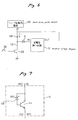
- Fig. 6 is a diagram showing the arrangement of a head drive circuit according to a third embodiment of the present invention.
- the head drive circuit differs from the circuit for the first embodiment shown in Fig. 6, in that the constant voltage-input DC/DC converter 2 and the initial voltage charger 4 are replaced with a constant voltage dropper 12.
- the head driving circuit comprises: a head driver transistor 33, for driving a head coil 59; a constant voltage dropper 12, which reduces, to a predetermined voltage value, an induction voltage that is generated at the head coil 59 when the head driver transistor 33 is turned off and which returns the obtained voltage to a head driving power source 34; and a diode 6, the anode of which is connected to the head coil 59 and a collector 10 of the head driver transistor 33 and the cathode of which is connected to the input end of the constant voltage dropper 12.
- the constant voltage dropper 12 is constituted by a transistor 2a and a Zener diode 2b.
- the collector of the transistor 2a is connected to the cathode of the Zener diode 2b
- the base of the transistor 2a is connected to the anode of the Zener diode 2b
- the emitter (the output end of the constant voltage dropper 12) of the transistor 2a is connected to the head driving power source 34.
- the Zener voltage of the Zener diode 2b is 55V
- the voltage of the head driving power source 34 is 35V. That is, the constant voltage dropper 12 is so designed that a current flows through it when the input voltage is 90V.
- the head driver transistor 33 When the head driver transistor 33 is turned off, the induced electromotive force having the polarities shown in Fig. 3A is generated at the head coil 59, and a high induction voltage is produced.
- the induction voltage is 90V
- the drive current i flows via the diode 6 to the constant voltage dropper 12, as indicated by an arrow in Fig. 3A.
- the power absorbed by the constant voltage dropper 12 is returned, via the Zener diode 2b (for which the Zener voltage is 55V), from the output end of the constant voltage dropper 12 to the head driving power source 34.
- the head driver transistor 33 when the head driver transistor 33 is turned on, the drive current i flows from the head driving power source 34, and the power P shown in Fig. 3B is supplied to and drives the head coil 59. Then, when the head driver transistor 33 is turned off, an induced electromotive force having the polarities shown in Fig. 3A is produced at the head coil 59, the collector voltage of the head transistor 33 is raised as is shown in Fig. 3C, and power P1 (right-down hatched portion in Fig. 3B) is supplied from the head coil 59 to the constant voltage dropper 12. The power that is obtained by subtracting, from the power P1, the power that is consumed by the constant voltage drop circuit 55 to reduce the voltage 55V is returned to the head driving power source 34.
- the head driver transistor 33 can be immediately and completely rendered off, and since the current that flows through the head driver transistor 33 is substantially zero, there is no substantial power loss at the head driver transistor 33, as is shown in Fig. 3D. That is, as is indicated in the right-down hatched portion in Fig. 3B, in this embodiment the power P1 that is to be wasted in the related art, when the head driver transistor 33 is rendered off, can be returned to the power source 34, and can be used again as head driving energy. The heat generated by the transistor 33 is also considerably reduced, so that only a simple cooling countermeasure is required, and the size of the package of a power source can be reduced.
- the ratio of the power P1 (the right-down hatched portion in Fig. 3B) in the OFF state to the total power P (the left-down hatched portion in Fig. 3B) that flows through the head coil 59, i.e., P1/P, is normally 0.15 to 0.20 (15 to 20%).
- the ratio of the power consumed by the constant voltage dropper 12 to the power P1 when the head transistor 33 is turned off is (55V/90V) x 100 ⁇ 60%. Therefore, when the head transistor 33 is turned off approximately 40% of the power P1 is returned to the head driving power source 34 and is effectively utilized.
- the increased power efficiency that the constant voltage dropper 12 makes available can be obtained as follows.
- the power efficiency is 0.15 x (35/90) x 100 ⁇ 6%, and the power efficiency, in other words, can be increased about 6%.
- the power that is accumulated at the head coil 59 when the head driver transistor 33 is turned on is partially consumed by the constant voltage dropper 12 when the transistor 33 is turned off, and the remaining power is returned to the head driving power source 34. Therefore, since the power accumulated at the head coil 59 is not lost due to heat generation at the head driver transistor 33, a part of this power can be effectively used again as energy for driving the head coil. Thus, the efficiency of the head driving power source can be improved.
- the head driver transistor 33 since heat generated by the head driver transistor 33 is also drastically reduced by this method, only a simple heat sink is required for the transistor 33, and the power source package can be compactly made. Furthermore, since the consumption of power by the head driver transistor 33 can also be reduced, the head can be efficiently driven, and as a result, the entire power supply apparatus can be made compactly.
Landscapes
- Dot-Matrix Printers And Others (AREA)
- Printers Or Recording Devices Using Electromagnetic And Radiation Means (AREA)
Abstract
Description
Claims (10)
- A head drive circuit for an impact dot printer which performs printing by driving a print wire, comprising:a DC power source for supplying a power source voltage;a head coil;a switching element which is on/off controlled to apply the power source voltage to the head coil for a predetermined time period;a voltage regulator for converting an input voltage having a value higher than the power source voltage into an output voltage having a value as substantially same as the power source voltage;a voltage introducer for inputting an inductive voltage, generated in the head coil when the switching element is turned off, into the voltage regulator as the input voltage; anda voltage returner for feeding back the output voltage of the voltage regulator to the DC power source.
- The head drive circuit as set forth in claim 1, wherein a DC/DC converter serves as the voltage regulator.
- The head drive circuit as set forth in claim 1, wherein a voltage dropper serves as the voltage regulator.
- The head drive circuit as set forth in claim 1, wherein the voltage introducer includes a first rectifier which is rendered conductive when the inductive voltage is generated in the head coil to unidirectionally supply the inductive voltage into the voltage regulator as the input voltage; and
wherein the voltage returner includes a second rectifier for unidirectionally supplying the output voltage from the voltage regulator to the DC power source. - The head drive circuit as set forth in claim 1, further comprising an input voltage adjuster for adjusting the input voltage of the voltage regulator so as to have a predetermined value higher than the power source voltage.
- The head drive circuit as set forth in claim 5, wherein the voltage regulator includes an input condenser for smoothing the input voltage thereof; and
wherein the voltage adjuster includes a charger for charging the input condenser so as to have the predetermined value of input voltage before and while the printing is performed. - The head drive circuit as set forth in claim 6, wherein the charger always applies the predetermined value of voltage to the input condenser.
- The head drive circuit as set forth in claim 6, wherein the charger includes an initial charger for charging the input condenser so as to have the predetermined value of input voltage before the printing is performed, and an input voltage holder for holding the charged voltage at the predetermined value while the printing is performed.
- The head drive circuit as set forth in claim 6, wherein the switching element is turned on/off repeatedly at a frequency too high to drive the print wire to apply the inductive voltage to the input condenser repeatedly at least before the printing is performed, thereby the switching element and the head coil serve as the charger.
- The head drive circuit as set forth in claim 6, wherein the charger includes:wherein the coil switching element is turned on/off repeatedly to apply the inductive voltage generated in the charge coil to the input condenser repeatedly at least while the printing is performed, thereby the charged voltage in the input condenser is maintained at the predetermined value.a charge coil;a coil switching element which is on/off controlled to apply the power source voltage to the charge coil; andan input voltage holder for inputting an inductive voltage, generated in the charge coil when the coil switching element is turned off, to the input condenser; and
Applications Claiming Priority (6)
| Application Number | Priority Date | Filing Date | Title |
|---|---|---|---|
| JP30177599 | 1999-10-22 | ||
| JP30177599 | 1999-10-22 | ||
| JP2000122554A JP4051519B2 (en) | 2000-04-24 | 2000-04-24 | Impact printer head drive circuit |
| JP2000123099 | 2000-04-24 | ||
| JP2000123099A JP3362845B2 (en) | 1999-10-22 | 2000-04-24 | Impact printer head drive circuit |
| JP2000122554 | 2000-04-24 |
Publications (3)
| Publication Number | Publication Date |
|---|---|
| EP1093925A2 true EP1093925A2 (en) | 2001-04-25 |
| EP1093925A3 EP1093925A3 (en) | 2001-08-22 |
| EP1093925B1 EP1093925B1 (en) | 2006-02-15 |
Family
ID=27338489
Family Applications (1)
| Application Number | Title | Priority Date | Filing Date |
|---|---|---|---|
| EP00309276A Expired - Lifetime EP1093925B1 (en) | 1999-10-22 | 2000-10-20 | Head drive circuit for impact dot printer |
Country Status (4)
| Country | Link |
|---|---|
| US (1) | US6659663B1 (en) |
| EP (1) | EP1093925B1 (en) |
| AT (1) | ATE317766T1 (en) |
| DE (1) | DE60025995T2 (en) |
Cited By (1)
| Publication number | Priority date | Publication date | Assignee | Title |
|---|---|---|---|---|
| CN105299299A (en) * | 2015-12-08 | 2016-02-03 | 重庆南方数控设备有限责任公司 | Electromagnetic valve control circuit with low-power-consumption drive function |
Families Citing this family (1)
| Publication number | Priority date | Publication date | Assignee | Title |
|---|---|---|---|---|
| JP2018064059A (en) * | 2016-10-14 | 2018-04-19 | 株式会社デンソー | Semiconductor device |
Family Cites Families (11)
| Publication number | Priority date | Publication date | Assignee | Title |
|---|---|---|---|---|
| GB2103443A (en) * | 1981-07-31 | 1983-02-16 | Philips Electronic Associated | Solenoid drive circuit |
| JPS5836468A (en) * | 1981-08-26 | 1983-03-03 | Fujitsu Ltd | Printer head control system |
| JPS58219070A (en) * | 1982-06-15 | 1983-12-20 | Nec Corp | Driving circuit for magnetic head |
| JPS612571A (en) * | 1984-06-15 | 1986-01-08 | Brother Ind Ltd | Driving circuit for printing wire in dot printer |
| IT1215449B (en) * | 1987-04-30 | 1990-02-14 | Honeywell Inf Systems | CONTROL CIRCUIT FOR POINT PRINTER HEAD |
| EP0373870B1 (en) * | 1988-12-13 | 1994-03-16 | Seiko Epson Corporation | Dot wire driving apparatus |
| JPH0351140A (en) | 1989-07-20 | 1991-03-05 | Hitachi Ltd | dot impact printer |
| US5325228A (en) * | 1990-04-04 | 1994-06-28 | Minolta Camera Kabushiki Kaisha | Optical shutter device |
| EP0472407B1 (en) * | 1990-08-21 | 1995-12-20 | Seiko Epson Corporation | Printing wire driving apparatus |
| US5190383A (en) * | 1991-06-26 | 1993-03-02 | Brother Kogyo Kabushiki Kaisha | Dot printing apparatus |
| JP3495660B2 (en) * | 1999-09-30 | 2004-02-09 | 三洋電機株式会社 | DC-DC converter circuit |
-
2000
- 2000-10-20 DE DE60025995T patent/DE60025995T2/en not_active Expired - Lifetime
- 2000-10-20 EP EP00309276A patent/EP1093925B1/en not_active Expired - Lifetime
- 2000-10-20 AT AT00309276T patent/ATE317766T1/en not_active IP Right Cessation
- 2000-10-23 US US09/693,991 patent/US6659663B1/en not_active Expired - Lifetime
Cited By (1)
| Publication number | Priority date | Publication date | Assignee | Title |
|---|---|---|---|---|
| CN105299299A (en) * | 2015-12-08 | 2016-02-03 | 重庆南方数控设备有限责任公司 | Electromagnetic valve control circuit with low-power-consumption drive function |
Also Published As
| Publication number | Publication date |
|---|---|
| ATE317766T1 (en) | 2006-03-15 |
| US6659663B1 (en) | 2003-12-09 |
| EP1093925A3 (en) | 2001-08-22 |
| EP1093925B1 (en) | 2006-02-15 |
| DE60025995D1 (en) | 2006-04-20 |
| DE60025995T2 (en) | 2006-08-17 |
Similar Documents
| Publication | Publication Date | Title |
|---|---|---|
| US4454558A (en) | Solenoid drive circuit | |
| JP4787350B2 (en) | Self-excited switching power supply circuit | |
| US6659663B1 (en) | Head drive circuit for impact dot printer | |
| US4835655A (en) | Power recovery circuit | |
| US6733195B2 (en) | Head drive circuit for impact dot printer | |
| JPH1189215A (en) | Method and device for driving turn-off thyristor | |
| JP4051524B2 (en) | Impact printer head drive circuit | |
| JP3362845B2 (en) | Impact printer head drive circuit | |
| JP4830408B2 (en) | Power converter | |
| JP2003103806A (en) | Head drive circuit of impact printer | |
| JP4051519B2 (en) | Impact printer head drive circuit | |
| JP4496699B2 (en) | Impact printer head drive circuit | |
| JPS6362305A (en) | Coil exciting circuit | |
| JPH0357709B2 (en) | ||
| JPS59156759A (en) | Drive control apparatus of wire-dot printer | |
| EP0152421A1 (en) | Electrical power supply apparatus | |
| JP2577466Y2 (en) | Power supply | |
| JP2004306502A (en) | Printing hammer driving device | |
| JP3284471B2 (en) | Wire impact printer | |
| JPH1189216A (en) | Device for limiting holding current of gate turn-off thyristor | |
| JPH11332225A (en) | Switching power supply | |
| JPS6339353A (en) | Printing member drive device | |
| JPS60213267A (en) | Power source circuit | |
| JP2002136107A (en) | Switching power supply | |
| JPH06177732A (en) | Inductive load drive circuit |
Legal Events
| Date | Code | Title | Description |
|---|---|---|---|
| PUAI | Public reference made under article 153(3) epc to a published international application that has entered the european phase |
Free format text: ORIGINAL CODE: 0009012 |
|
| AK | Designated contracting states |
Kind code of ref document: A2 Designated state(s): AT BE CH CY DE DK ES FI FR GB GR IE IT LI LU MC NL PT SE |
|
| AX | Request for extension of the european patent |
Free format text: AL;LT;LV;MK;RO;SI |
|
| PUAL | Search report despatched |
Free format text: ORIGINAL CODE: 0009013 |
|
| AK | Designated contracting states |
Kind code of ref document: A3 Designated state(s): AT BE CH CY DE DK ES FI FR GB GR IE IT LI LU MC NL PT SE |
|
| AX | Request for extension of the european patent |
Free format text: AL;LT;LV;MK;RO;SI |
|
| 17P | Request for examination filed |
Effective date: 20020122 |
|
| AKX | Designation fees paid |
Free format text: AT BE CH CY DE DK ES FI FR GB GR IE IT LI LU MC NL PT SE |
|
| 17Q | First examination report despatched |
Effective date: 20050224 |
|
| GRAP | Despatch of communication of intention to grant a patent |
Free format text: ORIGINAL CODE: EPIDOSNIGR1 |
|
| GRAS | Grant fee paid |
Free format text: ORIGINAL CODE: EPIDOSNIGR3 |
|
| GRAA | (expected) grant |
Free format text: ORIGINAL CODE: 0009210 |
|
| AK | Designated contracting states |
Kind code of ref document: B1 Designated state(s): AT BE CH CY DE DK ES FI FR GB GR IE IT LI LU MC NL PT SE |
|
| PG25 | Lapsed in a contracting state [announced via postgrant information from national office to epo] |
Ref country code: IT Free format text: LAPSE BECAUSE OF FAILURE TO SUBMIT A TRANSLATION OF THE DESCRIPTION OR TO PAY THE FEE WITHIN THE PRESCRIBED TIME-LIMIT;WARNING: LAPSES OF ITALIAN PATENTS WITH EFFECTIVE DATE BEFORE 2007 MAY HAVE OCCURRED AT ANY TIME BEFORE 2007. THE CORRECT EFFECTIVE DATE MAY BE DIFFERENT FROM THE ONE RECORDED. Effective date: 20060215 Ref country code: LI Free format text: LAPSE BECAUSE OF FAILURE TO SUBMIT A TRANSLATION OF THE DESCRIPTION OR TO PAY THE FEE WITHIN THE PRESCRIBED TIME-LIMIT Effective date: 20060215 Ref country code: AT Free format text: LAPSE BECAUSE OF FAILURE TO SUBMIT A TRANSLATION OF THE DESCRIPTION OR TO PAY THE FEE WITHIN THE PRESCRIBED TIME-LIMIT Effective date: 20060215 Ref country code: BE Free format text: LAPSE BECAUSE OF FAILURE TO SUBMIT A TRANSLATION OF THE DESCRIPTION OR TO PAY THE FEE WITHIN THE PRESCRIBED TIME-LIMIT Effective date: 20060215 Ref country code: NL Free format text: LAPSE BECAUSE OF FAILURE TO SUBMIT A TRANSLATION OF THE DESCRIPTION OR TO PAY THE FEE WITHIN THE PRESCRIBED TIME-LIMIT Effective date: 20060215 Ref country code: FI Free format text: LAPSE BECAUSE OF FAILURE TO SUBMIT A TRANSLATION OF THE DESCRIPTION OR TO PAY THE FEE WITHIN THE PRESCRIBED TIME-LIMIT Effective date: 20060215 Ref country code: CH Free format text: LAPSE BECAUSE OF FAILURE TO SUBMIT A TRANSLATION OF THE DESCRIPTION OR TO PAY THE FEE WITHIN THE PRESCRIBED TIME-LIMIT Effective date: 20060215 |
|
| REG | Reference to a national code |
Ref country code: CH Ref legal event code: EP Ref country code: GB Ref legal event code: FG4D |
|
| REG | Reference to a national code |
Ref country code: IE Ref legal event code: FG4D |
|
| REF | Corresponds to: |
Ref document number: 60025995 Country of ref document: DE Date of ref document: 20060420 Kind code of ref document: P |
|
| PG25 | Lapsed in a contracting state [announced via postgrant information from national office to epo] |
Ref country code: DK Free format text: LAPSE BECAUSE OF FAILURE TO SUBMIT A TRANSLATION OF THE DESCRIPTION OR TO PAY THE FEE WITHIN THE PRESCRIBED TIME-LIMIT Effective date: 20060515 Ref country code: SE Free format text: LAPSE BECAUSE OF FAILURE TO SUBMIT A TRANSLATION OF THE DESCRIPTION OR TO PAY THE FEE WITHIN THE PRESCRIBED TIME-LIMIT Effective date: 20060515 |
|
| PG25 | Lapsed in a contracting state [announced via postgrant information from national office to epo] |
Ref country code: ES Free format text: LAPSE BECAUSE OF FAILURE TO SUBMIT A TRANSLATION OF THE DESCRIPTION OR TO PAY THE FEE WITHIN THE PRESCRIBED TIME-LIMIT Effective date: 20060526 |
|
| PG25 | Lapsed in a contracting state [announced via postgrant information from national office to epo] |
Ref country code: PT Free format text: LAPSE BECAUSE OF FAILURE TO SUBMIT A TRANSLATION OF THE DESCRIPTION OR TO PAY THE FEE WITHIN THE PRESCRIBED TIME-LIMIT Effective date: 20060717 |
|
| NLV1 | Nl: lapsed or annulled due to failure to fulfill the requirements of art. 29p and 29m of the patents act | ||
| REG | Reference to a national code |
Ref country code: CH Ref legal event code: PL |
|
| PG25 | Lapsed in a contracting state [announced via postgrant information from national office to epo] |
Ref country code: IE Free format text: LAPSE BECAUSE OF NON-PAYMENT OF DUE FEES Effective date: 20061020 |
|
| ET | Fr: translation filed | ||
| PG25 | Lapsed in a contracting state [announced via postgrant information from national office to epo] |
Ref country code: MC Free format text: LAPSE BECAUSE OF NON-PAYMENT OF DUE FEES Effective date: 20061031 |
|
| PLBE | No opposition filed within time limit |
Free format text: ORIGINAL CODE: 0009261 |
|
| STAA | Information on the status of an ep patent application or granted ep patent |
Free format text: STATUS: NO OPPOSITION FILED WITHIN TIME LIMIT |
|
| 26N | No opposition filed |
Effective date: 20061116 |
|
| PG25 | Lapsed in a contracting state [announced via postgrant information from national office to epo] |
Ref country code: GR Free format text: LAPSE BECAUSE OF FAILURE TO SUBMIT A TRANSLATION OF THE DESCRIPTION OR TO PAY THE FEE WITHIN THE PRESCRIBED TIME-LIMIT Effective date: 20060516 |
|
| PG25 | Lapsed in a contracting state [announced via postgrant information from national office to epo] |
Ref country code: LU Free format text: LAPSE BECAUSE OF NON-PAYMENT OF DUE FEES Effective date: 20061020 |
|
| PG25 | Lapsed in a contracting state [announced via postgrant information from national office to epo] |
Ref country code: CY Free format text: LAPSE BECAUSE OF FAILURE TO SUBMIT A TRANSLATION OF THE DESCRIPTION OR TO PAY THE FEE WITHIN THE PRESCRIBED TIME-LIMIT Effective date: 20060215 |
|
| PGFP | Annual fee paid to national office [announced via postgrant information from national office to epo] |
Ref country code: DE Payment date: 20141014 Year of fee payment: 15 Ref country code: FR Payment date: 20141008 Year of fee payment: 15 Ref country code: GB Payment date: 20141015 Year of fee payment: 15 |
|
| REG | Reference to a national code |
Ref country code: DE Ref legal event code: R119 Ref document number: 60025995 Country of ref document: DE |
|
| GBPC | Gb: european patent ceased through non-payment of renewal fee |
Effective date: 20151020 |
|
| PG25 | Lapsed in a contracting state [announced via postgrant information from national office to epo] |
Ref country code: GB Free format text: LAPSE BECAUSE OF NON-PAYMENT OF DUE FEES Effective date: 20151020 Ref country code: DE Free format text: LAPSE BECAUSE OF NON-PAYMENT OF DUE FEES Effective date: 20160503 |
|
| REG | Reference to a national code |
Ref country code: FR Ref legal event code: ST Effective date: 20160630 |
|
| PG25 | Lapsed in a contracting state [announced via postgrant information from national office to epo] |
Ref country code: FR Free format text: LAPSE BECAUSE OF NON-PAYMENT OF DUE FEES Effective date: 20151102 |