EP1093141A2 - Non-volatile mems micro-relays using magnetic actuators - Google Patents
Non-volatile mems micro-relays using magnetic actuators Download PDFInfo
- Publication number
- EP1093141A2 EP1093141A2 EP00308867A EP00308867A EP1093141A2 EP 1093141 A2 EP1093141 A2 EP 1093141A2 EP 00308867 A EP00308867 A EP 00308867A EP 00308867 A EP00308867 A EP 00308867A EP 1093141 A2 EP1093141 A2 EP 1093141A2
- Authority
- EP
- European Patent Office
- Prior art keywords
- magnetic material
- latchable
- magnetic field
- accordance
- conductor
- Prior art date
- Legal status (The legal status is an assumption and is not a legal conclusion. Google has not performed a legal analysis and makes no representation as to the accuracy of the status listed.)
- Granted
Links
Images


Classifications
-
- H—ELECTRICITY
- H01—ELECTRIC ELEMENTS
- H01H—ELECTRIC SWITCHES; RELAYS; SELECTORS; EMERGENCY PROTECTIVE DEVICES
- H01H50/00—Details of electromagnetic relays
- H01H50/005—Details of electromagnetic relays using micromechanics
-
- H—ELECTRICITY
- H02—GENERATION; CONVERSION OR DISTRIBUTION OF ELECTRIC POWER
- H02K—DYNAMO-ELECTRIC MACHINES
- H02K99/00—Subject matter not provided for in other groups of this subclass
- H02K99/20—Motors
-
- H—ELECTRICITY
- H01—ELECTRIC ELEMENTS
- H01H—ELECTRIC SWITCHES; RELAYS; SELECTORS; EMERGENCY PROTECTIVE DEVICES
- H01H50/00—Details of electromagnetic relays
- H01H50/005—Details of electromagnetic relays using micromechanics
- H01H2050/007—Relays of the polarised type, e.g. the MEMS relay beam having a preferential magnetisation direction
-
- Y—GENERAL TAGGING OF NEW TECHNOLOGICAL DEVELOPMENTS; GENERAL TAGGING OF CROSS-SECTIONAL TECHNOLOGIES SPANNING OVER SEVERAL SECTIONS OF THE IPC; TECHNICAL SUBJECTS COVERED BY FORMER USPC CROSS-REFERENCE ART COLLECTIONS [XRACs] AND DIGESTS
- Y10—TECHNICAL SUBJECTS COVERED BY FORMER USPC
- Y10S—TECHNICAL SUBJECTS COVERED BY FORMER USPC CROSS-REFERENCE ART COLLECTIONS [XRACs] AND DIGESTS
- Y10S310/00—Electrical generator or motor structure
- Y10S310/06—Printed-circuit motors and components
Definitions
- the present invention relates to Micro Electro-Mechanical Systems (MEMS), and more particularly to the magnetic actuation of a MEMS micro-relay using latchable magnetic materials.
- MEMS Micro Electro-Mechanical Systems
- Magnetic forces can be used to induce mechanical motion ("actuation") of magnetic materials.
- Electric current flowing through a conductor e.g. a wire
- a magnetic field around the conductor due to Faraday's law of induction (e.g. an electromagnet), and this mechanism is used to induce mechanical motion in many applications.
- Some implementation examples of electromagnetic actuation includes mechanical relays, bells used for fire alarm systems, and magnetic levitation trains.
- Mechanical relays generally consist of a mobile mechanical electrode that is pulled into contact with a stationary electrode via magnetic force.
- a magnetic material is attached to the mobile electrode, and an electromagnet is positioned opposite the magnetic material on a stationary electrode or other stationary surface. Actuation of the electromagnet creates a magnetic field gradient that reacts with the magnetic field of the magnetic material attached to the mobile electrode and thereby causes the mobile electrode to be pulled or pushed (i.e. attracted or repelled) toward or away from the stationary electrode in a normally-open or normally-closed switch state of the relay, respectively.
- Electrostatic actuators use an applied voltage across a parallel-plate capacitor to induce an attractive force between the two plates and, as such, do not need to dissipate as much power as thermal and magnetic actuators to maintain a switched state, although the actuation voltage must be maintained. Since there is no current flow through a pair of capacitor plates, this actuation mechanism does not dissipate any power to maintain the actuation status (i.e. the switched status in a MEMS relay). There are, however, two drawbacks in this actuation scheme. The first is that although no power need be dissipated to maintain the switched status, the potential difference between the two capacitor plates must be maintained. Thus, a power failure causes the actuation status to be lost. The second drawback is that the force that can be provided by the electrostatic actuator is limited to a few micro Newtons, thereby limiting the application of such an actuator.
- Soft magnetic materials typically exhibit continuously increasing magnetic induction (magnetization) as the magnitude of the applied magnetic field is increased. Conversely, they lose most of their magnetization when the applied field is removed.
- magnetic materials which are easy to magnetize with relatively low magnetic fields as in the case of soft magnetic materials, but retain their magnetization with the removal of the external magnetic field as in the case of permanent (or hard) magnetic materials.
- Square-loop latchable magnetic material with a low coercive force displays properties that enable changing of the direction of magnetization (i.e. polarization) in the material by applying a small external magnetic field thereto.
- the value (or direction) of magnetization i.e.
- the latching nature of the material magnetization provides an ideal mechanism for magnetic actuation, where the direction of the magnetization can be selectively reversed by operation of an electromagnet, without requiring additional power to maintain the magnetization direction (polarization) once it has been changed.
- the actuation device includes a mobile electrode having a first electrical contact and a stationary electrode having a second electrical contact.
- a square loop latchable magnetic material is disposed on one of the mobile and stationary electrodes and has a magnetization direction that can be changed in response to exposure to an external magnetic field.
- At least one current conductor is disposed in spaced relation to the latchable magnetic material such that an external magnetic field created by passing current through said at least one current conductor is capable of causing the magnetization direction of the latchable magnetic material to change to the opposite (or reverse) polarity. Once the magnetization direction has been reversed, the current applied through the at least one conductor may be discontinued.
- a second magnetic material is disposed opposite the latchable magnetic material and on the same plane as the second electrical contact.
- the second magnetic material is then selectively attracted to or repelled from the latchable magnetic material in response to the magnetization direction of the latchable magnetic material.
- the first and second electrical contacts may be selectively connected and disconnected by changing the magnetization direction of the latchable magnetic material using the external magnetic field created by the at least one conductor.
- the actuation mechanism according to the present invention provides suitable means to achieve both attractive and repulsive forces in a MEMS device while substantially eliminating the need for power dissipation to maintain the switched state.
- the direction of actuation force i.e. attractive vs. repulsive
- the control current need only to be supplied over a time duration in which the direction of magnetization (i.e. polarization) of the magnetic material is being reversed and latched, and the need for power dissipation is therefore eliminated when the actuation status is simply being maintained.
- Some exemplary applications for such mechanical actuation with low to no power dissipation include, without limitation, mechanical relays and reflecting light switches.
- FIG. 1a and 1b depict an embodiment of one switchable configuration of a set of current carrying conductors 10 for use in providing the magnetic field H needed to change the direction of magnetization in the soft magnetic material.
- each conductor 10 can have a width ranging from about 0.1 ⁇ m to 10 mm, and a thickness ranging from about 0.1 mm to 100 ⁇ m.
- the conductor material may be selected from well-known, high conductivity metals and alloys such as based on Cu, Al, Au, Ag, Pt, Rh, Pd, Ru, or from superconducting materials such as Y-Ba-Cu-O and other materials.
- the number of conductors 10 that form a set can range from 1 to 10 6 , generally to cover the size of the device that is being actuated. When the number of conductors is greater than one, the gap between adjacent conductors may range from about 0.1 ⁇ m to 1 mm to achieve the proper magnetic field distribution for actuation.
- the flow direction of current I through each of the conductors at any given time is the same, so as to induce a quasi-uniform magnetic field in the vicinity of the set of conductors.
- K nI
- the magnetic field induced by the flowing current is parallel to the plane of current flow and perpendicular to the direction of flow as shown in Figure 1b.
- Figure 2 graphically depicts the magnetization (magnetic intensity) M of a square-loop, latchable magnetic material as a function of applied magnetic field H .
- the magnetization of the material saturates at M s , ranging from about 0.1 to 10000 gauss, when the external magnetic field exceeds a critical field strength H c ranging from about 0.1 to 10000 Oersteds, also known as the coercive field of the material. Even when the external field is removed, the magnetization remains near M s .
- the direction of the external magnetic field H reverses and the magnitude reaches the coercive field strength - H c , the direction of magnetization changes and the magnetization saturates at - M s .
- the magnetization Upon removal of the external magnetic field, the magnetization remains at - M s . Again, as the direction of the external magnetic field reverses and the magnitude reaches the coercive field strength H c , the direction of magnetization reverts back to + M s .
- the coercive field strength H c and the saturated magnetization M s of the magnetic material can be selectively engineered by tailoring the material and geometry of the magnetic thin film.
- the coercive field should be within the range that the current carrying conductors can provide, and the saturated magnetization should be sufficiently large to supply enough magnetic force for actuation.
- the coercive force (H c ), or the switching field, of the latchable magnetic films in the inventive devices should be within a desirable range. Too a high coercive would make it very difficult to switch with desirably low values of applied current, and too low a coercive force poses a danger of inadvertent magnetic switching and MEMS actuation by stray magnetic fields.
- the desired H c value is in the range of 2 - 200 Oe, and preferably 5 - 50 Oe.
- High magnetic saturation in the latchable magnetic material is desirable, typically in the range of 1000 ⁇ 24000 gauss, and preferably 4000 ⁇ 24000 gauss.
- High squareness of the M-H loop of the latchable magnetic material is essential for efficient operation of the inventive latchable MEMS.
- the desired squareness in terms of the ratio of remanent magnetization to saturation (Mr/Ms), is desirably at least 0.8, preferably at least 0.9, and even more preferably at least 0.95.
- the latchable magnetic material is preferably in a thin film form directly deposited onto the MEMS structure.
- the use of non-thin-film approach is not excluded, e.g., attaching the magnetic material using micro-printing technology or using pre-made and pre-sized, very thin magnetic sheet material in combination with adhesive carrier ribbons.
- the deposition of magnetic thin films can be accomplished by physical vapor deposition such as sputtering, evaporation, by chemical vapor deposition, or by electrochemical deposition such as electroplating or electroless deposition.
- the latchable magnetic films can be selected from Fe-Ta-N, Fe-Cr-Ta-N, Fe-Zr-N, Co-Fe, Ni-Fe , Fe-Cr-Co, and many other Fe, Co, or Ni base ferromagnetic films.
- the desired high-squareless loop and latchable characteristics can be imparted to the thin film magnetic materials by introducing magnetic anisopropy, e.g., by using oblique incidence deposition, magnetic field deposition, addition of exchange anisotropy, or by post-deposition heat treatment in a magnetic field.
- the desired thickness of the latchable magnetic film in the inventive MEMS structure is typically in the range of 0.1 ⁇ 200 micrometers, and preferably 1 ⁇ 50 micrometers.
- the shape of the magnetic film can be square, rectangular, oval, or any irregular configuration.
- the two magnetic materials on the opposing sides of the MEMS relay structure can be both latchable.
- Alternative inventive designs include the case of one of two magnetic materials being soft magnetic (non-latchable), or permanent magnetic (non-switchable with the maximum switching field available in the MEMS device), as long as the opposing side of the relay comprises the latchable magnetic layer.
- the latchable, non-volatile characteristics of the relay operation remains the same although the specifics of magnetic actuation may have to be altered for optimal performance.
- Non-latchable, soft magnetic thin film material may be selected from a number of materials with low coercive force (e.g., ⁇ 5 Oe) and low M-H loop squareness ratio (e.g., ⁇ 0.5) such as Ni-Fe based alloys (well known as Permalloys), Co-Fe based alloys, Si-Fe alloys, amorphous magnetic alloys based on Fe, Ni or Co.
- materials with low coercive force e.g., ⁇ 5 Oe
- low M-H loop squareness ratio e.g., ⁇ 0.5
- Ni-Fe based alloys well known as Permalloys
- Co-Fe based alloys such as Co-Fe based alloys, Si-Fe alloys, amorphous magnetic alloys based on Fe, Ni or Co.
- Permanent magnet thin film materials may be selected from various alloys with high coercive force (e.g., > 100 Oe) such as based on Sm-Co, Nd-Fe-B, Fe-Al-Ni-Co (known as Alnico), Fe-Cr-Co, Co-Fe-V (Vicalloy), Cu-Ni-Fe (Cunife).
- high coercive force e.g., > 100 Oe
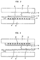
- FIGS 3, 4 and 5 depict alternative embodiments of implementations of the inventive actuation mechanism in a MEMS micro-relay.
- the MEMS micro-relay structure is formed by a mobile mechanical cantilever 12 having a thickness ranging from about 0.05 to 100 microns, lengths ranging from about 1 to 10000 microns, widths ranging from 0.1 to 10000 microns, and a mobile metallic electrode 20 carried at the free end and having a size ranging from about 0.1 to 5000 microns on a side. Actuation of the mechanical cantilever 12 causes the same to move up and down as desired.
- the mobile metallic electrode 20 makes electrical contact with one or more fixed metallic contacts 18 having a size ranging from about 0.1 to 5000 microns generally conforming to that of the mobile electrode 20, to thereby establish an electrical connection therebetween.
- the electrical connection is broken when the mechanical cantilever 12 is displaced or moves down to create a size gap or spacing ranging from about 0.05 to 200 microns between the metallic electrodes 18 and 20.
- the contact geometry may be rearranged to suit the particular application so that, for example, the mobile metallic electrode 20 lies on the lower side of cantilever 12, and the fixed metallic electrode 18 lies on substrate 26 beneath cantilever 12 ( Figure 5).
- cantilever 12 must when actuated be displaced downward to establish the connection, and upward to break it; in either case, the actuation mechanism should enable the mechanical cantilever 12 to move both up and down.
- the current carrying conductors 10 are fabricated for location beneath mechanical cantilever 12, and may be disposed or carried directly on substrate 26.
- the latchable magnetic material 14 is carried atop cantilever 12 together with a mobile electrode or contact 20.
- the second magnetic material 16 of a high coercive field is placed above the latchable magnetic material 14 and is adhered to another substrate 28 or other stationary surface using, for example, flip-chip bonding.
- the gap G between the two magnetic materials 14, 16 can range from about 0.05 to 500 microns.
- cantilever 12 As the magnetization direction of the soft magnetic material 14 atop cantilever 12 is switched by changing the flow direction of current I in the underlying conductors 10, the two magnetic materials exert either mutually attractive or repulsive forces, resulting in the respective upward or downward displacement and motion of mechanical cantilever 12.
- the upward motion of cantilever 12 causes mobile electrode 20 to contact fixed electrode 18 and thereby actuate a switched state of the MEMS device.
- Corresponding downward motion of cantilever 12 effects disconnection electrodes 20 and 18 from each other.
- Figure 4 depicts an alternative embodiment of the invention in which the current carrying conductors 10 and the soft magnetic thin-film material 24 are placed on the same substrate as the fixed electrode 18, and the second magnetic material 22 with a high coercive field is located on the mechanical cantilever 12.
- the actuation mechanism is nevertheless identical to that of the embodiment shown in Figure 3, despite the different relative locations of the two magnetic materials 22 and 24.
- Figure 5 depicts another alternative implementation of the actuating mechanism of the invention in which the flip-chip bonded substrate is eliminated by rearranging the electrodes and magnetic films.
- the mobile electrode 20 is placed on the lower surface of the mechanical cantilever 12 and the soft-latchable magnetic material 34 is arranged on an upper surface of cantilever 12.
- the fixed electrode 18, second magnetic material 32 and conductors 10 are all carried on the surface of substrate 26 beneath mechanical cantilever 12.
- the actuation mechanism is in any event the same as that described in the embodiment of Figure 3, except that it is the downward displacement or motion of cantilever 12 that brings electrodes 18 and 20 into physical and electrical contact.
Landscapes
- Physics & Mathematics (AREA)
- Electromagnetism (AREA)
- Engineering & Computer Science (AREA)
- Power Engineering (AREA)
- Micromachines (AREA)
- Electromagnets (AREA)
Abstract
Description
Claims (14)
- An actuation apparatus for a device including a mobile electrode having a first electrical contact and a stationary electrode having a second electrical contact, said actuation device comprising:a latchable magnetic material disposed on one of the mobile and stationary electrodes and having a magnetization direction that is changeable in response to exposure to an external magnetic field;at least one electrical conductor disposed in predeterminately spaced relation to said latchable magnetic material such that an external magnetic field created by passing electrical current through said at least one conductor exposes the latchable magnetic material to the created magnetic field to cause a change in the magnetization direction of said latchable magnetic material, said changed magnetization direction being maintained in the latchable magnetic material after the exposure to the created external magnetic field is discontinued; anda second magnetic material disposed on the other of the mobile and stationary electrodes and in predeterminately spaced relation to said latchable magnetic material so that said second magnetic material is one of attracted to and repelled from said latchable magnetic material in response to and as a function of the magnetization direction of said latchable magnetic material;
wherein the first and second electrical contacts may be selectively connected and disconnected by displacing the mobile electrode relative to the stationary electrode by selectively applying electrical current to said at least one conductor so as to create the external magnetic field to which the latchable magnetic material is exposed and thereby change the magnetization direction of said latchable magnetic material using the external magnetic field of the at least one conductor. - The apparatus in accordance with claim 1, wherein said second magnetic material is disposed on a plane on which said second electrical contact is disposed.
- The apparatus in accordance with claim 1, wherein the actuation apparatus comprises a mechanical relay.
- The apparatus in accordance with claim 1, wherein the actuation apparatus comprises a micro electro-mechanical system (MEMS) micro relay.
- The apparatus in accordance with claim 1, wherein passage of the electrical current passed through said at least one conductor in a first direction creates a first external magnetic field that results in attractive forces between the latchable magnetic material and the second magnetic material, and wherein passage of the electrical current through said at least one conductor in a second direction opposite said first direction creates a second external magnetic field opposite in direction to the first magnetic field that results in repulsive forces between the latchable magnetic material and the second magnetic material.
- The apparatus in accordance with claim 5, wherein the attractive forces cause relative movement of the mobile and stationary electrodes so that the first and second electrical contacts are relatively moved into contact with each other.
- The apparatus in accordance with claim 6, wherein the repulsive forces causes relative movement of the mobile and stationary electrodes so that the first and second electrical contacts are relatively moved out of contact with each other.
- The apparatus in accordance with claim 5, wherein the repulsive forces causes relative movement of the mobile and stationary electrodes so that the first and second electrical contacts are relatively moved into contact with each other.
- The apparatus in accordance with claim 8, wherein the attractive forces causes relative movement of the mobile and stationary electrodes so that the first and second electrical contacts are relatively moved out of contact with each other.
- The apparatus in accordance with claim 4, wherein said at least one conductor comprises a parallel conductor assembly in the MEMS micro-relay, wherein the magnetic field created by each of said at least one parallel conductor is one of locally combined and cancelled out so as to produce an in-plane magnetic field suitable for actuation of the latchable magnetic material.
- The apparatus in accordance with claim 1, wherein the magnetic field created by said at least one conductor comprises a coercive force in a range of 2-2000 Oersteds.
- The apparatus in accordance with claim 1, wherein the latchable magnetic material comprises a magnetic saturation in a range of 1000 - 24000 gauss.
- The apparatus in accordance with claim 1, wherein said latchable magnetic material comprises one selected from a group consisting of Ta-N, Fe-Cr-Ta-N, Fe-Zr-N, Co-Fe, Ni-Fe, Fe-Cr-Co, Fe based ferromagnetic films, Co based ferromagnetic films and Ni based ferromagnetic films.
- The apparatus in accordance with claim 1, wherein said second magnetic material comprises at least one permanent thin film material selected from a group consisting of Sm-Co, Nd-Fe-B, Fe-Al-Ni-Co, Fe-Cr-Co, Co-Fe-V and Cu-Ni-Fe.
Applications Claiming Priority (2)
| Application Number | Priority Date | Filing Date | Title |
|---|---|---|---|
| US418874 | 1999-10-15 | ||
| US09/418,874 US6124650A (en) | 1999-10-15 | 1999-10-15 | Non-volatile MEMS micro-relays using magnetic actuators |
Publications (3)
| Publication Number | Publication Date |
|---|---|
| EP1093141A2 true EP1093141A2 (en) | 2001-04-18 |
| EP1093141A3 EP1093141A3 (en) | 2003-04-09 |
| EP1093141B1 EP1093141B1 (en) | 2004-12-15 |
Family
ID=23659903
Family Applications (1)
| Application Number | Title | Priority Date | Filing Date |
|---|---|---|---|
| EP00308867A Expired - Lifetime EP1093141B1 (en) | 1999-10-15 | 2000-10-09 | Non-volatile mems micro-relays using magnetic actuators |
Country Status (5)
| Country | Link |
|---|---|
| US (1) | US6124650A (en) |
| EP (1) | EP1093141B1 (en) |
| JP (1) | JP4459419B2 (en) |
| CA (1) | CA2323025C (en) |
| DE (1) | DE60016692T2 (en) |
Cited By (1)
| Publication number | Priority date | Publication date | Assignee | Title |
|---|---|---|---|---|
| EP1254473B1 (en) * | 2000-02-02 | 2005-09-07 | Arizona State University | Electronically switching latching micro-magnetic relay and method of operating same |
Families Citing this family (77)
| Publication number | Priority date | Publication date | Assignee | Title |
|---|---|---|---|---|
| US6496612B1 (en) * | 1999-09-23 | 2002-12-17 | Arizona State University | Electronically latching micro-magnetic switches and method of operating same |
| US7027682B2 (en) | 1999-09-23 | 2006-04-11 | Arizona State University | Optical MEMS switching array with embedded beam-confining channels and method of operating same |
| US6853067B1 (en) | 1999-10-12 | 2005-02-08 | Microassembly Technologies, Inc. | Microelectromechanical systems using thermocompression bonding |
| US7057246B2 (en) * | 2000-08-23 | 2006-06-06 | Reflectivity, Inc | Transition metal dielectric alloy materials for MEMS |
| US20020096421A1 (en) * | 2000-11-29 | 2002-07-25 | Cohn Michael B. | MEMS device with integral packaging |
| US6785038B2 (en) | 2001-01-17 | 2004-08-31 | Optical Coating Laboratory, Inc. | Optical cross-connect with magnetic micro-electro-mechanical actuator cells |
| US6801681B2 (en) | 2001-01-17 | 2004-10-05 | Optical Coating Laboratory, Inc. | Optical switch with low-inertia micromirror |
| ES2282391T3 (en) * | 2001-01-18 | 2007-10-16 | Arizona State University | MICROMAGNETIC LOCK COMPUTER WITH REDUCED REQUIREMENTS FOR ALIGNMENT OF PERMANENT MAGNETS. |
| US6970616B2 (en) * | 2001-03-18 | 2005-11-29 | Touchdown Technologies, Inc. | Optical cross-connect assembly |
| US20020183011A1 (en) * | 2001-03-19 | 2002-12-05 | Superconductor Technologies, Inc. | Method and apparatus for combined receive and transmit subsystems in cellular communication systems |
| WO2002080207A1 (en) * | 2001-03-30 | 2002-10-10 | Arizona State University | Micro-machined radio frequency switches and method of operating the same |
| EP1383708A1 (en) * | 2001-04-17 | 2004-01-28 | Telefonaktiebolaget LM Ericsson (publ) | Printed circuit board integrated switch |
| EP1399939A4 (en) * | 2001-05-18 | 2006-11-15 | Microlab Inc | Micromagnetic latching switch packaging |
| CA2445464C (en) * | 2001-05-23 | 2008-08-05 | The Board Of Trustees Of The University Of Illinois | Raised on-chip inductor and method of manufacturing same |
| US20020196110A1 (en) * | 2001-05-29 | 2002-12-26 | Microlab, Inc. | Reconfigurable power transistor using latching micromagnetic switches |
| US6607305B2 (en) | 2001-06-04 | 2003-08-19 | Wisconsin Alumni Research Foundation | Bi-directional micromechanical latching linear actuator |
| FR2826504B1 (en) * | 2001-06-25 | 2003-09-12 | Commissariat Energie Atomique | MAGNETIC ACTUATOR WITH REDUCED RESPONSE TIME |
| US7057251B2 (en) * | 2001-07-20 | 2006-06-06 | Reflectivity, Inc | MEMS device made of transition metal-dielectric oxide materials |
| JP3750574B2 (en) * | 2001-08-16 | 2006-03-01 | 株式会社デンソー | Thin film electromagnet and switching element using the same |
| US6750745B1 (en) * | 2001-08-29 | 2004-06-15 | Magfusion Inc. | Micro magnetic switching apparatus and method |
| US20030173957A1 (en) * | 2001-08-29 | 2003-09-18 | Microlab, Inc. | Micro magnetic proximity sensor |
| US6778046B2 (en) | 2001-09-17 | 2004-08-17 | Magfusion Inc. | Latching micro magnetic relay packages and methods of packaging |
| US7301334B2 (en) * | 2001-09-17 | 2007-11-27 | Schneider Electric Industries Sas | Micro magnetic proximity sensor system |
| GB0123521D0 (en) * | 2001-10-01 | 2001-11-21 | Gill Michael J | Electrical apparatus |
| US6919784B2 (en) * | 2001-10-18 | 2005-07-19 | The Board Of Trustees Of The University Of Illinois | High cycle MEMS device |
| US20030107460A1 (en) * | 2001-12-10 | 2003-06-12 | Guanghua Huang | Low voltage MEM switch |
| US6754510B2 (en) * | 2001-12-13 | 2004-06-22 | Superconductor Technologies, Inc. | MEMS-based bypass system for use with a HTS RF receiver |
| US20030169135A1 (en) * | 2001-12-21 | 2003-09-11 | Jun Shen | Latching micro-magnetic switch array |
| US6836194B2 (en) * | 2001-12-21 | 2004-12-28 | Magfusion, Inc. | Components implemented using latching micro-magnetic switches |
| US20030179057A1 (en) * | 2002-01-08 | 2003-09-25 | Jun Shen | Packaging of a micro-magnetic switch with a patterned permanent magnet |
| KR100439423B1 (en) | 2002-01-16 | 2004-07-09 | 한국전자통신연구원 | Microelectromechanical actuators |
| US20030179058A1 (en) * | 2002-01-18 | 2003-09-25 | Microlab, Inc. | System and method for routing input signals using single pole single throw and single pole double throw latching micro-magnetic switches |
| US20030137374A1 (en) * | 2002-01-18 | 2003-07-24 | Meichun Ruan | Micro-Magnetic Latching switches with a three-dimensional solenoid coil |
| US20030222740A1 (en) * | 2002-03-18 | 2003-12-04 | Microlab, Inc. | Latching micro-magnetic switch with improved thermal reliability |
| US6753747B2 (en) * | 2002-04-01 | 2004-06-22 | Intel Corporation | Integrated microsprings for high speed switches |
| DE10214523B4 (en) * | 2002-04-02 | 2007-10-11 | Infineon Technologies Ag | Micromechanical device with magnetic actuator |
| US6924966B2 (en) * | 2002-05-29 | 2005-08-02 | Superconductor Technologies, Inc. | Spring loaded bi-stable MEMS switch |
| US6795697B2 (en) | 2002-07-05 | 2004-09-21 | Superconductor Technologies, Inc. | RF receiver switches |
| AU2003302019A1 (en) * | 2002-08-23 | 2004-06-15 | The Regents Of The University Of California | Improved microscale vacuum tube device and method for making same |
| AU2003304297A1 (en) * | 2002-08-23 | 2005-01-21 | Sungho Jin | Article comprising gated field emission structures with centralized nanowires and method for making the same |
| US7012266B2 (en) | 2002-08-23 | 2006-03-14 | Samsung Electronics Co., Ltd. | MEMS-based two-dimensional e-beam nano lithography device and method for making the same |
| US6998946B2 (en) * | 2002-09-17 | 2006-02-14 | The Board Of Trustees Of The University Of Illinois | High cycle deflection beam MEMS devices |
| AU2003272500A1 (en) * | 2002-09-18 | 2004-04-08 | Mark Goranson | Method of assembling a laminated electro-mechanical structure |
| US7202763B2 (en) * | 2002-09-25 | 2007-04-10 | Nxp B.V. | Micro-electromechanical switching device |
| US20040121505A1 (en) | 2002-09-30 | 2004-06-24 | Magfusion, Inc. | Method for fabricating a gold contact on a microswitch |
| US7202765B2 (en) | 2003-05-14 | 2007-04-10 | Schneider Electric Industries Sas | Latchable, magnetically actuated, ground plane-isolated radio frequency microswitch |
| US7202764B2 (en) * | 2003-07-08 | 2007-04-10 | International Business Machines Corporation | Noble metal contacts for micro-electromechanical switches |
| US7215229B2 (en) * | 2003-09-17 | 2007-05-08 | Schneider Electric Industries Sas | Laminated relays with multiple flexible contacts |
| JP4561072B2 (en) | 2003-09-30 | 2010-10-13 | 株式会社日立製作所 | Semiconductor device having MEMS switch |
| US7183884B2 (en) * | 2003-10-15 | 2007-02-27 | Schneider Electric Industries Sas | Micro magnetic non-latching switches and methods of making same |
| US20050083157A1 (en) * | 2003-10-15 | 2005-04-21 | Magfusion, Inc. | Micro magnetic latching switches and methods of making same |
| US7342473B2 (en) * | 2004-04-07 | 2008-03-11 | Schneider Electric Industries Sas | Method and apparatus for reducing cantilever stress in magnetically actuated relays |
| KR100574510B1 (en) * | 2004-05-11 | 2006-04-27 | 삼성전자주식회사 | Magnetic levitation structure using MEMS process and its manufacturing method |
| JP2006179252A (en) * | 2004-12-21 | 2006-07-06 | Fujitsu Component Ltd | Switch device |
| WO2007007206A2 (en) * | 2005-03-18 | 2007-01-18 | Simpler Networks, Inc. | Mems actuators and switches |
| US20060222871A1 (en) * | 2005-03-31 | 2006-10-05 | Bonhote Christian R | Method for lowering deposition stress, improving ductility, and enhancing lateral growth in electrodeposited iron-containing alloys |
| US7692521B1 (en) * | 2005-05-12 | 2010-04-06 | Microassembly Technologies, Inc. | High force MEMS device |
| US7528691B2 (en) * | 2005-08-26 | 2009-05-05 | Innovative Micro Technology | Dual substrate electrostatic MEMS switch with hermetic seal and method of manufacture |
| US7482899B2 (en) * | 2005-10-02 | 2009-01-27 | Jun Shen | Electromechanical latching relay and method of operating same |
| US20070171205A1 (en) * | 2006-01-24 | 2007-07-26 | Steinberg Dan A | Keyboard having magnet-actuted switches |
| US8174343B2 (en) * | 2006-09-24 | 2012-05-08 | Magvention (Suzhou) Ltd. | Electromechanical relay and method of making same |
| US20080197964A1 (en) * | 2007-02-21 | 2008-08-21 | Simpler Networks Inc. | Mems actuators and switches |
| US7893798B2 (en) * | 2007-05-09 | 2011-02-22 | Innovative Micro Technology | Dual substrate MEMS plate switch and method of manufacture |
| US8068002B2 (en) * | 2008-04-22 | 2011-11-29 | Magvention (Suzhou), Ltd. | Coupled electromechanical relay and method of operating same |
| US8445306B2 (en) * | 2008-12-24 | 2013-05-21 | International Business Machines Corporation | Hybrid MEMS RF switch and method of fabricating same |
| US8143978B2 (en) * | 2009-02-23 | 2012-03-27 | Magvention (Suzhou), Ltd. | Electromechanical relay and method of operating same |
| US8159320B2 (en) * | 2009-09-14 | 2012-04-17 | Meichun Ruan | Latching micro-magnetic relay and method of operating same |
| DE102010002818B4 (en) * | 2010-03-12 | 2017-08-31 | Robert Bosch Gmbh | Method for producing a micromechanical component |
| US8635765B2 (en) | 2011-06-15 | 2014-01-28 | International Business Machines Corporation | Method of forming micro-electrical-mechanical structure (MEMS) |
| US20130207754A1 (en) * | 2012-02-14 | 2013-08-15 | U.S. Government As Represented By The Secretary Of The Army | Magnetic flux switch |
| DE102012216997A1 (en) * | 2012-09-21 | 2014-03-27 | M-Invest GmbH | Electrical switching element i.e. reed contact, for e.g. contactless switch used in pacemaker, has contact pad contacted by deflection region of extension during deflecting deflection region in direction by external magnetic field |
| KR101444552B1 (en) * | 2012-12-21 | 2014-10-30 | 삼성전기주식회사 | Magnetic sheet, method for manufacturing the same, and contactless power transmission device including the same |
| US9105841B2 (en) * | 2013-03-12 | 2015-08-11 | International Business Machines Corporation | Forming magnetic microelectromechanical inductive components |
| US9926193B2 (en) | 2014-06-27 | 2018-03-27 | Intel Corporation | Magnetic nanomechanical devices for stiction compensation |
| US10132699B1 (en) * | 2014-10-06 | 2018-11-20 | National Technology & Engineering Solutions Of Sandia, Llc | Electrodeposition processes for magnetostrictive resonators |
| US10825628B2 (en) * | 2017-07-17 | 2020-11-03 | Analog Devices Global Unlimited Company | Electromagnetically actuated microelectromechanical switch |
| JP6950613B2 (en) * | 2018-04-11 | 2021-10-13 | Tdk株式会社 | Magnetically actuated MEMS switch |
Family Cites Families (8)
| Publication number | Priority date | Publication date | Assignee | Title |
|---|---|---|---|---|
| US5206983A (en) * | 1991-06-24 | 1993-05-04 | Wisconsin Alumni Research Foundation | Method of manufacturing micromechanical devices |
| US5629918A (en) * | 1995-01-20 | 1997-05-13 | The Regents Of The University Of California | Electromagnetically actuated micromachined flap |
| US5644177A (en) * | 1995-02-23 | 1997-07-01 | Wisconsin Alumni Research Foundation | Micromechanical magnetically actuated devices |
| FR2742917B1 (en) * | 1995-12-22 | 1998-02-13 | Suisse Electronique Microtech | MINIATURE DEVICE FOR EXECUTING A PREDETERMINED FUNCTION, ESPECIALLY MICRORELAIS |
| US5945898A (en) * | 1996-05-31 | 1999-08-31 | The Regents Of The University Of California | Magnetic microactuator |
| JP2998680B2 (en) * | 1997-02-27 | 2000-01-11 | 日本電気株式会社 | High frequency relay |
| CH691559A5 (en) * | 1997-04-21 | 2001-08-15 | Asulab Sa | magnetic micro-switch and its production process. |
| DE19813128A1 (en) * | 1998-03-25 | 1999-09-30 | Kuhnke Gmbh Kg H | Electromagnetic relay for controlling electrical currents and voltages can switch high levels of electrical power with adequate contact separation and minimal control power and internal heat generation |
-
1999
- 1999-10-15 US US09/418,874 patent/US6124650A/en not_active Expired - Lifetime
-
2000
- 2000-10-06 CA CA002323025A patent/CA2323025C/en not_active Expired - Fee Related
- 2000-10-09 EP EP00308867A patent/EP1093141B1/en not_active Expired - Lifetime
- 2000-10-09 DE DE60016692T patent/DE60016692T2/en not_active Expired - Lifetime
- 2000-10-16 JP JP2000314633A patent/JP4459419B2/en not_active Expired - Fee Related
Cited By (1)
| Publication number | Priority date | Publication date | Assignee | Title |
|---|---|---|---|---|
| EP1254473B1 (en) * | 2000-02-02 | 2005-09-07 | Arizona State University | Electronically switching latching micro-magnetic relay and method of operating same |
Also Published As
| Publication number | Publication date |
|---|---|
| JP4459419B2 (en) | 2010-04-28 |
| CA2323025C (en) | 2003-07-29 |
| EP1093141B1 (en) | 2004-12-15 |
| DE60016692T2 (en) | 2005-12-15 |
| EP1093141A3 (en) | 2003-04-09 |
| JP2001176369A (en) | 2001-06-29 |
| CA2323025A1 (en) | 2001-04-15 |
| US6124650A (en) | 2000-09-26 |
| DE60016692D1 (en) | 2005-01-20 |
Similar Documents
| Publication | Publication Date | Title |
|---|---|---|
| CA2323025C (en) | Non-volatile mems micro-relays using magnetic actuators | |
| KR100474536B1 (en) | Electronically switching latching micro-magnetic relay and method of operating same | |
| US6366186B1 (en) | Mems magnetically actuated switches and associated switching arrays | |
| KR100298254B1 (en) | Magnetic relay system and method for microfabrication manufacturing B | |
| Cugat et al. | Magnetic micro-actuators and systems (MAGMAS) | |
| US5889452A (en) | Miniature device for executing a predetermined function, in particular microrelay | |
| Niarchos | Magnetic MEMS: key issues and some applications | |
| Chin | Permanent magnet films for applications in microelectromechanical systems | |
| TW500929B (en) | Electronically latching micro-magnetic switches, network thereof and method of operating same | |
| Fullin et al. | A new basic technology for magnetic micro-actuators | |
| US7106159B2 (en) | Mobile magnet actuator | |
| CN101253593B (en) | Electromechanical latching relay and method of operating same | |
| US7142078B2 (en) | Magnetic levitation actuator | |
| US8581678B2 (en) | Method and apparatus for electromagnetic actuation | |
| US20060082427A1 (en) | Method and apparatus for reducing cantilever stress in magnetically actuated relays | |
| EP1667187B1 (en) | Passive magnetic latch | |
| US20080135956A1 (en) | Articles and assembly for magnetically directed self assembly and methods of manufacture | |
| US20040113732A1 (en) | Bistable magnetic actuator | |
| KR101023581B1 (en) | Micro system with electromagnet control | |
| Dempsey | Hard magnetic materials for MEMS applications | |
| US5742012A (en) | Switching field | |
| US20140077906A1 (en) | Microswitch having an integrated electromagnetic coil | |
| US20020196112A1 (en) | Electronically switching latching micro-magnetic relay and method of operating same | |
| US3919676A (en) | Permanent-magnet type relay | |
| CN1694190A (en) | Integrated permanent magnet bistable micro-electromagnetic driver |
Legal Events
| Date | Code | Title | Description |
|---|---|---|---|
| PUAI | Public reference made under article 153(3) epc to a published international application that has entered the european phase |
Free format text: ORIGINAL CODE: 0009012 |
|
| AK | Designated contracting states |
Kind code of ref document: A2 Designated state(s): AT BE CH CY DE DK ES FI FR GB GR IE IT LI LU MC NL PT SE |
|
| AX | Request for extension of the european patent |
Free format text: AL;LT;LV;MK;RO;SI |
|
| PUAL | Search report despatched |
Free format text: ORIGINAL CODE: 0009013 |
|
| AK | Designated contracting states |
Designated state(s): AT BE CH CY DE DK ES FI FR GB GR IE IT LI LU MC NL PT SE Kind code of ref document: A3 Designated state(s): AT BE CH CY DE DK ES FI FR GB GR IE IT LI LU MC NL PT SE |
|
| AX | Request for extension of the european patent |
Extension state: AL LT LV MK RO SI |
|
| 17P | Request for examination filed |
Effective date: 20030929 |
|
| 17Q | First examination report despatched |
Effective date: 20031023 |
|
| AKX | Designation fees paid |
Designated state(s): DE FR GB |
|
| GRAP | Despatch of communication of intention to grant a patent |
Free format text: ORIGINAL CODE: EPIDOSNIGR1 |
|
| GRAS | Grant fee paid |
Free format text: ORIGINAL CODE: EPIDOSNIGR3 |
|
| GRAA | (expected) grant |
Free format text: ORIGINAL CODE: 0009210 |
|
| AK | Designated contracting states |
Kind code of ref document: B1 Designated state(s): DE FR GB |
|
| REG | Reference to a national code |
Ref country code: GB Ref legal event code: FG4D |
|
| REG | Reference to a national code |
Ref country code: IE Ref legal event code: FG4D |
|
| REF | Corresponds to: |
Ref document number: 60016692 Country of ref document: DE Date of ref document: 20050120 Kind code of ref document: P |
|
| PLBE | No opposition filed within time limit |
Free format text: ORIGINAL CODE: 0009261 |
|
| STAA | Information on the status of an ep patent application or granted ep patent |
Free format text: STATUS: NO OPPOSITION FILED WITHIN TIME LIMIT |
|
| ET | Fr: translation filed | ||
| 26N | No opposition filed |
Effective date: 20050916 |
|
| REG | Reference to a national code |
Ref country code: GB Ref legal event code: 732E Free format text: REGISTERED BETWEEN 20131107 AND 20131113 |
|
| REG | Reference to a national code |
Ref country code: FR Ref legal event code: CD Owner name: ALCATEL-LUCENT USA INC. Effective date: 20131122 |
|
| REG | Reference to a national code |
Ref country code: FR Ref legal event code: GC Effective date: 20140410 |
|
| REG | Reference to a national code |
Ref country code: FR Ref legal event code: RG Effective date: 20141015 |
|
| REG | Reference to a national code |
Ref country code: FR Ref legal event code: PLFP Year of fee payment: 16 |
|
| REG | Reference to a national code |
Ref country code: FR Ref legal event code: PLFP Year of fee payment: 17 |
|
| PGFP | Annual fee paid to national office [announced via postgrant information from national office to epo] |
Ref country code: FR Payment date: 20161020 Year of fee payment: 17 Ref country code: DE Payment date: 20161020 Year of fee payment: 17 Ref country code: GB Payment date: 20161020 Year of fee payment: 17 |
|
| REG | Reference to a national code |
Ref country code: DE Ref legal event code: R119 Ref document number: 60016692 Country of ref document: DE |
|
| GBPC | Gb: european patent ceased through non-payment of renewal fee |
Effective date: 20171009 |
|
| REG | Reference to a national code |
Ref country code: FR Ref legal event code: ST Effective date: 20180629 |
|
| PG25 | Lapsed in a contracting state [announced via postgrant information from national office to epo] |
Ref country code: GB Free format text: LAPSE BECAUSE OF NON-PAYMENT OF DUE FEES Effective date: 20171009 Ref country code: DE Free format text: LAPSE BECAUSE OF NON-PAYMENT OF DUE FEES Effective date: 20180501 |
|
| PG25 | Lapsed in a contracting state [announced via postgrant information from national office to epo] |
Ref country code: FR Free format text: LAPSE BECAUSE OF NON-PAYMENT OF DUE FEES Effective date: 20171031 |
|
| REG | Reference to a national code |
Ref country code: DE Ref legal event code: R081 Ref document number: 60016692 Country of ref document: DE Owner name: WSOU INVESTMENTS, LLC, LOS ANGELES, US Free format text: FORMER OWNER: LUCENT TECHNOLOGIES INC., MURRAY HILL, N.J., US |