EP1091567A2 - Charge transfer device, solid state image pickup device using the same, and control method - Google Patents
Charge transfer device, solid state image pickup device using the same, and control method Download PDFInfo
- Publication number
- EP1091567A2 EP1091567A2 EP00121321A EP00121321A EP1091567A2 EP 1091567 A2 EP1091567 A2 EP 1091567A2 EP 00121321 A EP00121321 A EP 00121321A EP 00121321 A EP00121321 A EP 00121321A EP 1091567 A2 EP1091567 A2 EP 1091567A2
- Authority
- EP
- European Patent Office
- Prior art keywords
- charge transfer
- charges
- transfer path
- horizontal
- charge
- Prior art date
- Legal status (The legal status is an assumption and is not a legal conclusion. Google has not performed a legal analysis and makes no representation as to the accuracy of the status listed.)
- Ceased
Links
- 238000000034 method Methods 0.000 title claims description 58
- 239000007787 solid Substances 0.000 title claims description 34
- 239000004065 semiconductor Substances 0.000 claims abstract description 59
- 239000000758 substrate Substances 0.000 claims abstract description 21
- 238000006243 chemical reaction Methods 0.000 claims description 47
- 238000009792 diffusion process Methods 0.000 claims description 9
- 230000004888 barrier function Effects 0.000 claims description 7
- 230000001419 dependent effect Effects 0.000 claims 1
- 239000010410 layer Substances 0.000 description 39
- 229910021420 polycrystalline silicon Inorganic materials 0.000 description 15
- 229920005591 polysilicon Polymers 0.000 description 15
- 239000012535 impurity Substances 0.000 description 5
- 230000004048 modification Effects 0.000 description 4
- 238000012986 modification Methods 0.000 description 4
- 238000005036 potential barrier Methods 0.000 description 4
- CNQCVBJFEGMYDW-UHFFFAOYSA-N lawrencium atom Chemical compound [Lr] CNQCVBJFEGMYDW-UHFFFAOYSA-N 0.000 description 2
- 238000001514 detection method Methods 0.000 description 1
- 238000010586 diagram Methods 0.000 description 1
- 239000011229 interlayer Substances 0.000 description 1
- 230000002035 prolonged effect Effects 0.000 description 1
- 238000011946 reduction process Methods 0.000 description 1
- 238000005070 sampling Methods 0.000 description 1
- 238000000638 solvent extraction Methods 0.000 description 1
- 239000002344 surface layer Substances 0.000 description 1
Images







Classifications
-
- H—ELECTRICITY
- H10—SEMICONDUCTOR DEVICES; ELECTRIC SOLID-STATE DEVICES NOT OTHERWISE PROVIDED FOR
- H10D—INORGANIC ELECTRIC SEMICONDUCTOR DEVICES
- H10D44/00—Charge transfer devices
- H10D44/40—Charge-coupled devices [CCD]
- H10D44/45—Charge-coupled devices [CCD] having field effect produced by insulated gate electrodes
- H10D44/454—Output structures
-
- H—ELECTRICITY
- H04—ELECTRIC COMMUNICATION TECHNIQUE
- H04N—PICTORIAL COMMUNICATION, e.g. TELEVISION
- H04N25/00—Circuitry of solid-state image sensors [SSIS]; Control thereof
- H04N25/40—Extracting pixel data from image sensors by controlling scanning circuits, e.g. by modifying the number of pixels sampled or to be sampled
- H04N25/46—Extracting pixel data from image sensors by controlling scanning circuits, e.g. by modifying the number of pixels sampled or to be sampled by combining or binning pixels
-
- H—ELECTRICITY
- H04—ELECTRIC COMMUNICATION TECHNIQUE
- H04N—PICTORIAL COMMUNICATION, e.g. TELEVISION
- H04N25/00—Circuitry of solid-state image sensors [SSIS]; Control thereof
- H04N25/70—SSIS architectures; Circuits associated therewith
-
- H—ELECTRICITY
- H04—ELECTRIC COMMUNICATION TECHNIQUE
- H04N—PICTORIAL COMMUNICATION, e.g. TELEVISION
- H04N25/00—Circuitry of solid-state image sensors [SSIS]; Control thereof
- H04N25/70—SSIS architectures; Circuits associated therewith
- H04N25/71—Charge-coupled device [CCD] sensors; Charge-transfer registers specially adapted for CCD sensors
- H04N25/73—Charge-coupled device [CCD] sensors; Charge-transfer registers specially adapted for CCD sensors using interline transfer [IT]
-
- H—ELECTRICITY
- H04—ELECTRIC COMMUNICATION TECHNIQUE
- H04N—PICTORIAL COMMUNICATION, e.g. TELEVISION
- H04N25/00—Circuitry of solid-state image sensors [SSIS]; Control thereof
- H04N25/70—SSIS architectures; Circuits associated therewith
- H04N25/71—Charge-coupled device [CCD] sensors; Charge-transfer registers specially adapted for CCD sensors
- H04N25/745—Circuitry for generating timing or clock signals
-
- H—ELECTRICITY
- H10—SEMICONDUCTOR DEVICES; ELECTRIC SOLID-STATE DEVICES NOT OTHERWISE PROVIDED FOR
- H10F—INORGANIC SEMICONDUCTOR DEVICES SENSITIVE TO INFRARED RADIATION, LIGHT, ELECTROMAGNETIC RADIATION OF SHORTER WAVELENGTH OR CORPUSCULAR RADIATION
- H10F39/00—Integrated devices, or assemblies of multiple devices, comprising at least one element covered by group H10F30/00, e.g. radiation detectors comprising photodiode arrays
- H10F39/10—Integrated devices
- H10F39/12—Image sensors
- H10F39/15—Charge-coupled device [CCD] image sensors
- H10F39/153—Two-dimensional or three-dimensional array CCD image sensors
- H10F39/1534—Interline transfer
-
- H—ELECTRICITY
- H04—ELECTRIC COMMUNICATION TECHNIQUE
- H04N—PICTORIAL COMMUNICATION, e.g. TELEVISION
- H04N23/00—Cameras or camera modules comprising electronic image sensors; Control thereof
- H04N23/80—Camera processing pipelines; Components thereof
- H04N23/84—Camera processing pipelines; Components thereof for processing colour signals
-
- H—ELECTRICITY
- H04—ELECTRIC COMMUNICATION TECHNIQUE
- H04N—PICTORIAL COMMUNICATION, e.g. TELEVISION
- H04N25/00—Circuitry of solid-state image sensors [SSIS]; Control thereof
- H04N25/10—Circuitry of solid-state image sensors [SSIS]; Control thereof for transforming different wavelengths into image signals
- H04N25/11—Arrangement of colour filter arrays [CFA]; Filter mosaics
- H04N25/13—Arrangement of colour filter arrays [CFA]; Filter mosaics characterised by the spectral characteristics of the filter elements
- H04N25/134—Arrangement of colour filter arrays [CFA]; Filter mosaics characterised by the spectral characteristics of the filter elements based on three different wavelength filter elements
Definitions
- the present invention relates to a charge transfer device, a solid state image pickup device, and a control method for a solid state image pickup device.
- Figs. 15A and 15B show an example of a general charge transfer device.
- Fig. 15A is a plan view and
- Fig. 15B is a schematic cross sectional view.
- a charge transfer device X has: a semiconductor substrate 101 having a principal surface layer of a p-type or an i-type; an n-type semiconductor layer 105 formed on the surface of the semiconductor substrate 101; charge transfer electrodes 121 of polysilicon formed on an insulating film 115 on the n-type semiconductor layer 105; and a pulse signal generator 125 for applying pulse voltages to the charge transfer electrodes.
- the charge transfer electrodes 121 include first charge transfer electrodes 121-1, 121-3, 121-5,... made of a first layer of polysilicon and second charge transfer electrodes 121-2, 121-4, 121-6,... made of a second layer of polysilicon.
- the first and second charge transfer electrodes are disposed alternately in a horizontal direction.
- the regions of the n-type semiconductor layer 105 under the first charge transfer electrodes 121-1, 121-3, 121-5,... made of the first layer polysilicon have a low n-type impurity concentration, forming potential barriers (B).
- the regions of the n-type semiconductor layer 105 under the second charge transfer electrodes 121-2, 121-4, 121-6,... made of the second layer polysilicon have a high n-type impurity concentration, forming potential wells (W).
- First and second two charge transfer electrodes 121 adjacent to each other in the horizontal direction e.g., the first and second charge transfer electrodes 121-1 and 121-2, or 121-3 and 121-4, are connected in common.
- a pulse signal ⁇ 2 is applied from the pulse signal generator 125 to the commonly connected charge transfer electrodes 121-1 and 121-2.
- a pulse signal ⁇ 1 is applied from the pulse signal generator 125 to the commonly connected charge transfer electrodes 121-3 and 121-4.
- pairs of first and second two adjacent charge transfer electrodes disposed alternately in the horizontal direction are alternately applied with pulse signals ⁇ 2, ⁇ 1, ⁇ 2, ⁇ 1,... from the pulse signal generator 125.
- Fig. 16 shows the waveforms of pulse signals generated from the pulse signal generator 125 (Fig. 15B).
- the pulse signal ⁇ 1 has a waveform with a low level and a high level being set alternately.
- the pulse signal ⁇ 2 has a waveform opposite in phase to the pulse signal ⁇ 1.
- charges may be transferred by a three-phase drive method, a four-phase drive method or the like.
- a pair of first and second two charge transfer electrodes 121 constitutes one charge transfer stage.
- each charge transfer stage is fixed.
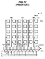
- Fig. 17 is a plan view showing a solid state image pickup device A using the charge transfer device X shown in Figs. 15A and 15B.
- the solid state image pickup device A shown in Fig. 17 has: a plurality of photoelectric conversion elements 103 disposed regularly on a two-dimensional plane of the surface of a semiconductor substrate 101; a plurality of vertical charge transfer paths 105 for reading signal charges accumulated in the photoelectric conversion elements 103 and sequentially transferring the read charges in a column direction; a horizontal charge transfer path 107 connected to one end of the vertical charge transfer paths 105 for transferring charges transferred from the vertical charge transfer paths 105 in the horizontal direction; and an output amplifier 111 for amplifying the charges transferred from the horizontal charge transfer path 107 and outputting the amplified charges.
- a read gate 103a is formed between the photoelectric conversion element 103 and vertical charge transfer path 105 to read charges accumulated in the photoelectric conversion element 103 to the vertical charge transfer path 105. Charges are transferred in the vertical charge transfer path 105 toward the horizontal charge transfer path 107.
- the charge transfer device X is used as the horizontal charge transfer path 107.
- One end of the vertical charge transfer path 105 is connected to the high concentration n-type semiconductor layer 105a forming a well layer in the horizontal charge transfer path 107.
- the two-phase drive type charge transfer device described above is driven by two-phase drive pulses.
- Conventional three-phase or four-phase drive type charge transfer devices not using barrier layers and well layers transfer charges by three-phase or four-phase drive pulses, and cannot transfer charges by different methods.
- two charge transfer electrodes constitute one charge transfer stage and a geometrical length of one charge transfer stage is fixed.
- Such constriction poses some problem when the charge transfer device is used as the horizontal charge transfer path of a solid state image pickup device.
- one charge transfer stage of the horizontal charge transfer path is provided for each vertical charge transfer path in order to transfer all image signals from the vertical charge transfer paths to the horizontal charge transfer path.
- a charge transfer device comprising: a semiconductor substrate; a charge transfer path formed in the semiconductor substrate and made of a first conductivity type semiconductor layer; a plurality of charge transfer electrodes formed near above the charge transfer path; and a first pulse signal generator circuit for applying either a first pulse signal train for n-phase (n being an integer larger than 1) driving of charges in the charge transfer path to the charge transfer electrodes or a second pulse signal train for (n + 1)-phase driving of charges in the charge transfer path to the charge transfer electrodes.
- a method of reading a solid state image pickup device including: a semiconductor substrate; a plurality of photoelectric conversion elements regularly disposed in row and column directions on the semiconductor substrate; a plurality of vertical charge transfer paths extending in a vertical direction and each disposed adjacent to each of a plurality of photoelectric conversion element columns regularly disposed in the column direction; a read gate formed between each photoelectric conversion element and a corresponding vertical charge transfer path for transferring charges accumulated in the photoelectric conversion element to the vertical charge transfer path; a horizontal charge transfer path formed at one ends of the plurality of vertical charge transfer paths for transferring charges in a horizontal direction; and an output amplifier for amplifying charges transferred by the horizontal charge transfer path and outputting the amplified charges, the horizontal charge transfer path including: a charge transfer path formed in the semiconductor substrate and made of a first conductivity type semiconductor layer, the charge transfer path having first barrier layers having a high potential and second well layers having a low potential, disposed alternately;
- a length of one charge transfer stage of a charge transfer device can be changed with the phase of drive pulses.
- a monitor image taking operation of an electronic still camera such as 1/2, 1/3 and 1/4 thinning operations, can be realized without empty charge transfer so that power consumption can be reduced.
- a capacity of signal transfer can be increased greatly by a multiple-phase drive method.
- a charge transfer device according to the first embodiment of the invention will be described with reference to Fig. 1, Figs. 2A and 2B and Fig. 3.
- Fig. 1 is a plan view of the charge transfer device of the first embodiment
- Fig. 2 shows a cross sectional structure of the charge transfer device, with illustrations how charges are transferred
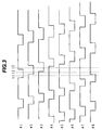
- Fig. 3 shows the waveforms of drive pulses.
- a charge transfer device A has: a semiconductor substrate 1; a first conductivity type (n-type) semiconductor layer 7 formed on the surface of the semiconductor substrate 1; charge transfer electrodes 21 of polysilicon formed on an insulating film 15 on the semiconductor layer 7; and pulse signal generators 25 (25a, 25b) for applying pulse voltages to the charge transfer electrodes.
- the charge transfer electrodes 21 include generally first charge transfer electrodes 21-1, 21-3, 21-5,... made of first layer polysilicon and second charge transfer electrodes 21-2, 21-4, 21-6,... made of second layer polysilicon.
- the first and second charge transfer electrodes are disposed alternately in a horizontal direction.
- the n-type semiconductor layer 7 has an approximately uniform thickness, forming impurity doped regions.
- a pulse signal ⁇ 1 is applied from the pulse signal generator 25 (25a) to the charge transfer electrode 21-1.
- a pulse signal ⁇ 2 is applied from the pulse signal generator 25 (25a) to the charge transfer electrode 21-2 adjacent to the charge transfer electrode 21-1.
- a pulse signal ⁇ 3 is applied from the pulse signal generator 25 (25a) to the charge transfer electrode 21-3 adjacent to the charge transfer electrode 21-2.
- a pulse signal ⁇ 4 is applied from the pulse signal generator 25 (25a) to the charge transfer electrode 21-4 adjacent to the charge transfer electrode 21-3.
- the pulse signals ⁇ 1 to ⁇ 4 are applied to the adjacent charge transfer electrodes 21-5 to 21-8.
- the pulse signals ⁇ 1 to ⁇ 4 are called a first pulse signal train.
- Different pulse signals ⁇ 1 to ⁇ 8 are applied from the pulse signal generator 25 (25b) to the same charge transfer electrodes 21 of the charge transfer electrode group G1.
- the pulse signals ⁇ 1 to ⁇ 8 are called a second pulse signal train.
- the first pulse signal train (four-phase drive pulses) is applied to the transfer electrodes 21 of the charge transfer device A, charges in the charge transfer device are transferred by a four-phase drive method.
- an n-phase (n is an integer larger than 2) drive method such as a two-phase or a three-phase drive method may be used.
- the length of a charge transfer stage for the eight-phase drive method by applying the second pulse signal train is two times that for the four-phase drive method by applying the first pulse signal train.
- the length of a charge transfer stage for an n-phase drive method (n is a positive integer) is n/4 times that for the four-phase drive method.
- an (n + 1)-phase or (n x m)-phase drive method may be used (m is an integer larger than 1).
- Fig. 3 shows the voltage waveforms of the second pulse signal train generated by the pulse signal generator 25.
- the drive pulses ⁇ 1 to ⁇ 8 rise from the low level to the high level and fall from the high level to the low level, in the sequential order of ⁇ 1 to ⁇ 8, as seen along the abscissa (time) in Fig. 3.
- Fig. 2 shows the charge distribution in the charge transfer device A at times t1, t2 and t3 shown in Fig. 3.
- Charge signals transferred from the vertical charge transfer paths are transferred in the horizontal direction sequentially from time t1 to time t3.
- a ratio of empty charge transfer stages to total stages is low. The charge transfer efficiency is therefore improved. Since eight charge transfer electrodes are driven during one period, a charge transfer is speeded up.
- the pulse signal generators for generating the first and second pulse signal trains may be formed in the same circuit or in separate circuits.
- the pulse signal generators may be formed in the same semiconductor substrate or in different substrates (chips).
- Figs. 4A and 4B and Fig. 5 show a charge transfer device according to the second embodiment of the invention.
- Fig. 4 shows the cross sectional structure of the charge transfer device, with an illustration how charges are transferred
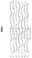
- Fig. 5 shows the waveforms of a pulse signal train applied to transfer electrodes.
- a final transfer electrode FE As shown in Fig. 4, formed on the final output side of a horizontal charge transfer path 37 are a final transfer electrode FE, an output gate OG, a floating diffusion FD region (charge detecting layer), a reset gate RS, and a reset drain RD.
- the reset gate RS is an electrode used when charges accumulated in the floating diffusion FD region are reset to an initial value. Reset charges are drained to the reset drain RD.
- the fundamental structure of the second embodiment is similar to that of the charge transfer device of the first embodiment.
- a difference in the charge transfer device of the second embodiment is that the final transfer electrode FE is formed adjacent to the final charge transfer stage of the horizontal charge transfer path.
- Charges in the horizontal charge transfer path 37 are transferred toward the floating diffusion FD region by a six-phase drive method.
- a signal ⁇ 1L is applied to the final transfer electrode FE.
- Charges are stored in a well region (n-type semiconductor layer) under the final transfer electrode FE.
- Fig. 5 shows the waveforms of pulse signals applied to charge transfer electrodes.
- the pulse signals ⁇ 1 to ⁇ 6 are applied to charge transfer electrodes to transfer signal charges in the horizontal charge transfer path by a six-phase drive method.
- the pulse signal ⁇ 1L takes a high level, charges are stored in a well of a semiconductor region (*n-type semiconductor layer) under the final transfer electrode FE, and as the pulse signal ⁇ 1L takes a low level, the stored charges are transferred to the floating diffusion FD region.
- Fig. 4 also illustrates how charges are transferred at times t1 to t7 shown in Fig. 5.
- the drive pulse ⁇ 1L takes a high level voltage.
- the potential of the semiconductor region (n-type semiconductor layer) under the final transfer electrode FE lowers to form a potential well.
- the signal ⁇ 1 takes the low level voltage
- the signals ⁇ 2 to ⁇ 5 takes a high level voltage
- the signal ⁇ 6 takes the low level voltage.
- Charges are stored in the semiconductor regions under the horizontal charge transfer electrodes applied with the high level voltage. Since the signal ⁇ 6 takes the low level, a potential barrier is formed in the semiconductor region of the final charge transfer stage of the horizontal charge transfer path. The stored charges are not transferred to the semiconductor region under the final transfer electrode FE.
- the signal ⁇ 2 takes the low level and the signal ⁇ 6 takes the high level.
- the potential barrier formed in the semiconductor region of the final charge transfer stage of the horizontal charge transfer path disappears.
- the charges stored in the final charge transfer stage of the horizontal charge transfer path are therefore transferred to the semiconductor region under the final transfer electrode FE.
- the transferred charges are stored in the well formed in the semiconductor region.
- the signal ⁇ 3 takes the low level. Charges in the horizontal charge transfer path are transferred to the semiconductor region under the final transfer electrode FE. The transferred charges are stored in the well formed in the semiconductor region.
- the signal ⁇ 4 takes the low level. Charges in the horizontal charge transfer path are transferred to the semiconductor region under the final transfer electrode FE. The transferred charges are stored in the well formed in the semiconductor region.
- the signal ⁇ 5 takes the low level. Similar to the above, charges in the horizontal charge transfer path are transferred to the semiconductor region under the final transfer electrode FE and stored in the well.
- the signal ⁇ 6 takes the low level. Similar to the above, charges in the horizontal charge transfer path are transferred to the semiconductor region under the final transfer electrode FE and stored in the well.
- a high level voltage is applied to the output gate OG, and the signal ⁇ 1L takes the low level.
- the charges stored in the semiconductor region under the final transfer gate FE are transferred to the floating diffusion FD region because of a raised potential in this semiconductor region.
- the horizontal charge transfer path 37 is driven by the six-phase drive method, charges are transferred to the charge detecting layer only when the sixth phase drive pulse is applied.
- the output signal waveform has a frequency different from that when charges in the horizontal charge transfer path 37 are transferred by the two-phase drive method, the data rate is equal.
- the charges temporarily stored in the semiconductor region under the final transfer electrode FE can be transferred to the floating diffusion FD region at the same time.
- Signal detection, output timings and an output period can be set almost arbitrarily, and an output suitable for signal processing can be obtained.
- a noise reduction process such as a CDS process (process by a correlation double sampling circuit) can be executed.
- Fig. 6 is a plan view of the charge transfer device
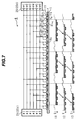
- Fig. 7 shows the cross sectional structure of the charge transfer device, with an illustration as to how charges are transferred
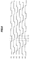
- Fig. 8 shows the waveforms of drive pulses.
- a charge transfer device B has: similar to the charge transfer device A described earlier, a semiconductor substrate 1; an n-type semiconductor layer 7 formed on the surface of the semiconductor substrate 1; charge transfer electrodes 21 of polysilicon formed on an interlayer insulating film 15 on the n-type semiconductor layer 7; and pulse signal generators 25 (25c, 25d) for applying pulse voltages to the charge transfer electrodes.
- the charge transfer electrodes 21 include first charge transfer electrodes 21-1, 21-3, 21-5,... made of first layer polysilicon and second charge transfer electrodes 21-2, 21-4, 21-6,... made of second layer polysilicon.
- the first and second charge transfer electrodes are disposed alternately in the horizontal direction.
- the regions of the n-type semiconductor layer 7 under the first charge transfer electrodes 21-1, 21-3, 21-5,... made of the first layer polysilicon have a low n-type impurity concentration, forming potential barriers (B).
- the regions of the n-type semiconductor layer 7 under the second charge transfer electrodes 21-2, 21-4, 21-6,... made of the second layer polysilicon have a high n-type impurity concentration, forming potential wells (W).
- First and second two charge transfer electrodes 21 adjacent to each other in the horizontal direction e.g., the first and second charge transfer electrodes 21-1 and 21-2, or 21-3 and 21-4, are connected in common.
- a pulse signal ⁇ 2 is applied from the pulse signal generator 25 (25c) to the commonly connected charge transfer electrodes 21-1 and 21-2.
- a pulse signal ⁇ 1 is applied from the pulse signal generator 25 (25c) to the commonly connected charge transfer electrodes 21-3 and 21-4.
- the pulse signal ⁇ 2 is applied from the pulse signal generator 25 (25c) to the commonly connected charge transfer electrodes 21-5 and 21-6.
- pairs of adjacent charge transfer electrodes disposed alternately in the horizontal direction are alternately applied with pulse signals ⁇ 2, ⁇ 1, ⁇ 2, ⁇ 1,... from the pulse signal generator 25 (25c).
- the pulse signal generator 25 (25d) independently applies pulse signals ⁇ 1 to ⁇ 6 to the transfer electrodes 21-1 to 21-6.
- the two-phase pulse signals ⁇ 1 and ⁇ 2 are alternately applied to every transfer electrode pair 21 of the charge transfer device B, it operates as a two-phase drive type CCD.
- the six-phase pulse signals ⁇ 1 to ⁇ 6 are alternately applied to every transfer electrode pair 21 of the charge transfer device B, it operates as a six-phase drive type CCD.
- the length of the charge transfer stage used by the six-phase drive method is three times that by the two-phase drive method.
- the length of the charge transfer stage used by the k-phase drive method (k is a positive integer) is k/2 times that by the two-phase drive method.
- Fig. 8 shows the waveforms of six-phase pulse signals generated by the pulse signal generator 25 (25d).
- the drive pulses ⁇ 1 to ⁇ 6 rise from the low level to the high level and fall from the high level to the low level, in the sequential order of ⁇ 1 to ⁇ 6, as seen along the abscissa (time) in Fig. 8.
- the period while the pulse signals take the high level is generally equal.
- Fig. 7 also shows the charge distribution in the charge transfer device B at times t1, t2 and t3 shown in Fig. 8.
- Charge signals transferred from the vertical charge transfer paths are transferred in the horizontal direction sequentially from time t1 to time t3.
- a ratio of empty charge transfer stages to total stages is low. The charge transfer efficiency is therefore improved.
- the electric capacity of the second well is set ( n x m - 3 ) times or more that of the first well (well region in the horizontal charge transfer path).
- a solid state image pickup device according to the fourth embodiment of the invention will be described with reference to Figs. 9 and 10.
- a solid state image pickup device C has: a semiconductor substrate 31; photoelectric conversion elements 33 regularly disposed on the semiconductor substrate 31; vertical charge transfer paths 35 extending in the vertical direction and formed for each set of photoelectric conversion elements 33 regularly disposed in a column direction (vertical direction); a channel stopper 41 extending in the vertical direction and partitioning the vertical charge transfer paths 35 along the horizontal direction; and a horizontal charge transfer path 37 extending in the horizontal direction and connected to one ends of the vertical charge transfer paths 35 in the vertical direction.
- the solid type image pickup device C also has: a plurality of vertical charge transfer electrodes EV (EV1, EV2,..., EV12) extending in the horizontal direction, two electrodes being provided for each row of photoelectric conversion elements 33; horizontal charge transfer electrodes EH (EH1, EH2, EH3,...) made of first layer polysilicon and second layer polysilicon and formed alternately on the horizontal charge transfer path 37 in the horizontal direction; and read gates 33a each formed between the photoelectric conversion element 33 and vertical charge transfer path 35 for reading charges accumulated in the photoelectric conversion element 33 to the vertical charge transfer path 35.
- EV vertical charge transfer electrodes
- EH EH1, EH2, EH3,
- the solid state image pickup device C has also pulse signal generators 25 (25a, 25b, 25c) for generating pulse signals and applying them to the vertical and horizontal charge transfer electrodes EV and EH.
- Two adjacent horizontal charge transfer electrodes EH in the horizontal direction e.g., the electrodes EH1 and EH2, and EH3 and EH4, are connected in common.
- the pulse generators 25a and 25b are used for applying pulse signals to the horizontal charge transfer electrodes, whereas the pulse generator 25c is used for applying pulse signals to the vertical charge transfer paths.
- the photoelectric conversion elements 33 include green (G) photoelectric conversion elements 33a, red (R) photoelectric conversion elements 33b and blue (B) photoelectric conversion elements 33c.
- a plurality of G photoelectric conversion elements regularly disposed in the vertical direction is disposed every second column.
- the solid state image pickup device has a so-called pixel-shift layout.
- B and R photoelectric conversion elements are alternately disposed in the horizontal direction.
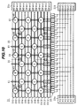
- Fig. 9 illustrates a transfer state of signal charges when they are read from all pixels of the solid state image pickup device having the pixel-shift layout.
- charge signals disposed in one row in the order of R, G, R, G,... are transferred in parallel in the vertical charge transfer paths 35.
- charge signals transferred from photoelectric conversion elements of k columns adjacent in the horizontal direction to the horizontal charge transfer path are to be added and read, the charge signals in the horizontal charge transfer path are driven by a 2k-phase drive method.
- Fig. 10 illustrates a control method for a solid state image pickup device according to a modification of the fourth embodiment.
- the solid state image pickup device shown in Fig. 10 has the structure similar to that shown in Fig. 9.
- a pulse signal ⁇ v2 takes a high positive voltage, e.g., 15 V.
- Signal charges in the B and R photoelectric conversion elements 33 are read to the vertical charge transfer paths 35.
- Signal charges in the vertical charge transfer paths 35 are transferred by a four-phase drive method toward the horizontal charge transfer path by applying pulse signals Fv1 to Fv4 to the vertical charge transfer electrodes.
- the positions of read gates 40 are different for the same color photoelectric conversion elements.
- the read pulse signal ⁇ v2 when the read pulse signal ⁇ v2 is applied, signal charges are read only from specific R and B photoelectric conversion elements in the same row.
- the read gates 40 are positioned either on the EVI or EV2 electrode side corresponding to the pulse signals ⁇ v1 and ⁇ v2. Similarly, in other rows, the positions of read gates 40 are different for the same color photoelectric conversion elements. In this manner, a thinning operation in the horizontal direction is possible.
- signal charges can be read from the photoelectric conversion elements of one column per three columns by applying the read pulses to the charge transfer electrodes.
- the number n of the 1/n horizontal thinning can be changed flexibly.
- the number n of the 1/n horizontal thinning can be changed depending upon to which vertical charge transfer electrode or electrodes the read pulse is applied.
- control gates are provided between the vertical charge transfer paths and horizontal charge transfer path, the number n of the 1/n horizontal thinning can be changed flexibly. Specifically, the control gates select desired vertical charge transfer paths and signal charges are read only from the selected vertical charge transfer paths. This method is disclosed in US Patent Application filed on June 7, 2000, the Case Docket No. P107317-00006.
- the 1/k horizontal thinning is executed by selectively reading signal charges from photoelectric conversion elements of one column per four columns adjacent in the horizontal direction, and then signal charges in the horizontal charge transfer path are driven by the 2k-phase drive method.
- the horizontal charge transfer path 37 is driven by the six-phase drive method.
- the six-phase drive method As the six-phase drive method is used, signal charges transferred from vertical charge transfer paths of one column per three columns can be transferred in the horizontal charge transfer path without an empty signal charge transfer.
- signal charges thinned by 1/3 in the horizontal direction can be output.
- thinned signal charges are output in the order of R, G, B, G,....
- This solid state image pickup device can be used effectively for displaying a clear moving monitor image on a digital still camera.
- a solid state image pickup device according to the fifth embodiment of the invention will be described with reference to Figs. 11 to 14.
- pulse signals ⁇ 1 to ⁇ 4 are applied to pairs of horizontal charge transfer electrodes EH.
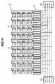
- Fig. 11 illustrates an operation of reading all pixels.
- Photoelectric conversion elements 33 have an RGB vertical stripe color filter layout regularly disposing R, G and B photoelectric conversion elements in a vertical direction.
- Fig. 12 shows the waveforms of drive pulses used for two-phase driving the horizontal charge transfer path 37.
- the drive pulses ⁇ 1 and ⁇ 3 have the same waveform, and the drive pulses ⁇ 2 and ⁇ 4 have the same waveform. Similar to a charge transfer in a horizontal charge transfer path by the two-phase drive method, signal charges can be read from all photoelectric conversion elements.
- the solid state image pickup device shown in Fig. 13 has the same structure as that shown in Fig. 11.
- Fig. 13 shows the distribution of image signals when a 1/2 vertical and horizontal thinning read operations are executed. Also by the 1/2 horizontal thinning read method, an RGB stripe signal is output.
- Fig. 14 shows the waveforms of drive pulses applied to the horizontal charge transfer electrodes EH for the 1/2 vertical and horizontal thinning read operations.
- the pulse signals ⁇ 1 to ⁇ 4 rise from the low level to the high level in the sequential order of ⁇ 1 to ⁇ 4 and fall from the high level to the low level in this order.
- the 1/2 horizontal thinning operation can be executed without an empty charge transfer.
- the power consumption is reduced by 1/2.
- the shape of a pixel may be a square, a polygon or the like in addition to the regular hexagon.
Landscapes
- Engineering & Computer Science (AREA)
- Multimedia (AREA)
- Signal Processing (AREA)
- Solid State Image Pick-Up Elements (AREA)
- Transforming Light Signals Into Electric Signals (AREA)
Abstract
Description
Claims (9)
- A charge transfer device comprising:a semiconductor substrate (1);a charge transfer path formed in said semiconductor substrate and made of a first conductivity type semiconductor layer (7);a plurality of charge transfer electrodes (21) formed close to and above said charge transfer path; anda pulse signal generator circuit (25) for applying either a first pulse signal train for n-phase (n being an integer larger than 1) driving of charges in said charge transfer path to said charge transfer electrodes or a second pulse signal train for (n + 1)-phase or for (n x m) -phase (m being an integer larger than 1) driving of charges in said charge transfer path to said charge transfer electrodes.
- A charge transfer device according to claim 1, said charge transfer path (7) having first barrier layers having a high potential and second well layers having a low potential, disposed alternately; and whereinsaid plurality of charge transfer electrodes comprises a plurality of first and second charge transfer electrodes alternately formed near above the first barrier layers and first well layers of said charge transfer path;a plurality of charge transfer electrode pairs each having adjacent first and second two charge transfer electrodes connected together; andsaid pulse signal generator circuit applying either a pulse signal train of two-phase for 2-phase driving of charges in said charge transfer path to two charge transfer electrode pairs or a pulse signal train for 2k-phase driving or more of charges in said charge transfer path to the charge transfer electrode pairs.
- A charge transfer device according to claim 1 or 2, further comprising:a charge storage region formed adjacent to a final stage of the charge transfer electrodes for temporarily storing charges transferred in said charge transfer path; anda charge detecting region for detecting an amount of charges stored in said charge storage region.
- A charge transfer device according to claim 3 when dependent on claim 2, wherein said charge storage region comprises:a second barrier layer and a second well layer formed adjacent to each other in said charge transfer path;a third charge transfer electrode and a fourth charge transfer electrode formed above the second barrier layer and the second well layer; anda stored charge output pulse generator circuit connected to said third charge transfer electrode and said fourth charge transfer electrode, for generating a stored charge output pulse.
- A charge transfer device according to claim 4, wherein the second well layer has an electric capacity larger than an electric capacity of the first well layer and the channel transfer device further comprises a floating diffusion region formed adjacent to the second well layer for detecting an amount of charges transferred from said charge transfer path.
- A solid state image pickup device comprising a charge transfer device as claimed in any preceding claim, a plurality of photoelectric conversion elements (103) regularly disposed in row and column directions on the semiconductor substrate; a plurality of vertical charge transfer paths extending in a vertical direction and each disposed adjacent to each of a plurality of photoelectric conversion element columns regularly disposed in the column direction; a read gate formed between each photoelectric conversion element and a corresponding vertical charge transfer path for transferring charges accumulated in the photoelectric conversion element to the vertical charge transfer path; a horizontal charge transfer path formed at one ends of the plurality of vertical charge transfer paths for transferring charges in a horizontal direction; and an output amplifier for amplifying charges transferred by the horizontal charge transfer path and outputting the amplified charges.
- A method of reading a solid state image pickup device as claimed in claim 6, the method comprising:either a step of, when charges accumulated in all photoelectric conversion elements are read, transferring charges in the horizontal charge transfer path by a two-phase drive method; ora step of executing a 1/k horizontal thinning operation by selectively reading charges from photoelectric conversion elements adjacent in the horizontal direction of one column per k columns and transferring charges in the horizontal charge transfer path by a 2k-phase drive method.
- A method of reading a solid state image pickup device as claimed in claim 6, the method comprising:either a step of, when charges accumulated in all photoelectric conversion elements are read, transferring charges in the horizontal charge transfer path by a two-phase drive method; ora step of 2k-phase driving the horizontal charge transfer path when charges of j columns of photoelectric conversion elements are transferred in the horizontal charge transfer path and read through addition.
- A method of reading a solid state image pickup device as claimed in claim 6, with a charge transfer device as claimed in claim 5, the method comprising:a step of transferring charges from the charge storage region to the charge detecting region when charges are stored in the charge storage region (
Applications Claiming Priority (4)
| Application Number | Priority Date | Filing Date | Title |
|---|---|---|---|
| JP28733899 | 1999-10-07 | ||
| JP28733899 | 1999-10-07 | ||
| JP2000287486 | 2000-09-21 | ||
| JP2000287486A JP4342095B2 (en) | 1999-10-07 | 2000-09-21 | Charge transfer device, solid-state imaging device using the same, and control method thereof |
Publications (2)
| Publication Number | Publication Date |
|---|---|
| EP1091567A2 true EP1091567A2 (en) | 2001-04-11 |
| EP1091567A3 EP1091567A3 (en) | 2004-02-04 |
Family
ID=26556679
Family Applications (1)
| Application Number | Title | Priority Date | Filing Date |
|---|---|---|---|
| EP00121321A Ceased EP1091567A3 (en) | 1999-10-07 | 2000-10-09 | Charge transfer device, solid state image pickup device using the same, and control method |
Country Status (4)
| Country | Link |
|---|---|
| US (1) | US7079183B1 (en) |
| EP (1) | EP1091567A3 (en) |
| JP (1) | JP4342095B2 (en) |
| KR (1) | KR100549640B1 (en) |
Cited By (1)
| Publication number | Priority date | Publication date | Assignee | Title |
|---|---|---|---|---|
| EP1339237A3 (en) * | 2002-02-21 | 2006-06-07 | Fuji Photo Film Co., Ltd. | Solid state image pickup device |
Families Citing this family (3)
| Publication number | Priority date | Publication date | Assignee | Title |
|---|---|---|---|---|
| JP4049142B2 (en) * | 2004-10-07 | 2008-02-20 | コニカミノルタオプト株式会社 | IMAGING DEVICE, IMAGING ELEMENT DRIVE DEVICE, AND IMAGING METHOD |
| US7965326B2 (en) * | 2006-09-27 | 2011-06-21 | Fujifilm Corporation | Semiconductor element, method of driving semiconductor element and solid imaging apparatus |
| US8687174B2 (en) * | 2010-08-11 | 2014-04-01 | Samsung Electronics Co., Ltd. | Unit pixel, photo-detection device and method of measuring a distance using the same |
Family Cites Families (10)
| Publication number | Priority date | Publication date | Assignee | Title |
|---|---|---|---|---|
| US5317455A (en) * | 1982-07-07 | 1994-05-31 | Canon Kabushiki Kaisha | Recording system which can record signals from two fields for the composition of one picture |
| BE1008077A3 (en) | 1994-02-17 | 1996-01-09 | Philips Electronics Nv | A charge-coupled image sensor arrangement AND CAMERA provided with such a charge-coupled image sensor device. |
| JP3511772B2 (en) * | 1995-12-21 | 2004-03-29 | ソニー株式会社 | Solid-state imaging device, driving method of solid-state imaging device, camera device and camera system |
| JP3800673B2 (en) * | 1996-06-24 | 2006-07-26 | ソニー株式会社 | Solid-state imaging device and driving method thereof |
| US6452634B1 (en) * | 1996-12-26 | 2002-09-17 | Sony Corporation | Charge transfer device and method of driving the same, and solid state imaging device and method of driving the same |
| JP4161384B2 (en) | 1997-04-30 | 2008-10-08 | ソニー株式会社 | Solid-state imaging device, camera using the same, and driving method of solid-state imaging device |
| JP3988207B2 (en) * | 1997-06-02 | 2007-10-10 | ソニー株式会社 | Solid-state imaging device and imaging method thereof |
| JP3262216B2 (en) | 1997-10-15 | 2002-03-04 | 日本電気株式会社 | Solid-state imaging device and driving method thereof |
| JPH11164206A (en) | 1997-12-01 | 1999-06-18 | Fuji Film Microdevices Co Ltd | Solid-state imaging device and charge transfer method |
| JP4131052B2 (en) * | 1998-07-17 | 2008-08-13 | ソニー株式会社 | Imaging device |
-
2000
- 2000-09-21 JP JP2000287486A patent/JP4342095B2/en not_active Expired - Fee Related
- 2000-10-05 KR KR1020000058470A patent/KR100549640B1/en not_active Expired - Fee Related
- 2000-10-06 US US09/680,963 patent/US7079183B1/en not_active Expired - Fee Related
- 2000-10-09 EP EP00121321A patent/EP1091567A3/en not_active Ceased
Cited By (2)
| Publication number | Priority date | Publication date | Assignee | Title |
|---|---|---|---|---|
| EP1339237A3 (en) * | 2002-02-21 | 2006-06-07 | Fuji Photo Film Co., Ltd. | Solid state image pickup device |
| US7202896B2 (en) | 2002-02-21 | 2007-04-10 | Fuji Photo Film Co., Ltd. | Solid state image pickup device having spectral device |
Also Published As
| Publication number | Publication date |
|---|---|
| KR100549640B1 (en) | 2006-02-06 |
| US7079183B1 (en) | 2006-07-18 |
| JP2001177766A (en) | 2001-06-29 |
| EP1091567A3 (en) | 2004-02-04 |
| KR20010050863A (en) | 2001-06-25 |
| JP4342095B2 (en) | 2009-10-14 |
Similar Documents
| Publication | Publication Date | Title |
|---|---|---|
| JPH01106676A (en) | Solid-state image sensor | |
| US7196303B2 (en) | CCD image sensor | |
| US7733398B2 (en) | Photoelectric converting film stack type solid-state image pickup device | |
| JP2983401B2 (en) | Charge transfer method, charge transfer device, and solid-state imaging device using the same | |
| EP1091567A2 (en) | Charge transfer device, solid state image pickup device using the same, and control method | |
| US8803058B2 (en) | Multiple clocking modes for a CCD imager | |
| US8735794B2 (en) | Multiple clocking modes for a CCD imager | |
| US20030038890A1 (en) | Solid state image pickup apparatus of low power consumption and its driving method | |
| US7052929B2 (en) | Solid state image pickup device capable of suppressing smear | |
| US8830372B2 (en) | CCD image sensor having multiple clocking modes | |
| US8723098B2 (en) | Charge coupled image sensor and method of operating with transferring operation of charge packets from plural photodetectors to vertical CCD shift registers (as amended) | |
| US7804539B2 (en) | Solid-state imaging device and method of driving same | |
| JP3718103B2 (en) | Solid-state imaging device, driving method thereof, and camera using the same | |
| JPH04315473A (en) | Solid-state image pickup element | |
| US5900769A (en) | Two-dimensional CCD having storage cells for withdrawing charge packets from transfer channels during horizontal scan periods | |
| JP4148606B2 (en) | Solid-state imaging device and reading method thereof | |
| JP3301176B2 (en) | Charge transfer device | |
| US20060164532A1 (en) | Solid state imaging apparatus and driving method for the solid stateimaging apparatus | |
| US5943095A (en) | Method for operating charge-coupled device at high speed | |
| JP4303950B2 (en) | Method for driving charge transfer device and method for driving solid-state imaging device | |
| US6207982B1 (en) | Solid-state image pickup device capable of high-speed transfer of signal charges in horizontal direction | |
| JP2000196964A (en) | Solid-state imaging device and driving method thereof | |
| JP2739601B2 (en) | Imaging device | |
| JP2768324B2 (en) | Solid-state imaging device and driving method thereof | |
| JP2560984B2 (en) | Imaging unit of charge transfer type solid-state imaging device and driving method thereof |
Legal Events
| Date | Code | Title | Description |
|---|---|---|---|
| PUAI | Public reference made under article 153(3) epc to a published international application that has entered the european phase |
Free format text: ORIGINAL CODE: 0009012 |
|
| AK | Designated contracting states |
Kind code of ref document: A2 Designated state(s): AT BE CH CY DE DK ES FI FR GB GR IE IT LI LU MC NL PT SE |
|
| AX | Request for extension of the european patent |
Free format text: AL;LT;LV;MK;RO;SI |
|
| PUAL | Search report despatched |
Free format text: ORIGINAL CODE: 0009013 |
|
| AK | Designated contracting states |
Kind code of ref document: A3 Designated state(s): AT BE CH CY DE DK ES FI FR GB GR IE IT LI LU MC NL PT SE |
|
| AX | Request for extension of the european patent |
Extension state: AL LT LV MK RO SI |
|
| RIC1 | Information provided on ipc code assigned before grant |
Ipc: 7H 01L 29/768 B Ipc: 7H 01L 27/148 B Ipc: 7H 04N 3/15 A |
|
| 17P | Request for examination filed |
Effective date: 20040225 |
|
| AKX | Designation fees paid |
Designated state(s): DE FR GB |
|
| RAP1 | Party data changed (applicant data changed or rights of an application transferred) |
Owner name: FUJIFILM CORPORATION |
|
| 17Q | First examination report despatched |
Effective date: 20070416 |
|
| STAA | Information on the status of an ep patent application or granted ep patent |
Free format text: STATUS: THE APPLICATION HAS BEEN REFUSED |
|
| 18R | Application refused |
Effective date: 20100219 |