EP1091510A2 - Connection network for high frequency signals - Google Patents
Connection network for high frequency signals Download PDFInfo
- Publication number
- EP1091510A2 EP1091510A2 EP00121680A EP00121680A EP1091510A2 EP 1091510 A2 EP1091510 A2 EP 1091510A2 EP 00121680 A EP00121680 A EP 00121680A EP 00121680 A EP00121680 A EP 00121680A EP 1091510 A2 EP1091510 A2 EP 1091510A2
- Authority
- EP
- European Patent Office
- Prior art keywords
- coupling
- inputs
- outputs
- stage
- switching matrix
- Prior art date
- Legal status (The legal status is an assumption and is not a legal conclusion. Google has not performed a legal analysis and makes no representation as to the accuracy of the status listed.)
- Granted
Links
Images


Classifications
-
- H—ELECTRICITY
- H04—ELECTRIC COMMUNICATION TECHNIQUE
- H04B—TRANSMISSION
- H04B17/00—Monitoring; Testing
- H04B17/30—Monitoring; Testing of propagation channels
- H04B17/391—Modelling the propagation channel
-
- H—ELECTRICITY
- H04—ELECTRIC COMMUNICATION TECHNIQUE
- H04B—TRANSMISSION
- H04B17/00—Monitoring; Testing
- H04B17/20—Monitoring; Testing of receivers
- H04B17/23—Indication means, e.g. displays, alarms, audible means
-
- H—ELECTRICITY
- H04—ELECTRIC COMMUNICATION TECHNIQUE
- H04B—TRANSMISSION
- H04B17/00—Monitoring; Testing
- H04B17/30—Monitoring; Testing of propagation channels
- H04B17/309—Measuring or estimating channel quality parameters
- H04B17/318—Received signal strength
Definitions
- the invention relates to a switching matrix for switching at least one High-frequency signal between at least one transceiver and at least one further transceiver according to the preamble of Claim 1.
- Such a switching matrix represents a radio field simulation, especially for the Mobile radio area and is used for field simulation for the test of Mobile radio equipment, such as transmitters and receivers from mobile radio base stations and mobile terminals.
- the invention has for its object a switching matrix of the aforementioned Art to improve in terms of functionality and manageability.
- the advantage of the invention is that a wide variety of test scenarios can be implemented without a great deal of wiring.
- the necessary coupling modules only have to be connected to one another in the desired manner by means of jumpers or plug connections. A high level of operating convenience is therefore achieved.
- the inputs and outputs of the coupling modules are advantageously routed to connecting sockets arranged on the front and / or rear wall of the housing.
- coupling modules are to be increased provided the switching matrix with another freely interconnectable four-pole hybrid coupler to be equipped with two inputs and two outputs, the Outputs of the second coupling stage via the hybrid coupler with the inputs of the third coupling stage can be connected as desired.
- the step attenuator Semiconductor components exist.
- Semiconductor attenuators also enable one uninterrupted switching, i.e. the signal is not during switching blanked out. This is particularly advantageous when performing series of measurements.
- Another advantage of semiconductor devices is the low level that can be achieved Total insertion loss of typically 17 to 25 dB depending on the connection of the Coupling modules. This means that signals from very weak signal sources can also be used are processed.
- Another preferred embodiment of the invention provides that the Damping values of the step attenuators directly via an attached to the housing Keypad are adjustable and / or can be changed in stages. This contributes to Increase in ease of use.
- the set damping can be displayed directly to the operator.
- the switching matrix is for a frequency range of approx. 800-2500 MHz designed. This large frequency range is made possible by the use of the most modern Semiconductor devices reached. This is the first time a test of dual band or Triband mobile terminals possible in the 900, 1800 and 2200 MHz range work.
- a further development of the invention provides that at the inputs or outputs the first coupling stage signal level display devices are arranged, which in simplest and preferred case an RF coupling element, an RF rectifier and a comparator or threshold circuit with at least one optical Include display element for the signal level. This allows the output to be used the optimal level, which is led to the subsequent coupling stages, simply determine.
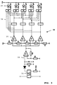
- FIG. 1 is the circuit diagram of a preferred embodiment of the switching matrix shown.
- the switching matrix according to the invention is designed as a passive system, so that bidirectional use is possible, i.e. each described below Signal input can also be a signal output and each described Signal output can be used as a signal input.
- the coupling stage A comprises, for example, four identical coupling modules A1 to A4, the coupling stage B. comprises two identical coupling modules B1, B2 and coupling stage C also two identical coupling modules C1, C2.
- each coupling module A1-A4 there can be a transceiver in it If a base station 1-4 (BTS) of the mobile network is connected.
- the Signal of the base stations 1-4 is in each case by a power divider 5-8 in four Signal branches divided, a signal branch directly to an output, e.g. Bu 1/4 each coupling module A1-A4 is guided.
- the other three signal branches are Signal attenuators 9a-9c, 10a-10c, 11a-11c, 12a-12c downstream, which the Attenuate the signal by 10 dB, 20 dB or 30 dB. Which weaken to different degrees Signals are sent to one output, e.g. Bu 1/1 to Bu 1/3 and so on.
- the coupling modules B1, B2 of the second coupling stage each comprise two inputs Bu 1/5, Bu 2/5 or Bu 3/5, Bu 4/5 and one downstream of each input Step attenuator 13, 14 or 15, 16, which is made up of semiconductor material.
- the Step attenuators have e.g. a control range of 0-63 dB in steps of 1 dB.
- the output signals of the stage attenuators 13, 14 and 15, 16 are over a power divider 17 and 18 merged and are each one Output 5/1 or 6/1 of modules B1, B2 available.
- the regulation of Damping per attenuator is done via a button on the front panel of the Device.
- the coupling modules C1 and C2 of the third coupling stage each include one Four-pole hybrid coupler 19 or 20 with 2 inputs 5/5, 5/3 or 6/5, 6/3 and two exits.
- the outputs of the hybrid couplers 19, 20 are each one Attenuators 21, 22 and 23, 24 on the outputs Bu 7/1, Bu 7/2 and Bu 7/3, Bu 7/4 of the coupling modules C1, C2 performed.
- the reducers have one Attenuation value of 10 dB.
- a further transceiver, e.g. in the form of a mobile terminal 28-31 connected become. There are two for free interconnection with the hybrid couplers 19, 20 Line terminations 26, 27 are provided in the form of 50 ohm loads.
- the switching matrix is free with another one interconnectable four-pole hybrid coupler 25 with two inputs Bu 5/2; Bu 6/2 and two Outputs Bu 5/4; Bu 6/4 equipped.
- FIG. 2 describes an application example of the switching matrix according to the invention, wherein the switching matrix according to Figure 1 for a test connection between one Mobile terminal 28 and four base stations 1-4 is wired. With this The handover behavior of the mobile terminal can be interconnected, for example 28 test.
- the base stations 1-4 are each connected to a coupling module A1-A4, the 10 dB outputs 1/3, 2/3, 3/3 and 4/3 of the coupling modules A1-A4 with the Inputs 1 / 5-4 / 5 of the coupling modules B 1 and B2 are connected.
- the outputs 5/1 and 6/1 of the coupling modules B1 and B2 are connected to the inputs 5/2 and 6/2 Hybrid 25 connected, an output 5/4 to the input 5/3 of the Coupling module C1 is performed.
- Coupling module C2 remains unused. On one Output 7/1 of the coupling module C1, the mobile radio terminal 28 is connected.
- a base station can also be used as a jammer misuse "to simulate interference interference.
- the switching matrix in the first coupling stage for the individual RF paths that described above from User-selectable pre-attenuation in 10 dB steps (0dB, 10dB, 20dB, 30dB), which are used for Adaptation of the entire path damping area is used.
- the user of the RF switching matrix must be aware of the transmission power level of the connected BTSs to control the range of the damping controller of the To be able to optimally use the RF switching matrix. That usually happens when There is a not exactly known RF attenuation between the device under test and the test site is a level measurement of the transmission power level of the connected BTSs Power meters or spectrum analyzers necessary.
- FIG. 3 shows, e.g. in the RF switching matrix to the entrance of everyone Damping paths via a coupler 33 (preferably a 3dB hybrid) that between the respective BTS connection 1-4 and the subsequent power splitter 5-8 is inserted a broadband RF rectifier 34 for power measurement connected.
- the output voltage of this HF rectifier 34 is determined by means of a comparator circuit 35 and a subsequent driver circuit 36 for Control of e.g. LEDs 37 evaluated such that a display by means of LEDs are made in the following way:
- LED 5 (e.g. color red) lights up when the one applied to the RF switching matrix Input power is too high (overload). This is the hint to the user insert an external (additional) attenuator for this path.
- Each of the built-in pre-attenuators e.g. 9a, 9b, 9c or each output Bu 1/1, Bu 1/2, etc.
- an LED in each attenuation path e.g. green
- the lighting of which lights up when the inputs BTSx of the HF Switching matrix with signals below the overdrive limit indicates which output of coupling module Ax is to be connected to the respective input Bu 1/5 - Bu 4/5 of coupling module Bx in order to achieve the optimum dynamic range of the switching matrix.
- LED1 is assigned to pre-attenuation 0dB
- LED2 to pre-attenuation 10dB
- LED4 to pre-attenuation 30dB.
- the switching matrix according to the invention can and is used in a variety of ways very easy to set up for a wide variety of test scenarios.
Landscapes
- Physics & Mathematics (AREA)
- Electromagnetism (AREA)
- Engineering & Computer Science (AREA)
- Computer Networks & Wireless Communication (AREA)
- Signal Processing (AREA)
- Monitoring And Testing Of Transmission In General (AREA)
- Input Circuits Of Receivers And Coupling Of Receivers And Audio Equipment (AREA)
- Use Of Switch Circuits For Exchanges And Methods Of Control Of Multiplex Exchanges (AREA)
- Radio Relay Systems (AREA)
- Transceivers (AREA)
- Control Of Motors That Do Not Use Commutators (AREA)
- Non-Reversible Transmitting Devices (AREA)
Abstract
Description
Die Erfindung betrifft ein Koppelfeld zur Vermittlung wenigstens eines
Hochfrequenzsignals zwischen wenigstens einem Sende-/Empfangsgerät und
wenigstens einem weiteren Sende-/Empfangsgerät nach dem Oberbegriff des
Patentanspruchs 1.The invention relates to a switching matrix for switching at least one
High-frequency signal between at least one transceiver and
at least one further transceiver according to the preamble of
Ein derartiges Koppelfeld stellt eine Funkfeldnachbildung, insbesondere für den Mobilfunkbereich dar und dient zur Feldsimulation für den Test von Mobilfunkequipment, wie Sende- und Empfangsgeräte von Mobilfunk-Basisstationen und Mobilfunkendgeräten.Such a switching matrix represents a radio field simulation, especially for the Mobile radio area and is used for field simulation for the test of Mobile radio equipment, such as transmitters and receivers from mobile radio base stations and mobile terminals.
Bisher wurden Feldsimulationen mit diskret für den jeweiligen Anwendungsfall aufgebauten Koppelfeldern realisiert, wobei insbesondere beim Test von sogenannten Dualband-Mobilfunkendgeräten, die sowohl im GSM (900 MHz) als auch im DCS-Frequenzband (1800 MHz) arbeiten ein hoher Verschaltungsaufwand nötig war. Dabei war die Bedienbarkeit der diskret aufgebauten Koppelfelder wenig benutzerfreundlich. Zur Simulation der Dämpfung der Funksignale wurden als Abschwächer verschaltete Koaxial-Relais verwendet, die einerseits eine gewisse Schaltzeit und andererseits nur eine begrenzte Lebensdauer aufweisen. Ferner ergab sich beim Umschalten von einem Dämpfungswert auf einen anderen eine gewisse Austastzeit des Funksignals, was die Messungen erschwerte.So far, field simulations have been discrete for each application implemented coupling fields, especially when testing So-called dual-band mobile terminals, both in GSM (900 MHz) as In the DCS frequency band (1800 MHz), too, a lot of wiring work was necessary. The usability of the discrete coupling fields was little user friendly. To simulate the attenuation of the radio signals were used as Attenuator interconnected coaxial relays are used, on the one hand a certain Switching time and on the other hand only have a limited life. Furthermore, switching from one damping value to another resulted a certain blanking time of the radio signal, which made the measurements more difficult.
Der Erfindung liegt die Aufgabe zugrunde, ein Koppelfeld der eingangs genannten Art hinsichtlich der Funktionalität und Handhabbarkeit zu verbessern.The invention has for its object a switching matrix of the aforementioned Art to improve in terms of functionality and manageability.
Diese Aufgabe wird erfindungsgemäß durch die im unabhängigen Patentanspruch angegebenen Merkmale gelöst. This object is achieved by the independent claim specified features solved.
Danach umfasst das Koppelfeld eine erste Koppelstufe mit wenigstens zwei
gleichartigen Koppelmodulen zum Anschluß wenigstens eines Sende-/Empfangsgeräts,
wobei die Koppelmodule jeweils einen Leistungsteiler und
wenigstens einen festen oder variablen Signalabschwächer und Ausgänge
aufweisen, an denen das ungedämpfte Eingangssignal und wenigstens ein
abgeschwächtes Eingangssignal zur Verfügung stehen,
wobei die Eingänge der zweiten und dritten Koppelstufe über Steckbrücken und/oder Verbindungskabel mit den Ausgängen der ersten und zweiten Koppelstufe beliebig miteinander verbindbar sind.
the inputs of the second and third coupling stages can be connected to one another as desired with the outputs of the first and second coupling stages via jumpers and / or connecting cables.
Mit der Erfindung wird der Vorteil erreicht, daß verschiedenste Prüfszenarien ohne
großen Verschaltungsaufwand realisiert werden können. Die notwendigen
Koppelmodule müssen lediglich durch Steckbrücken oder Steckverbindungen in
gewünschter Weise miteinander verbunden werden. Es wird demnach ein hoher
Bedienkomfort erreicht. Vorteilhaft sind die Eingänge und Ausgänge der
Koppelmodule auf an der Front- und/oder Rückwand des Gehäuses angeordnete
Verbindungsbuchsen geführt.
Durch Einbau in ein Standardgehäuse, z.B. 19" Gehäuse, lässt sich das Koppelfeld
leicht transportieren und überall einsetzen.The advantage of the invention is that a wide variety of test scenarios can be implemented without a great deal of wiring. The necessary coupling modules only have to be connected to one another in the desired manner by means of jumpers or plug connections. A high level of operating convenience is therefore achieved. The inputs and outputs of the coupling modules are advantageously routed to connecting sockets arranged on the front and / or rear wall of the housing.
By installing in a standard housing, eg 19 "housing, the switching matrix can be easily transported and used anywhere.
Um die Verschaltungs- und Kombinationsmöglichkeiten zwischen den Koppelmodulen zu erhöhen ist in einer bevorzugten Ausführungsform der Erfindung vorgesehen, das Koppelfeld mit einem weiteren frei verschaltbaren Vierpol-Hybridkoppler mit zwei Eingängen und zwei Ausgängen auszurüsten, wobei die Ausgänge der zweiten Koppelstufe über den Hybridkoppler mit den Eingängen der dritten Koppelstufe beliebig verbindbar sind.To the interconnection and combination options between the In a preferred embodiment of the invention, coupling modules are to be increased provided the switching matrix with another freely interconnectable four-pole hybrid coupler to be equipped with two inputs and two outputs, the Outputs of the second coupling stage via the hybrid coupler with the inputs of the third coupling stage can be connected as desired.
Kurze Schaltzeiten der Stufenabschwächer sowie eine lange Lebensdauer im Vergleich zu Relaisschaltstufen lassen sich gemäß einer Ausführungsform der Erfindung dadurch erzielen, daß der Stufenabschwächer aus Haibleiterbauelementen besteht. Halbleiterabschwächer ermöglichen außerdem ein unterbrechungsfreies Schalten, d.h. das Signal wird während des Schaltens nicht ausgetastet. Dies ist insbesondere bei der Durchführung von Meßreihen vorteilhaft. Ein weiterer Vorteil von Halbleiterbausteinen ist die dadurch erzielbare geringe Gesamt-Einfügedämpfung von typisch 17 bis 25 dB je nach Verschaltung der Koppelmodule. Somit können auch Signale von sehr schwachen Signalquellen verarbeitet werden.Short switching times of the step attenuators and a long service life in the According to an embodiment of the Achieve invention in that the step attenuator Semiconductor components exist. Semiconductor attenuators also enable one uninterrupted switching, i.e. the signal is not during switching blanked out. This is particularly advantageous when performing series of measurements. Another advantage of semiconductor devices is the low level that can be achieved Total insertion loss of typically 17 to 25 dB depending on the connection of the Coupling modules. This means that signals from very weak signal sources can also be used are processed.
Eine weitere bevorzugte Ausführungsform der Erfindung sieht vor, daß die Dämpfungswerte der Stufenabschwächer direkt über ein am Gehäuse angebrachtes Tastenfeld einstellbar und/oder stufenweise veränderbar sind. Dies trägt zur Erhöhung des Bedienkomforts bei. Durch eine entsprechende Anzeigevorrichtung kann die eingestellte Dämpfung dem Bediener direkt angezeigt werden.Another preferred embodiment of the invention provides that the Damping values of the step attenuators directly via an attached to the housing Keypad are adjustable and / or can be changed in stages. This contributes to Increase in ease of use. By a corresponding display device the set damping can be displayed directly to the operator.
Erfindungsgemäß ist das Koppelfeld für einen Frequenzbereich von ca. 800-2500 MHz ausgelegt. Dieser große Frequenzbereich wird durch den Einsatz modernster Halbleiterbauelemete erreicht. Dadurch wird erstmals ein Test von Dualband- oder Triband-Mobilfunkendgeräten möglich, die im 900, 1800 bzw. 2200 MHz Bereich arbeiten.According to the invention, the switching matrix is for a frequency range of approx. 800-2500 MHz designed. This large frequency range is made possible by the use of the most modern Semiconductor devices reached. This is the first time a test of dual band or Triband mobile terminals possible in the 900, 1800 and 2200 MHz range work.
Eine Weiterbildung der Erfindung sieht vor, daß an den Eingängen oder Ausgängen der ersten Koppelstufe Signalpegelanzeigeeinrichtungen angeordnet sind, die im einfachsten und bevorzugten Fall ein HF-Koppelglied, einen HF-Gleichrichter und eine Komparator- oder Schwellwertschaltung mit wenigstens einem optischem Anzeigeelement für den Signalpegel umfassen. Dadurch lässt sich der Ausgang mit dem optimalen Pegel, der auf die nachfolgenden Koppelstufen geführt wird, einfach bestimmen.A further development of the invention provides that at the inputs or outputs the first coupling stage signal level display devices are arranged, which in simplest and preferred case an RF coupling element, an RF rectifier and a comparator or threshold circuit with at least one optical Include display element for the signal level. This allows the output to be used the optimal level, which is led to the subsequent coupling stages, simply determine.
Nachfolgend wird die Erfindung anhand eines Ausführungsbeispiels unter Bezugnahme auf zwei Zeichnungsfiguren näher beschrieben. Dabei gehen aus den Zeichnungen und ihrer Beschreibung weitere Merkmale und Vorteile der Erfindung hervor. Es zeigen:
- Figur 1:
- das Schaltbild einer bevorzugten Ausführung des Koppelfelds;
- Figur 2:
- Zusammenschaltung der Koppelmodule für eine Testverbindung zwischen einem Mobilfunkendgerät und vier Basisstationen;
- Figur 3:
- Schaltungsanordnung zur Signalpegelauswertung.
- Figure 1:
- the circuit diagram of a preferred embodiment of the switching matrix;
- Figure 2:
- Interconnection of the coupling modules for a test connection between a mobile radio terminal and four base stations;
- Figure 3:
- Circuit arrangement for signal level evaluation.
In Figur 1 ist das Schaltbild einer bevorzugten Ausführung des Koppelfelds dargestellt. Das erfindungsgemäße Koppelfeld ist als passives System ausgeführt, so daß eine bidirektionale Nutzung möglich ist, d.h. jeder im folgenden beschriebene Signaleingang kann auch ein Signalausgang sein und jeder beschriebene Signalausgang als Signaleingang verwendet werden.In Figure 1 is the circuit diagram of a preferred embodiment of the switching matrix shown. The switching matrix according to the invention is designed as a passive system, so that bidirectional use is possible, i.e. each described below Signal input can also be a signal output and each described Signal output can be used as a signal input.
Man erkennt die drei wesentlichen Koppelstufen A, B und C. Die Koppelstufe A umfasst beispielsweise vier identische Koppelmodule A1 bis A4, die Koppelstufe B umfasst zwei identische Koppelmodule B1, B2 und die Koppelstufe C ebenfalls zwei identische Koppelmodule C1, C2.One recognizes the three essential coupling stages A, B and C. The coupling stage A comprises, for example, four identical coupling modules A1 to A4, the coupling stage B. comprises two identical coupling modules B1, B2 and coupling stage C also two identical coupling modules C1, C2.
Am Eingang jedes Koppelmoduls A1-A4 kann ein Sende-/Empfangsgerät, in diesem
Fall eine Basisstation 1-4 (BTS) des Mobilfunknetzes, angeschlossen werden. Das
Signal der Basisstationen 1-4 wird jeweils von einem Leistungsteiler 5-8 in vier
Signalzweige geteilt, wobei ein Signalzweig direkt an einen Ausgang, z.B. Bu 1/4
jedes Koppelmoduls A1-A4 geführt wird. Den anderen drei Signalzweigen werden
Signalabschwächer 9a-9c, 10a-10c, 11a-11c, 12a-12c nachgeschaltet, die das
Signal um 10 dB, 20 dB oder 30 dB dämpfen. Die verschieden stark abschwächten
Signale werden an jeweils einen Ausgang, z.B. Bu 1/1 bis Bu 1/3 usw. geführt. At the input of each coupling module A1-A4 there can be a transceiver in it
If a base station 1-4 (BTS) of the mobile network is connected. The
Signal of the base stations 1-4 is in each case by a power divider 5-8 in four
Signal branches divided, a signal branch directly to an output,
Die Koppelmodule B1, B2 der zweiten Koppelstufe umfassen jeweils zwei Eingänge
Bu 1/5, Bu 2/5 bzw. Bu 3/5, Bu 4/5 und einen jedem Eingang nachgeschalteten
Stufenabschwächer 13, 14 bzw. 15, 16, der aus Halbleitermaterial aufgebaut ist. Die
Stufenabschwächer haben z.B. einen Regelbereich von 0-63 dB in Schritten von 1
dB. Die Ausgangssignale der Stufenabschwächer 13, 14 bzw. 15, 16 werden über
einen Leistungsteiler 17 bzw. 18 zusammengeführt und stehen an jeweils einem
Ausgang 5/1 bzw. 6/1 der Module B1, B2 zur Verfügung. Die Regelung der
Dämpfung pro Abschwächer erfolgt über ein Tastenteld auf der Frontplatte des
Geräts.The coupling modules B1, B2 of the second coupling stage each comprise two
Die Koppelmodule C1 und C2 der dritten Koppelstufe umfassen jeweils einen
Vierpol-Hybridkoppler 19 bzw. 20 mit jeweils 2 Eingängen 5/5, 5/3 bzw. 6/5, 6/3 und
zwei Ausgängen. Die Ausgänge der Hybridkoppler 19, 20 werden über jeweils einen
Abschwächer 21, 22 bzw. 23, 24 an die Ausgänge Bu 7/1, Bu 7/2 bzw. Bu 7/3, Bu
7/4 der Koppelmodule C1, C2 geführt. Die Abschwächer haben beispielsweise einen
Dämpfungswert von 10 dB. An jedem Ausgang kann ein weiteres Sende-/Empfangsgerät,
z.B. in Form eines Mobilfunkendgeräts 28-31, angeschlossen
werden. Zur freien Verschaltung mit den Hybridkopplern 19, 20 sind zwei
Leitungsabschlüsse 26, 27 in Form von 50 Ohm Lasten vorgesehen.The coupling modules C1 and C2 of the third coupling stage each include one
Four-
Um die Verschaltungs- und Kombinationsmöglichkeiten zwischen den
Koppelmodulen 6 und C zu erhöhen ist das Koppelfeld mit einem weiteren frei
verschaltbaren Vierpol-Hybridkoppler 25 mit zwei Eingängen Bu 5/2; Bu 6/2 und zwei
Ausgängen Bu 5/4; Bu 6/4 ausgerüstet.To the interconnection and combination options between the
To increase
Figur 2 beschreibt ein Anwendungsbeispiel des erfindungsgemäßen Koppelfeldes,
wobei das Koppelfeld gemäß Figur 1 für eine Testverbindung zwischen einem
Mobilfunkendgerät 28 und vier Basisstationen 1-4 verdrahtet ist. Mit dieser
Verschaltung lässt sich zum Beispiel das Handoververhalten des Mobilfunkendgeräts
28 testen. FIG. 2 describes an application example of the switching matrix according to the invention,
wherein the switching matrix according to Figure 1 for a test connection between one
Die Basisstationen 1-4 sind an jeweils einem Koppelmodul A1-A4 angeschlossen,
wobei die 10 dB Ausgänge 1/3, 2/3, 3/3 und 4/3 der Koppelmodule A1-A4 mit den
Eingängen 1/5-4/5 der Koppelmodule B 1 und B2 verbunden sind. Die Ausgänge 5/1
und 6/1 der Koppelmodule B1 und B2 sind mit den Eingängen 5/2 und 6/2 des
Hybrids 25 verbunden, dessen einer Ausgang 5/4 auf den Eingang 5/3 des
Koppelmoduls C1 geführt wird. Koppelmodul C2 bleibt unbenutzt. An einem
Ausgang 7/1 des Koppelmoduls C1 ist das Mobilfunkendgerät 28 angeschlossen.The base stations 1-4 are each connected to a coupling module A1-A4,
the 10
Durch Verändern der Signalpegel der Basisstationen 1-4 mit Hilfe der
Stufenabschwächer 13-16 der Koppelstufen B1 und B2 lässt sich eine Bewegung
des Mobilfunkendgeräts 28, d.h. eine Änderung der Entfernung zu den
Basisstationen 1-4, simulieren und so das Handoververhalten des
Mobilfunkendgerätes 28 testen. Ferner lässt sich z.B. eine Basisstation als
Störsender ![]()
![]()
Um die erforderliche Meßdynamik günstig zu realisieren, beinhaltet das Koppelfeld in der ersten Koppelstufe für die einzelnen HF-Pfade die oben beschriebene vom Benutzer wählbare Vordämpfung in 10 dB-Stufen (0dB, 10dB, 20dB, 30dB), die zur Anpassung des gesamten Pfaddämpfungsbereiches dient. In dieser Ausführung muß der Benutzer des HF-Koppelfeldes Kenntnis über die Sendeleistungspegel der angeschlossenen BTSn besitzen, um den Regel-bereich der Dämpfungssteller des HF-Koppelfeldes optimal nutzen zu können. Das macht im Normalfall, wenn zwischen Prüfling und Testort eine nicht genau bekannte HF-Dämpfung vorhanden ist, eine Pegelmessung der Sendeleistungspegel der angeschlossenen BTSn mit Hilfe von Power-Metern oder Spektrumsanalysatoren notwendig.In order to implement the required measurement dynamics cheaply, the switching matrix in the first coupling stage for the individual RF paths that described above from User-selectable pre-attenuation in 10 dB steps (0dB, 10dB, 20dB, 30dB), which are used for Adaptation of the entire path damping area is used. In this version the user of the RF switching matrix must be aware of the transmission power level of the connected BTSs to control the range of the damping controller of the To be able to optimally use the RF switching matrix. That usually happens when There is a not exactly known RF attenuation between the device under test and the test site is a level measurement of the transmission power level of the connected BTSs Power meters or spectrum analyzers necessary.
In einer Weiterbildung der Erfindung gemäß Figur 1 und insbesondere Figur 3 ist nun
vorgesehen, daß jeweils eine Signalpegelanzeigeeinnchtung 32 in die
Signalleitungen zwischen den Basisstationen 1-4 und den Leistungsteilern 5-8
geschaltet ist. Genauso gut könnten die Signalpegeleinrichtungen 32 an den
ungedämpften Ausgängen Bu 1/4, Bu 2/4 usw. der ersten Koppelstufe angeordnet
werden. In a development of the invention according to Figure 1 and in particular Figure 3 is now
provided that a
Mit Hilfe dieser Singalpegelanzeigeeinrichtungen 32 wird dem Benutzer des HF-Koppelfeldes
auf einfache und ökonomisch günstige Art einen Hinweis über die
optimale einzustellende Vordämpfung der einzelnen Dämpfungspfade gegeben.With the help of these singal
Wie Figur 3 zeigt, wird im HF-Koppelfeld z.B. an den Eingang eines jeden
Dämpfungspfades über einen Koppler 33 (vorzugsweise ein 3dB-Hybrid), der
zwischen dem jeweiligen BTS-Anschluß 1-4 und dem nachfolgenden Power-Splitter
5-8 eingefügt wird ein breitbandiger HF-Gleichrichter 34 zur Leistungsmessung
angeschlossen. Die Ausgangsspannung dieses HF-Gleichrichters 34 wird mittels
einer Komparatorschaltung 35 und einer nachfolgenden Treiberschaltung 36 zur
Ansteuerung von z.B. LEDs 37 derart ausgewertet, daß eine Anzeige mittels der
LEDs in der folgenden Art erfolgt :As FIG. 3 shows, e.g. in the RF switching matrix to the entrance of everyone
Damping paths via a coupler 33 (preferably a 3dB hybrid) that
between the respective BTS connection 1-4 and the subsequent power splitter
5-8 is inserted a
LED 5 (z.B. Farbe rot) leuchtet, wenn die am HF-Koppelfeld angelegte Eingangsleistung zu hoch ist (Übersteuerung). Das ist der Hinweis für den Benutzer, für diesen Pfad ein externes (Zusatz)-Dämpfungsglied einzufügen.LED 5 (e.g. color red) lights up when the one applied to the RF switching matrix Input power is too high (overload). This is the hint to the user insert an external (additional) attenuator for this path.
Jedem der eingebauten Vordämpfungsglieder z.B. 9a, 9b, 9c bzw. jedem Ausgang
Bu 1/1, Bu 1/2, usw. wird in jedem Dämpfungspfad eine LED zugeordnet (z.B. grün),
deren Aufleuchten dem Benutzer bei Ansteuerung der Eingänge BTSx des HF-Koppelfeldes
mit Signalen unterhalb der Übersteuerungsgrenze anzeigt, welcher
Ausgang der Koppelmodule Ax mit dem jeweiligen Eingang Bu 1/5 - Bu 4/5 der
Koppelmodule Bx zu verbinden sind, um den optimalen Dynamikbereich des
Koppelfeldes zu erzielen.
Hierbei wird LED1 der Vordämpfung 0dB, LED2 der Vordämpfung 10dB, LED3 der
Vordämpfung 20dB und LED4 der Vordämpfung 30dB zugeordnet.Each of the built-in pre-attenuators, e.g. 9a, 9b, 9c or each
LED1 is assigned to pre-attenuation 0dB, LED2 to pre-attenuation 10dB, LED3 to pre-attenuation 20dB and LED4 to pre-attenuation 30dB.
Das erfindungsgemäße Koppelfeld lässt sich auf vielfältige Weise einsetzen und ist dabei sehr einfach auf verschiedenste Testszenarien einzurichten. The switching matrix according to the invention can and is used in a variety of ways very easy to set up for a wide variety of test scenarios.
- AA
- KoppelstufeCoupling stage
- A1A1
- KoppelmodulCoupling module
- A2A2
- KoppelmodulCoupling module
- A3A3
- KoppelmodulCoupling module
- A4A4
- KoppelmodulCoupling module
- BB
- KoppelstufeCoupling stage
- B1B1
- KoppelmodulCoupling module
- B2B2
- KoppelmodulCoupling module
- CC.
- KoppelstufeCoupling stage
- C1C1
- KoppelmodulCoupling module
- C2C2
- KoppelmodulCoupling module
- 1-41-4
- Sende-/EmpfangsgerätTransceiver
- 5-85-8
- LeistungsteilerPower divider
- 9-129-12
- AbschwächerReducer
- 13-1613-16
- Abschwächer variabelReducer variable
- 17,1817.18
- LeistungsteilerPower divider
- 19,2019.20
- HybndkopplerHybrid coupler
- 21-2421-24
- AbschwächerReducer
- 2525th
- HybridkopplerHybrid coupler
- 26,2726.27
- LeitungsabschlußLine termination
- 28-3128-31
- Sende-/EmpfangsgerätTransceiver
- 3232
- SignalpegelanzeigeeinrichtungSignal level indicator
- 3333
- HF-KopplerRF coupler
- 3434
- HF-GleichrichterRF rectifier
- 3535
- KomparatorschaltungComparator circuit
- 3636
- TreiberschaltungDriver circuit
- 3737
- LEDsLEDs
Claims (11)
wobei die Eingänge der zweiten und dritten Koppelstufe (B; C) über Steckbrücken und/oder Verbindungskabel mit den Ausgängen der ersten und zweiten Koppelstufe (A; B) beliebig miteinander verbindbar sind.
the inputs of the second and third coupling stages (B; C) can be connected to one another as desired with the outputs of the first and second coupling stages (A; B) by means of jumpers and / or connecting cables.
Applications Claiming Priority (2)
| Application Number | Priority Date | Filing Date | Title |
|---|---|---|---|
| DE19947654 | 1999-10-04 | ||
| DE19947654A DE19947654A1 (en) | 1999-10-04 | 1999-10-04 | Header field for high frequency signals |
Publications (3)
| Publication Number | Publication Date |
|---|---|
| EP1091510A2 true EP1091510A2 (en) | 2001-04-11 |
| EP1091510A3 EP1091510A3 (en) | 2003-09-03 |
| EP1091510B1 EP1091510B1 (en) | 2005-05-25 |
Family
ID=7924367
Family Applications (1)
| Application Number | Title | Priority Date | Filing Date |
|---|---|---|---|
| EP00121680A Expired - Lifetime EP1091510B1 (en) | 1999-10-04 | 2000-10-04 | Connection network for high frequency signals |
Country Status (4)
| Country | Link |
|---|---|
| US (1) | US6804200B1 (en) |
| EP (1) | EP1091510B1 (en) |
| AT (1) | ATE296508T1 (en) |
| DE (2) | DE19947654A1 (en) |
Cited By (1)
| Publication number | Priority date | Publication date | Assignee | Title |
|---|---|---|---|---|
| WO2005057972A1 (en) * | 2003-12-12 | 2005-06-23 | Willtek Communications Gmbh | Method and device for testing mobile phones |
Families Citing this family (2)
| Publication number | Priority date | Publication date | Assignee | Title |
|---|---|---|---|---|
| KR101915526B1 (en) * | 2012-04-17 | 2018-11-06 | 삼성전자 주식회사 | Antenna apparatus of portable terminal |
| US8902902B2 (en) | 2012-07-18 | 2014-12-02 | Netronome Systems, Incorporated | Recursive lookup with a hardware trie structure that has no sequential logic elements |
Citations (3)
| Publication number | Priority date | Publication date | Assignee | Title |
|---|---|---|---|---|
| US5191594A (en) * | 1991-11-27 | 1993-03-02 | The United States Of America As Represented By The United States Department Of Energy | Fading channel simulator |
| US5465393A (en) * | 1993-04-12 | 1995-11-07 | Telefonaktiebolaget Lm Ericsson | Simulated air interface system for simulating radio communication |
| US5862455A (en) * | 1993-06-07 | 1999-01-19 | Martin Communications Pty Ltd | Fading simulator |
Family Cites Families (3)
| Publication number | Priority date | Publication date | Assignee | Title |
|---|---|---|---|---|
| KR100202502B1 (en) * | 1996-12-30 | 1999-06-15 | 정장호 | Circuit for testing base station in mobile communication system |
| KR100268231B1 (en) * | 1998-05-30 | 2000-10-16 | 윤종용 | An apparatus and method for air interface simulation |
| JP3516663B2 (en) * | 2001-02-26 | 2004-04-05 | 埼玉日本電気株式会社 | CDMA base station test apparatus and base station test method |
-
1999
- 1999-10-04 DE DE19947654A patent/DE19947654A1/en not_active Withdrawn
-
2000
- 2000-10-04 US US09/679,655 patent/US6804200B1/en not_active Expired - Lifetime
- 2000-10-04 AT AT00121680T patent/ATE296508T1/en active
- 2000-10-04 DE DE50010382T patent/DE50010382D1/en not_active Expired - Lifetime
- 2000-10-04 EP EP00121680A patent/EP1091510B1/en not_active Expired - Lifetime
Patent Citations (3)
| Publication number | Priority date | Publication date | Assignee | Title |
|---|---|---|---|---|
| US5191594A (en) * | 1991-11-27 | 1993-03-02 | The United States Of America As Represented By The United States Department Of Energy | Fading channel simulator |
| US5465393A (en) * | 1993-04-12 | 1995-11-07 | Telefonaktiebolaget Lm Ericsson | Simulated air interface system for simulating radio communication |
| US5862455A (en) * | 1993-06-07 | 1999-01-19 | Martin Communications Pty Ltd | Fading simulator |
Cited By (1)
| Publication number | Priority date | Publication date | Assignee | Title |
|---|---|---|---|---|
| WO2005057972A1 (en) * | 2003-12-12 | 2005-06-23 | Willtek Communications Gmbh | Method and device for testing mobile phones |
Also Published As
| Publication number | Publication date |
|---|---|
| ATE296508T1 (en) | 2005-06-15 |
| EP1091510B1 (en) | 2005-05-25 |
| US6804200B1 (en) | 2004-10-12 |
| DE19947654A1 (en) | 2001-04-12 |
| EP1091510A3 (en) | 2003-09-03 |
| DE50010382D1 (en) | 2005-06-30 |
Similar Documents
| Publication | Publication Date | Title |
|---|---|---|
| DE69532373T2 (en) | Modular connection matrix for the matrical connection of antennas with radio channel units | |
| DE19525430C2 (en) | Circuit network measuring device and method for calibration | |
| DE4327137C2 (en) | Step attenuator | |
| DE10052711A1 (en) | Multiband terminal | |
| DE19528972B4 (en) | Serial digital signal source with a cable loss simulator | |
| EP1091510B1 (en) | Connection network for high frequency signals | |
| WO2005109975A2 (en) | Broadband balance-to-unbalance transformer | |
| EP0810445B1 (en) | Method for the screen effectiveness determination of a part of a shielded cable | |
| EP2294701A1 (en) | Front end module and method for testing a front end module | |
| EP2506563B1 (en) | Switching device | |
| EP0225461B1 (en) | Home signal distributing apparatus | |
| DE102005044620B4 (en) | Front end module for wireless communication | |
| DE102014223883B4 (en) | Multi-channel wireless microphone system | |
| DE4404046C2 (en) | Method for calibrating a network analyzer with two measuring gates | |
| DE60218901T2 (en) | METHOD AND SYSTEM FOR TRANSMITTING CARRYING SIGNALS BETWEEN A FIRST AND A SECOND ANTENNA NETWORK | |
| DE10340619B4 (en) | attenuator | |
| CN108650032A (en) | A kind of test device and method of the Multi-channel signal selecting automatically controlled | |
| EP1649611B1 (en) | Measuring adapter for simulating a low-voltage network that is coupled to a powerline data transmission device | |
| WO2016206980A1 (en) | Device and method for simulating fault conditions in a line | |
| DE102016123474A1 (en) | RF module and method for testing an RF module | |
| EP2947871A2 (en) | High frequency signal switching matrix | |
| DE102005018865B4 (en) | Method and apparatus for measuring using a main and a remote unit | |
| DE10332808B4 (en) | Calibration line arrangement | |
| DE19706334A1 (en) | Logarithmic converter for input circuit of waveform analyser e.g. spectrum analyser | |
| DE102022112463A1 (en) | Device and arrangement for checking the functionality of a charging station |
Legal Events
| Date | Code | Title | Description |
|---|---|---|---|
| PUAI | Public reference made under article 153(3) epc to a published international application that has entered the european phase |
Free format text: ORIGINAL CODE: 0009012 |
|
| AK | Designated contracting states |
Kind code of ref document: A2 Designated state(s): AT BE CH CY DE DK ES FI FR GB GR IE IT LI LU MC NL PT SE |
|
| AX | Request for extension of the european patent |
Free format text: AL;LT;LV;MK;RO;SI |
|
| RAP1 | Party data changed (applicant data changed or rights of an application transferred) |
Owner name: T-MOBILE DEUTSCHLAND GMBH Owner name: MTS SYSTEMTECHNIK GMBH |
|
| PUAL | Search report despatched |
Free format text: ORIGINAL CODE: 0009013 |
|
| AK | Designated contracting states |
Kind code of ref document: A3 Designated state(s): AT BE CH CY DE DK ES FI FR GB GR IE IT LI LU MC NL PT SE |
|
| AX | Request for extension of the european patent |
Extension state: AL LT LV MK RO SI |
|
| 17P | Request for examination filed |
Effective date: 20031029 |
|
| 17Q | First examination report despatched |
Effective date: 20040406 |
|
| AKX | Designation fees paid |
Designated state(s): AT BE CH CY DE DK ES FI FR GB GR IE IT LI LU MC NL PT SE |
|
| GRAP | Despatch of communication of intention to grant a patent |
Free format text: ORIGINAL CODE: EPIDOSNIGR1 |
|
| GRAS | Grant fee paid |
Free format text: ORIGINAL CODE: EPIDOSNIGR3 |
|
| GRAA | (expected) grant |
Free format text: ORIGINAL CODE: 0009210 |
|
| AK | Designated contracting states |
Kind code of ref document: B1 Designated state(s): AT BE CH CY DE DK ES FI FR GB GR IE IT LI LU MC NL PT SE |
|
| PG25 | Lapsed in a contracting state [announced via postgrant information from national office to epo] |
Ref country code: IT Free format text: LAPSE BECAUSE OF FAILURE TO SUBMIT A TRANSLATION OF THE DESCRIPTION OR TO PAY THE FEE WITHIN THE PRESCRIBED TIME-LIMIT;WARNING: LAPSES OF ITALIAN PATENTS WITH EFFECTIVE DATE BEFORE 2007 MAY HAVE OCCURRED AT ANY TIME BEFORE 2007. THE CORRECT EFFECTIVE DATE MAY BE DIFFERENT FROM THE ONE RECORDED. Effective date: 20050525 Ref country code: IE Free format text: LAPSE BECAUSE OF FAILURE TO SUBMIT A TRANSLATION OF THE DESCRIPTION OR TO PAY THE FEE WITHIN THE PRESCRIBED TIME-LIMIT Effective date: 20050525 Ref country code: FI Free format text: LAPSE BECAUSE OF FAILURE TO SUBMIT A TRANSLATION OF THE DESCRIPTION OR TO PAY THE FEE WITHIN THE PRESCRIBED TIME-LIMIT Effective date: 20050525 |
|
| REG | Reference to a national code |
Ref country code: GB Ref legal event code: FG4D Free format text: NOT ENGLISH |
|
| REG | Reference to a national code |
Ref country code: CH Ref legal event code: EP |
|
| REG | Reference to a national code |
Ref country code: IE Ref legal event code: FG4D Free format text: LANGUAGE OF EP DOCUMENT: GERMAN |
|
| REF | Corresponds to: |
Ref document number: 50010382 Country of ref document: DE Date of ref document: 20050630 Kind code of ref document: P |
|
| PG25 | Lapsed in a contracting state [announced via postgrant information from national office to epo] |
Ref country code: DK Free format text: LAPSE BECAUSE OF FAILURE TO SUBMIT A TRANSLATION OF THE DESCRIPTION OR TO PAY THE FEE WITHIN THE PRESCRIBED TIME-LIMIT Effective date: 20050825 Ref country code: GR Free format text: LAPSE BECAUSE OF FAILURE TO SUBMIT A TRANSLATION OF THE DESCRIPTION OR TO PAY THE FEE WITHIN THE PRESCRIBED TIME-LIMIT Effective date: 20050825 Ref country code: SE Free format text: LAPSE BECAUSE OF FAILURE TO SUBMIT A TRANSLATION OF THE DESCRIPTION OR TO PAY THE FEE WITHIN THE PRESCRIBED TIME-LIMIT Effective date: 20050825 |
|
| PG25 | Lapsed in a contracting state [announced via postgrant information from national office to epo] |
Ref country code: ES Free format text: LAPSE BECAUSE OF FAILURE TO SUBMIT A TRANSLATION OF THE DESCRIPTION OR TO PAY THE FEE WITHIN THE PRESCRIBED TIME-LIMIT Effective date: 20050905 |
|
| PG25 | Lapsed in a contracting state [announced via postgrant information from national office to epo] |
Ref country code: CY Free format text: LAPSE BECAUSE OF FAILURE TO SUBMIT A TRANSLATION OF THE DESCRIPTION OR TO PAY THE FEE WITHIN THE PRESCRIBED TIME-LIMIT Effective date: 20051004 |
|
| GBT | Gb: translation of ep patent filed (gb section 77(6)(a)/1977) |
Effective date: 20050919 |
|
| PG25 | Lapsed in a contracting state [announced via postgrant information from national office to epo] |
Ref country code: PT Free format text: LAPSE BECAUSE OF FAILURE TO SUBMIT A TRANSLATION OF THE DESCRIPTION OR TO PAY THE FEE WITHIN THE PRESCRIBED TIME-LIMIT Effective date: 20051027 |
|
| PG25 | Lapsed in a contracting state [announced via postgrant information from national office to epo] |
Ref country code: LI Free format text: LAPSE BECAUSE OF NON-PAYMENT OF DUE FEES Effective date: 20051031 Ref country code: MC Free format text: LAPSE BECAUSE OF NON-PAYMENT OF DUE FEES Effective date: 20051031 Ref country code: LU Free format text: LAPSE BECAUSE OF NON-PAYMENT OF DUE FEES Effective date: 20051031 Ref country code: CH Free format text: LAPSE BECAUSE OF NON-PAYMENT OF DUE FEES Effective date: 20051031 Ref country code: BE Free format text: LAPSE BECAUSE OF NON-PAYMENT OF DUE FEES Effective date: 20051031 |
|
| REG | Reference to a national code |
Ref country code: IE Ref legal event code: FD4D |
|
| PLBE | No opposition filed within time limit |
Free format text: ORIGINAL CODE: 0009261 |
|
| STAA | Information on the status of an ep patent application or granted ep patent |
Free format text: STATUS: NO OPPOSITION FILED WITHIN TIME LIMIT |
|
| 26N | No opposition filed |
Effective date: 20060228 |
|
| REG | Reference to a national code |
Ref country code: CH Ref legal event code: PL |
|
| EN | Fr: translation not filed | ||
| BERE | Be: lapsed |
Owner name: MTS SYSTEMTECHNIK G.M.B.H. Effective date: 20051031 Owner name: T-MOBILE DEUTSCHLAND G.M.B.H. Effective date: 20051031 |
|
| PG25 | Lapsed in a contracting state [announced via postgrant information from national office to epo] |
Ref country code: FR Free format text: LAPSE BECAUSE OF NON-PAYMENT OF DUE FEES Effective date: 20051031 |
|
| PG25 | Lapsed in a contracting state [announced via postgrant information from national office to epo] |
Ref country code: FR Free format text: LAPSE BECAUSE OF NON-PAYMENT OF DUE FEES Effective date: 20050525 |
|
| PGFP | Annual fee paid to national office [announced via postgrant information from national office to epo] |
Ref country code: DE Payment date: 20191023 Year of fee payment: 20 Ref country code: NL Payment date: 20191022 Year of fee payment: 20 |
|
| PGFP | Annual fee paid to national office [announced via postgrant information from national office to epo] |
Ref country code: AT Payment date: 20191018 Year of fee payment: 20 |
|
| PGFP | Annual fee paid to national office [announced via postgrant information from national office to epo] |
Ref country code: GB Payment date: 20191023 Year of fee payment: 20 |
|
| REG | Reference to a national code |
Ref country code: DE Ref legal event code: R071 Ref document number: 50010382 Country of ref document: DE |
|
| REG | Reference to a national code |
Ref country code: NL Ref legal event code: MK Effective date: 20201003 |
|
| REG | Reference to a national code |
Ref country code: GB Ref legal event code: PE20 Expiry date: 20201003 |
|
| REG | Reference to a national code |
Ref country code: AT Ref legal event code: MK07 Ref document number: 296508 Country of ref document: AT Kind code of ref document: T Effective date: 20201004 |
|
| PG25 | Lapsed in a contracting state [announced via postgrant information from national office to epo] |
Ref country code: GB Free format text: LAPSE BECAUSE OF EXPIRATION OF PROTECTION Effective date: 20201003 |