BACKGROUND OF THE INVENTION
(1) Field of the Invention
The present invention relates to an optical amplifier for amplifying wavelength
division multiplexed signal light. In particular the invention relates to an optical
amplifier for collectively amplifying wavelength division multiplexed signal light which
includes optical signals of two wavelength bands.
(2) Description of the Related Art
With conventional long distance light transmission systems, light transmission
is performed using light regeneration repeaters which convert optical signals into
electric signals to effect re-timing, re-shaping, and re-generating. However recently,
with progress in the utilization of optical amplifiers, optical amplifier repeater
transmission systems which use optical amplifiers as linear repeaters are being
investigated. By replacing a light regeneration repeater with an optical amplifier
repeater, the number of parts in the repeater can be greatly reduced, with the
prospect of maintaining reliability and greatly reducing costs.
Furthermore, as one method of realizing a large capacity of an optical
transmission system, a wavelength division multiplexed (WDM) light transmission
system which multiplexes and transmits two or more optical signals having different
wavelengths on a single optical transmission path is attracting attention. In a WDM
optical amplifier repeater transmission system with the abovementioned optical
amplifier repeater transmission system combined with a WDM light transmission
system, it is possible to collectively amplify, WDM signal light using an optical
amplifier, thus enabling the realization of large capacity and long distance
transmission with a simple (economic) construction.
For the wavelength band of the WDM signal light used in the
abovementioned conventional optical transmission system, in addition to a so called
C band of a 1550nm band, recently a so called L band of a 1580nm band is being
investigated. Moreover, a WDM optical amplifier repeater transmission system
where both are transmitted on a single transmission line (a C/L band WDM optical
amplifier repeater transmission system) is being investigated.
As an optical amplifier having an optical amplification band in both the C band
and the L band, there is known for example an article "Recent Research Progress
in Broadband Optical Fiber Amplifiers" by Yamada et al, Technical Report of IEICE.
OCS 97-42, ED 97-132 OPE 97-87 LQE 97-87 (1997-11). The present optical
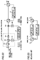
amplifier, as shown in FIG. 23 is of a simple parallel construction where an input
WDM signal light is demultiplexed by a demultiplexer into a C band and an L band,
and after being respectively amplified in a C band optical amplifying section and an L
band optical amplifying section, is multiplexed by a multiplexer and then output.
However, since the demultiplexer is provided on the input side of the
respective C band and the L band optical amplifying sections, there is a problem that
the noise figure deteriorates by the insertion loss portion. As a technique for coping
with this, there is known for example an optical amplifier disclosed for example in
"Optical Amplifiers and their Applications, Post deadline 2 of '97 published by
Lucent Technologies. A schematic construction of this is shown in the block
diagram of FIG. 24. With the construction of FIG. 24, a C/L band optical amplifying
section having an amplifying band in both the C band and the L band is arranged in
the pre-stage of the demultiplexer in the construction of FIG. 23. Hence at least a
gain equal to or greater than the insertion loss part of the demultiplexer is ensured
by the C/L band optical amplifying section, so that an improvement in the noise
figure is achieved.
However, with the above mentioned C/L band optical amplifier, there is the
drawback in that there are many cases where the noise figure for the C band optical
amplifying section and the noise figure for the L band optical amplifying section are
different, so that in general, the optical SN ratio for the optical signal of the L band
deteriorates compared to that for the optical signal of the C band. More specifically,
in the case where an optical fiber amplifier which uses rare earth element doped
fiber is employed in the optical amplifying sections of the respective bands, it is
known that the noise figure for the L band optical amplifying section deteriorates by
1dB.
Furthermore, with the optical amplifier of the construction as shown in FIG. 24,
since this has three or more optical fiber amplifier sections, the number of excitation
light sources also increases. As a result, the power consumption of the overall
optical amplifier increases. In particular, in the case where, as with optical amplifiers
used for example as undersea repeaters or the like, there are restrictions from the
view point of installation space, power consumption or other factors, it is difficult to
realize a construction such as shown in FIG. 24.
Furthermore, it is also important to control the balance of the optical power of
the C band and the L band. That is to say, in the case of a setting where the
number of optical signals (channel number) included in the respective bands is
different, or in the case where this setting is changed during operation, it is
necessary to appropriately control the respective operations of the optical amplifying
sections for the respective bands to ensure the required transmission characteristics.
SUMMARY OF THE INVENTION
The present invention focuses on the above points, with a first object of
providing an optical amplifier for performing amplification of optical signals of two
wavelength bands, wherein deterioration in the relative optical SN ratio for one
wavelength band is reduced. Moreover, a second object is to provide an optical
amplifier of a simple construction which can deal with restrictions on installation
space, power consumption and the like. Furthermore, a third object is to provide an
optical amplifier enabling the balance control of the optical power with respect to
respective wavelength bands is possible.
In order to achieve the abovementioned objects, a first aspect of an optical
amplifier according to the present invention for amplifying wavelength division
multiplexed signal light which contains respective optical signals of a first wavelength
band (for example 1550nm band etc.) and a second wavelength band (for example
1580nm band etc.), comprises an optical amplifying device for amplifying the
wavelength division multiplexed signal light using a rare earth element doped fiber to
which excitation light is supplied, wherein the excitation light used by the optical
amplifying device has a wavelength capable of producing Raman amplification with
respect to optical signals of the second wavelength band, and by supplying a part of
the excitation light used in the optical amplifying device to a Raman amplification
producing medium which forms at least a part of an external transmission path
arranged on a pre-stage side of the optical amplifying device, wavelength division
multiplexed signal light which contains optical signals of the second wavelength
band which have been Raman amplified by the Raman amplification producing
medium, are input to the optical amplifying device.
With such a construction, the optical signals of the second wavelength band
can be Raman amplified, by employing a part of the excitation light used in the
optical amplifying device. Hence the optical signals of the second wavelength band
which have been Raman amplified are amplified by the optical amplifying device. As
a result, the optical SN ratio for the second wavelength band is improved, and
optical signals with uniform characteristics in the respective wavelength bands can
be obtained.
As one specific construction for the above mentioned optical amplifier, there
may be provided a demultiplexing device for demultiplexing the wavelength division
multiplexed signal light into respective optical signals of a first wavelength band and
a second wavelength band, and a multiplexing device for multiplexing respective
optical signals of the first wavelength band and the second wavelength band which
have been demultiplexed by the demultiplexing device, and the optical amplifying
device may have a first amplifying section for amplifying optical signals of the first
wavelength band which have been demultiplexed by the demultiplexing device, and
a second amplifying section for amplifying optical signals of the second wavelength
band which have been demultiplexed by the demultiplexing device, the construction
being such that by supplying via the demultiplexing device a part of the excitation
light used in the first amplifying section to the Raman amplification producing
medium, optical signals of the second wavelength band which have been Raman
amplified by the Raman amplification producing medium, are input via the
demultiplexing device to the second optical amplifying section.
Furthermore, as another specific construction for the abovementioned optical
amplifier, there may be provided a demultiplexing device for demultiplexing the
wavelength division multiplexed signal light into respective optical signals of a first
wavelength band and a second wavelength band, and a multiplexing device for
multiplexing respective optical signals of the first wavelength band and the second
wavelength band which have been demultiplexed by the demultiplexing device, and
the optical amplifying device may have a pre-stage amplifying section for collectively
amplifying the wavelength division multiplexed signal light input to the demultiplexing
device, and a second optical amplifying section for amplifying only optical signals of
the second wavelength band which have been demultiplexed by the demultiplexing
device, the construction being such that by supplying a part of the excitation light
used in the pre-stage optical amplifying section to the Raman amplification
producing medium, wavelength division multiplexed signal light which contains
optical signals of the second wavelength band which have been Raman amplified by
the Raman amplification producing medium are input to the pre-stage optical
amplifying section.
Another aspect of an optical amplifier according to the present invention for
amplifying wavelength division multiplexed signal light which contains respective
optical signals of a first wavelength band (for example a 1550 nm band etc.) and a
second wavelength band (for example a 1580nm band etc.) may comprise a pre-stage
optical amplifying device for collectively amplifying respective optical signals of
the first wavelength band and the second wavelength band for the wavelength
division multiplexed signal light, a demultiplexing device for demultiplexing the
wavelength division multiplexed signal light which has been amplified by the pre-stage
amplifying device into optical signals of a first wavelength band and optical
signals of a second wavelength band, a post-stage optical amplifying device for
amplifying only optical signals of the second wavelength band which have been
demultiplexed by the demultiplexing device, and a multiplexing device for
multiplexing optical signals of the first wavelength band which have been
demultiplexed by the demultiplexing device, and optical signals of the second
wavelength band which have been amplified by the post-stage optical amplifying
device.
With such a construction, in the pre-stage optical amplifying device provided
at the input stage, the optical signals of the first wavelength band are amplified to a
sufficient level, while for the optical signals of the second wavelength band, the
insufficient gain portion is amplified by the post-stage optical amplifying device. As a
result, the construction can be simplified compared to the conventional optical
amplifier.
Furthermore, the abovementioned optical amplifier is preferably constructed
to comprise a first power monitor device for monitoring the optical signal power of
the first wavelength band which has been demultiplexed by the demultiplexing
device, a second power monitor device for monitoring the optical signal power of the
second wavelength band which has been amplified by the post-stage optical
amplifying device, and an optical power deviation control device for controlling the
operation of at least one of the pre-stage optical amplifying device and the post-stage
optical amplifying device in response to the respective monitor results of the
first and second power monitor devices, so that the optical power deviation for the
first and the second wavelength bands becomes constant.
With such a construction, balance control of the optical power of the first
wavelength band and the second wavelength band is performed. As a result, the
optical amplification for the respective wavelength bands can be more stably
performed. Moreover, it is possible to flexibly correspond to changes in the
channels being used.
By combining the two aspects of the optical amplifier according to the present
invention as described above, that is to say, by Raman amplifying the optical signals
of the second wavelength band using a part of the excitation light used in the optical
amplifying device, and omitting the first optical amplifying section for amplifying the
demultiplexed optical signals of the first wavelength band, the construction can be
simplified. Moreover, a construction is also possible where balance control for the
respective wavelength bands is performed.
Other objects, features and advantages of the present invention will become
apparent from the following description of embodiments given in conjunction with the
appended drawings.
BRIEF DESCRIPTION OF THE DRAWINGS
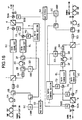
FIG. 1 is a block diagram showing a basic construction of an optical amplifier
according to a first embodiment of the present invention.
FIG. 2 is a diagram showing an example of a transmission path used in the
above mentioned first embodiment.
FIG. 3 is a diagram with wavelength characteristics related to gain per unit
length of a typical EDF shown for each population inversion rate.
FIG. 4 is a block diagram showing a basic construction of an optical amplifier
according to a second embodiment of the present invention.
FIG. 5 is a block diagram showing a construction of an optical amplifier
according to a third embodiment of the present invention.
FIG. 6 is a diagram showing another structural example related to the third
embodiment.
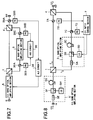
FIG. 7 is a block diagram showing a construction of an optical amplifier
according to a fourth embodiment of the present invention.
FIG. 8 is a block diagram showing a basic construction of an optical amplifier
according to a fifth embodiment of the present invention.
FIG. 9 is a block diagram showing a construction of an optical amplifier
according to a sixth embodiment of the present invention.
FIG. 10 is a diagram showing another structural example related to the sixth
embodiment.
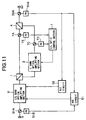
FIG. 11 is a block diagram showing a construction of an optical amplifier
according to a seventh embodiment of the present invention.
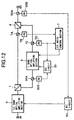
FIG. 12 is a diagram showing another structural example related to the
seventh embodiment.
FIG. 13 is a block diagram showing a basic construction of an optical
amplifier according to an eighth embodiment of the present invention.
FIG. 14 is a diagram showing a specific structural example (1) of the eighth
embodiment.
FIG. 15 is a diagram showing a specific structural example (2) of the eighth
embodiment.
FIG. 16 is a diagram showing a modified example related to the structural
example (2) of the eighth embodiment.
FIG. 17 is a diagram showing a specific structural example (3) of the eighth
embodiment.
FIG. 18 is a diagram showing a modified example related to the structural
example (3) of the eighth embodiment.
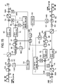
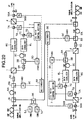
FIG. 19 is a diagram showing a specific structural example (4) of the eighth
embodiment.
FIG. 20 is a diagram showing a specific structural example (5) of the eighth
embodiment.
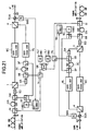
FIG. 21 is a diagram showing a specific structural example (6) of the eighth
embodiment.
FIG. 22 is a block diagram showing a schematic construction for where a
processing function for a supervisory control signal is provided in the respective
embodiments of the present invention.
FIG. 23 is a block diagram showing a construction of a conventional C/L band
optical amplifier.
FIG. 24 is a block diagram showing the construction of a conventional C/L
band optical amplifier for compensating insertion losses of a demultiplexing device.
EMBODIMENTS OF THE INVENTION
Hereunder is a description of embodiments of the present invention based on
the drawings.
FIG. 1 is a block diagram showing a basic construction of an optical amplifier
according to a first embodiment.
In FIG. 1, the present optical amplifier has a demultiplexer 1 serving as a
demultiplexing device for demultiplexing WDM signal light input from an external
transmission path L via a terminal IN, into a C band optical signal and an L band
optical signal, a C band optical amplifying section 2 serving as a first optical
amplifying section for amplifying the C band optical signals which have been
demultiplexed by the demultiplexer 1, an L band optical amplifying section 3 serving
as a second optical amplifying section for amplifying the L band optical signals which
have been demultiplexed by the demultiplexer 1, and a multiplexer 4 serving as a
multiplexing device for multiplexing optical signals which have been respectively
amplified by the C band optical amplifying section 2 and the L band optical
amplifying section 3, and outputting these to the outside via a terminal OUT.
Here, the C band corresponds to a first wavelength band. More specifically,
this represents a wavelength band (1550nm band) for example from 1525 to
1565nm. Furthermore, the L band corresponds to a second wavelength band. More
specifically, this represents a wavelength band (1580nm band) for example from
1565 to 1610nm. However, the first and second wavelength bands applicable to the
present invention, are not limited to the above mentioned range.
The C band optical amplifying section 2 includes for example an erbium
doped fiber (hereunder EDF) 2A, a WDM coupler 2B, an excitation light source (LD)
2C, and an optical isolator 2D.
The EDF 2A is a known rare earth doped fiber with erbium (Er) doped into an
optical fiber. The length etc. thereof is optimized so as to have an amplifying band at
least for the C band. The specific setting of this EDF 2A is described later. The
WDM coupler 2B is an optical coupler for supplying excitation light generated by the
excitation light source 2C, to the EDF 2A from a rear side. The excitation light source
2C is a typical light source which generates excitation light of a wavelength band (for
example 1480nm band etc.) which can excite the erbium inside the EDF 2A, and
which can produce Raman amplification inside the external transmission path L with
respect to L band optical signals. The optical isolator 2D is a typical optical
component which passes light only in a direction from the WDM coupler 2B towards
the multiplexer 4.
The L band optical amplifying section 3 comprises for example an optical
isolator 3A, a WDM coupler 3B, an EDF 3C, and an excitation light source (LD) 3D.
The optical isolator 3A only passes light in a direction from the demultiplexer
1 towards the WDM coupler 3B. The WDM coupler 3B is an optical coupler which
couples L band optical signals which have passed through the optical isolator 3A
with excitation light generated by the excitation light source 3D, and supplies this to
the EDF 3C. The EDF 3C is a known rare earth doped fiber with erbium doped into
an optical fiber. The length etc. thereof is optimized so as to have an amplifying
band only for the L band. The specific setting of this EDF 3C is also described later.
The excitation light source 3D is a typical light source which generates excitation
light of a wavelength band (for example the 980nm band or the 1480 band etc.)
which can excite the erbium inside the EDF 3C.
In the case where L band optical amplification is performed using the EDF, in
consideration of the influence of the generation of spontaneous emission (ASE) light,
in general this is made a forward excitation type construction. However, there is also
the case where excitation light is also supplied from the rear side of the EDF, that is
to say this is made a bidirection excitation type, to achieve an improvement in
excitation efficiency.
Furthermore, with the external transmission path L connected to the present
optical amplifier, an optical fiber designed with the non-linear effective cross section
reduced compared to a 1.3µm zero dispersion single mode fiber (SMF) generally
used as an optical transmission path, so that the production of Raman amplification
is facilitated, is used at least on the side connected to the terminal IN of the optical
amplifier.
More specifically, for example as shown in FIG. 2, it is suitable to employ a
hybrid transmission path which uses a positive dispersion fiber (for example a 1.3
µm zero dispersion SMF etc.) with a relatively large non-linear effective cross
section having a positive wavelength dispersion value and a positive dispersion
slope with respect to the signal light wavelength band, in a first half of a repeater
section (the output side of the optical amplifier), and a negative dispersion fiber RDF
with a relatively small non-linear effective cross section having a negative
wavelength dispersion value and a negative dispersion slope, in a last half of the
repeater section (the input side of the optical amplifier). By applying this hybrid
transmission path, the excitation light of 1480nm which has leaked out from the input
terminal of the optical amplifier is supplied to the RDF, so that effectively, Raman
amplification is produced with respect to the L band optical signal. Furthermore,
concurrent with this, the wavelength dispersion and dispersion slope produced by
the first half 1.3 µm zero dispersion SMF are compensated for by the last half RDF.
The technique for transmitting WDM signal light using such a hybrid transmission
path has been previously proposed by the present applicant (refer to Japanese
Patent Application No. 11-58499, and Japanese Patent Application No. 11-104158).
The transmission path L connected to the optical amplifier according to the
present invention is not limited to a hybrid transmission path such as described
above, and may be one where an optical fiber with a non-linear effective cross
section which is smaller than a 1.3µm zero dispersion SMF, is used over the entire
region of the repeater section. Moreover, as an optical fiber with a small non-linear
effective cross section, other than the above mentioned RDF, for example a
dispersion shifted fiber (DSF) or the like may be used.
Here is a description concerning the setting conditions for an EDF having an
amplifying band in the above mentioned C band or L band.
FIG. 3 is a diagram with wavelength characteristics related to gain per unit
length of a typical EDF shown for each population inversion rate (0.0 ∼ 1.0).
As shown in FIG. 3, for the C band (1550nm band), this has a positive gain
when the population inversion rate is approximately 0.55 or more. For the L band
(1580nm band), this has a positive gain when the population inversion rate is
approximately 0.4 or more, however, if the population inversion rate increases, the
wavelength dependency of the gain increases. For the L band, the population
inversion rate where a comparatively flat gain wavelength characteristic can be
obtained is around a range of 0.45 ∼ 0.55.
Consequently, with the C band optical amplification, the length and excitation
optical power of the EDF 2A is set so that the average population inversion rate in
the longitudinal direction of the EDF 2A is 0.55 or more. By so doing, the C band
optical signal can be amplified up to a required level. In the case of this setting,
although the L band optical signal can also be amplified, the gain thereof is smaller
than the gain of the C band with the characteristic that the gain deviation with
respective to wavelength is also large. On the other hand, with the L band optical
amplification, the length and excitation optical power of the EDF 3C is set so that the
average population inversion rate in the longitudinal direction of the EDF 3C is in the
range of 0.45 ∼ 0.55. By so doing, only the L band optical signal can be amplified at
a flat gain wavelength characteristic. The L band optical amplification with such a
low population inversion rate can be realized, with a method such as where the
typical EDF used in the C band optical amplification is lengthened and the
population inversion rate reduced.
Here is a brief description concerning the above mentioned Raman
amplification.
Raman amplification is a phenomenon where, by supplying a required
excitation light to a Raman amplification producing medium, an optical signal
propagated inside the Raman amplification producing medium is amplified. The
wavelength band where Raman amplification is produced is known to change in
accordance with the wavelength band of the Raman excitation light. More
specifically, with a wavelength band used for optical communication, it can be
considered that Raman amplification is produced in a wavelength band shifted from
a Raman excitation light wavelength by approximately 100nm to the long
wavelength side. Furthermore, Raman amplification has the characteristic of being
easily produced in an optical fiber where the non-linear effective cross section is
small. Consequently, with the construction shown in FIG. 1, in the C band optical
amplifying section 2, Raman amplification is produced with respect to optical signals
of the L band (1580nm band) inside the small non-linear effective cross section RDF
of the transmission path L to which the excitation light of the wavelength 1480nm
band output from the excitation light source 2C is supplied.
Next is a description of the operation of the optical amplifier of the first
embodiment.
With the present optical amplifier, due to the excitation light of the 1480nm
band leaked out to the transmission path L from the C band optical amplifying
section 2 via, the demultiplexer 1 and the terminal IN, Raman amplification is
produced in the transmission path L with respect to the L band optical signal, and
the WDM signal light which contains the L band optical signals which have been
Raman amplified, is input to the demultiplexer 1 via the terminal IN.
In the demultiplexer 1, the input WDM signal light is demultiplexed for each of
the respective bands, and the C band optical signal is sent to the C band amplifying
section 2, and the L band optical signal is sent to the L band optical amplifying
section 3. In the C band optical amplifying section 2, the optical signal from the
demultiplexer 1 is sent to the EDF 2A. The excitation light from the excitation light
source 2C is supplied to the EDF 2A via the WDM coupler 2B to give the excited
condition of the EDF 2A. Then, the C band optical signal is propagated inside the
EDF 2A and amplified to a required level by the induced emission. The amplified C
band optical signals are then sent to the multiplexer 4 via the WDM coupler 2B and
the optical isolator 2D.
In the L band optical amplifying section 3, the Raman amplified L band optical
signal which has been sent from the demultiplexer 1, is sent to the EDF 3C via the
optical isolator 3A and the WDM coupler 3B. The excitation light of the wavelength
1480nm band from the excitation light source 3D is supplied to the EDF 3C via the
WDM coupler 3B to give the excited condition of the EDF 3C. Then, the L band
optical signal is propagated inside the EDF 3C and amplified to a required level by
the induced emission.
Optical signals of each band which have been respectively amplified by the C
band optical amplifying section 2 and the L band optical amplifying section 3 are
sent to the multiplexer 4 to be multiplexed, and then output to the outside of the
present amplifier via the terminal OUT.
With the first embodiment as described above, the construction is such that
the excitation light of the 1480nm band supplied to the EDF 2A in the C band optical
amplifying section 2 is leaked out to the external transmission path L via the
demultiplexer 1 and the terminal IN, and by using a part of the excitation light to the
EDF 2A to produce Raman amplification in the transmission path L, the optical
signal level of the L band which is contained in the WDM signal light input to the
present optical amplifier, increases. Therefore, the optical SN ratio of the L band
optical signal output from the L band optical amplifying section 3 can be improved.
As a result, the optical SN ratio where heretofore the L band is deteriorated
compared to the C band, can be given approximately the same characteristics by
using Raman amplification.
Next is a description of a second embodiment of the present invention.
FIG. 4 is a diagram showing a basic construction of an optical amplifier
according to the second embodiment. Parts of the same construction as for the first
embodiment are denoted by the same reference numerals. The same applies for
the subsequent figures.
In FIG. 4, the optical amplifier has a C/L band optical amplifying section 5 as
a pre-stage amplification section for amplifying WDM signal light input from an
external transmission path L via a terminal IN, a demultiplexer 1 for demultiplexing
optical signals which have been amplified by the C/L band optical amplifying section
5 into a C band optical signal and an L band optical signal, an L band optical
amplifying section 3 for amplifying L band optical signals which have been
demultiplexed by the demultiplexer 1, and a multiplexer 4 for multiplexing the C band
optical signals which have been demultiplexed by the demultiplexer 1, and the L
band optical signals which have been amplified by the L band optical amplifying
section 3, and outputting these to an external transmission path L via a terminal
OUT.
The C/L band optical amplifying section 5 comprises for example an EDF 5A,
a WDM coupler 5B, an excitation light source (LD) 5C, and an optical isolator 5D.
With the EDF 5A, one end is connected to the terminal IN, and the other end
is connected to the WDM coupler 5B, and excitation light generated by the excitation
light source 5C is supplied from a rear side via the WDM coupler 5B. With this EDF
5A, the length thereof is optimized so that this has an amplification band for both the
C band and the L band. More specifically, as with the case for the optical
amplification of the C band described above using FIG. 3, the length etc. is set so
that the average population inversion rate in the longitudinal direction of the EDF 5A
is 0.55 or more. As a result, the respective optical signals of the C band and the L
band are amplified. However, for the optical amplification of the L band, the
characteristics are such that the gain thereof is very much smaller than the gain for
the C band, and the gain wavelength characteristics also have a comparatively large
slope. The excitation light source 5C is a typical light source which can excite the
erbium inside the EDF 5A, and which generates excitation light of a wavelength
band (for example the 1480nm band) which can activate Raman amplification inside
the external transmission path L with respect to the L band optical signal. The
optical isolator 5D passes only light in a direction from the WDM coupler 5B towards
the demultiplexer 1.
The demultiplexer 1, the L band optical amplifying section 3 and the
multiplexer 4 are the same as those used in the first embodiment, and hence
description is omitted. Furthermore, for the external transmission path L connected
to the present optical amplifier, as with the case of the first embodiment, an optical
fiber where the non-linear effective cross section is small compared to the typical
1.3µm zero dispersion SMF so that Raman amplification can be easily produced, is
at least used on the side connected to the terminal IN of the optical amplifier.
Preferably a hybrid transmission line as shown in FIG. 2 is used with two types of
optical fiber connected together.
Next is a description of the operation of the optical amplifier of the second
embodiment.
With the present optical amplifier, due to the excitation light of the 1480nm
band leaked out to the transmission path L from the C/L band optical amplifying
section 5 via the terminal IN, Raman amplification is produced in the transmission
path L with respect to the L band optical signals, and the WDM signal light which
contains the L band optical signals which have been Raman amplified, is input to the
C/L band optical amplifying section 5 via the terminal IN.
With the WDM signal light input to the C/L band optical amplifying section 5,
the respective optical signals of the C band and the L band are collectively amplified.
By means of the amplifying affect of the C/L band optical amplifying section 5,
insertion losses in at least the post-stage demultiplexer 1 are compensated for.
The WDM signal light output from the C/L band optical amplifying section 5 is
demultiplexed for each of the respective bands by the demultiplexer 1, and the L
band optical signals are sent to the L band optical amplifying section 3. In the L
band optical amplifying section 3, as with the case of the first embodiment, the L
band optical signals are amplified to a required level by induced emission. Then, the
C band optical signals demultiplexed by the demultiplexer 1, and the L band optical
signals amplified by the L band optical amplifying section 3 are sent to the
multiplexer 4 and coupled, and then output to the transmission path L via the
terminal OUT.
As described above, with the second embodiment, the construction is such
that there is provided the C/L band optical amplifying section 5 between the terminal
IN and the demultiplexer 1, and in the C/L band optical amplifying section 5, the
excitation light of the 1480nm band supplied to the EDF 5A leaks out to the external
transmission path L via the terminal IN. Furthermore, since the input level of the L
band optical signal input to the present optical amplifier increases by producing
Raman amplification in the transmission path L with respect to the L band optical
signal, the optical SN ratio of the L band optical signal for the overall optical amplifier
can be improved. As a result, the optical SN ratio where heretofore the L band is
deteriorated compared to the C band, can be given approximately the same
characteristics by using Raman amplification. Of course, as with the conventional
case, since the insertion losses of the demultiplexer 1 are also compensated for by
the C/L band optical amplifying section 5, there is also the effect of suppressing
deterioration of the noise figure due to insertion of the demultiplexer 1.
Next is a description of a third embodiment of the present invention.
With the third embodiment, the case is considered where for example in the
second embodiment described above, compensation for the wavelength dispersion
and dispersion slope, or compensation for the gain wavelength characteristics can
be executed inside the optical amplifier.
FIG. 5 shows a structural example of an optical amplifier according to the
third embodiment.
In FIG. 5, the construction of the present optical amplifier is such that
compensation optical devices 6C and 6L are respectively provided on the light
transmission paths corresponding to the respective bands, between the
demultiplexer 1 and the multiplexer 4. Here, the compensation optical device 6C
corresponding to the C band is inserted between the demultiplexer 1 and the
multiplexer 4, while the compensating optical device 6L corresponding to the L band
is inserted between the L band optical amplifying section 3 and the multiplexer 4.
The insertion position of the compensating optical device 6L, while not shown in the
figure, may be between the demultiplexer 1 and the L band optical amplifying section
3.
For the respective compensating optical devices 6C and 6L, for example
these may be typical optical passive parts such as a dispersion compensating fiber
(DCF) or a fiber grating used for compensating for wavelength dispersion and
dispersion slope which are produced and accumulates in the transmission path L
connected to the present optical amplifier. Alternatively, these may be known gain
equalizers having a loss wavelength characteristic corresponding to the gain
wavelength characteristics of the C/L band optical amplifying section 5 or the L band
optical amplifying section 3. In the case where dispersion compensation and
compensation for gain wavelength characteristics are carried out at the same time, a
DCF and a gain equalizer may be cascade connected for each of the respective
bands.
By having the above described construction, then in addition to the
operational effect for the case of the second embodiment, wavelength dispersion
and dispersion slope or gain deviation between respective wavelengths are
compensated for inside the optical amplifier. Hence the transmission characteristics
of the WDM signal light can be improved.
With the above described third embodiment, the construction is such that
there is provided a compensation optical device for each of the respective bands.
However for example as shown in FIG. 6, a compensation optical device 6CL which
can perform compensation for the C band and the L band collectively, may be also
provided between the multiplexer 4 and the terminal OUT.
Next is a description of a fourth embodiment of the present invention.
With the fourth embodiment, the case is considered where for example in the
second embodiment described above, automatic level control (ALC) for controlling
the output from the optical amplifier to be constant, and automatic gain control
(AGC) for controlling the gain in the optical amplifier to be constant, are executed.
FIG. 7 shows a structural example of an optical amplifier according to the
fourth embodiment.
In FIG. 7, the present optical amplifier is constructed such that there is
provided an AGC circuit 30 for the L band optical amplifying section 3, and there is
provided an ALC circuit 50 for the C/L band optical amplifying section 5.
The AGC circuit 30 uses a signal for where a part of the L band optical signal
for input to the L band optical amplifying section 3 is branched by an optical coupler
30A, and photoelectrically converted by a photodetector 30B, and a signal for where
a part of the optical signal output from the L band optical amplifying section 3 is
branched by an optical coupler 30C and photoelectrically converted by a
photodetector 30D, to compute a gain in the L band optical amplifying section 3, and
outputs to the L band optical amplifying section 3, a control signal for controlling the
amplification operation so that this gain becomes constant. In the L band optical
amplifying section 3 which receives the control signal from the AGC circuit 30, for
example the injection current or the like of the excitation light source 3D is adjusted
according to the control signal.
The ALC circuit 50 compares the signal for where a part of the WDM signal
light output from the multiplexer 4 is branched by an optical coupler 50A and
photoelectrically converted by a photodetector 50B, with a previously set reference
signal, and outputs to the C/L band optical amplifying section 5, a control signal for
controlling the amplification operation so that the level of the WDM signal light output
from the present optical amplifier becomes constant. In the C/L band optical
amplifying section 5 which receives the control signal from the ALC circuit 50, for
example the injection current or the like of the excitation light source 5C is adjusted
according to the control signal.
As described above, with the fourth embodiment, in addition to the effect for
the case of the second embodiment, by subjecting the L band optical amplifying
section 3 to AGC operation, then even in the case where the input light level of the L
band changes, fluctuations in the gain wavelength characteristics are suppressed.
Hence stable optical amplification can be performed. Furthermore, by monitoring
the output optical level and subjecting the C/L band optical amplifying section 5 to
ALC operation, then even in the case where the input light level to the present
optical amplifier changes, a constant level WDM signal light can be output. Hence
stabilized amplification repeater transmission for the WDM signal light becomes
possible.
With the above fourth embodiment, the case is shown for where AGC and
ALC are executed concurrently, however control with only one of AGC and ALC can
be applied. Furthermore, for the first and third embodiments also, AGC and ALC
may be similarly executed. In the case where ALC is applied to the first embodiment,
the respective amplification operation for the C band optical amplifying section 2 and
the L band optical amplifying section 3 may be adjusted in accordance with the
control signal of the ALC circuit.
Next is a description of a fifth embodiment of the present invention.
With the above described first through fourth embodiments, a part of the
excitation light of the 1480nm band supplied to the EDF is used to produce Raman
amplification with respect to the L band optical signal, to thereby improve the optical
SN ratio for the L band. With the fifth embodiment, a technique is described for
adding an improvement from the viewpoint of simplification of the construction in a
conventional optical amplifier which collectively amplifies the C band and the L band
optical signals.
FIG. 8 is a block diagram showing a basic construction of an optical amplifier
according to the fifth embodiment.
In FIG. 8, the present optical amplifier is constructed with the C band optical
amplifier in the conventional construction shown in FIG. 24 omitted, and the function
of this amplifier is provided in a pre-stage C/L band optical amplifying section 5' and
a C/L ratio control section 7 serving as an optical power deviation control device is
provided for controlling a balance between the C band optical signal power and the L
band optical signal power. A demultiplexer 1 for demultiplexing the WDM signal light
output from the C/L band optical amplifying section 5' into a C band and an L band,
an L band optical amplifying section 3 corresponding to a post-stage optical
amplifying device, and a multiplexer 4 for multiplexing the demultiplexed C band
optical signals and the L band optical signals which have been amplified by the L
band optical amplifying section 3, are the same as the components used in the
aforementioned first embodiment.
The C/L band optical amplifying section 5' corresponding to the pre-stage
optical amplifying device, comprises for example an optical isolator 5E, a WDM
coupler 5F, an EDF 5G, and an excitation light source (LD) 5H.
The optical isolator 5E is a device for passing only light in a direction from the
terminal IN towards the WDM coupler 5F. The WDM coupler 5F couples the WDM
signal light which has passed through the optical isolator 5E with excitation light from
the excitation light source 5H, and supplies this to the EDF 5G from the front side.
For the EDF 5G, similarly to the EDF 5A used in the beforementioned second
embodiment (FIG. 4), the length etc. is optimized so as to have an amplifying band
for both the C band and the L band. The excitation light source 5H is a typical light
source for generating excitation light of a wavelength band (for example a 980nm
band or a 1480nm band etc.) which can excite the erbium inside the EDF 5G. Here
the construction is for a forward excitation type, however a construction for a
backward excitation type or a bidirection excitation type is also possible.
The C/L ratio control section 7 outputs a control signal for controlling the
amplification operation of the L band optical amplifying section 3 based on a signal
for where a part of the optical signal of the C band output from the demultiplexer 1 is
branched by an optical coupler 7A and photoelectrically converted by a
photodetector (PD) 7B, and a signal for where a part of the optical signal output from
the L band optical amplifying section 3 is branched by an optical coupler 7C and
photoelectrically converted by a photodetector 7D. Here the optical coupler 7A and
the photodetector 7B correspond to a first power monitor device, and the optical
coupler 7C and the photodetector 7D correspond to a second power monitor device.
With the optical amplifier of the above described construction, the WDM
signal light which has been input via the terminal IN is sent to the C/L band optical
amplifying section 5', and the respective optical signals of the C band and the L band
are collectively amplified. By means of the amplifying affect of the C/L band optical
amplifying section 5', the C band optical signal is amplified to a required output level
or above. Furthermore, for the L band optical signal, the insertion losses in at least
the post-stage demultiplexer 1 are compensated for.
The WDM signal light output from the C/L band optical amplifying section 5' is
demultiplexed for each of the respective bands by the demultiplexer 1, and the L
band optical signals are sent to the L band optical amplifying section 3. In the L
band optical amplifying section 3, the L band optical signals are amplified to a
required level by induced emission.
Then, the C band optical signals which have been demultiplexed by the
demultiplexer 1, and the L band optical signals which have been output from the L
band optical amplifying section 3 are passed through the optical couplers 7A and 7C,
respectively, and then multiplexed by the multiplexer 4, and output from the terminal
OUT. Together with this, a part of these optical signals is branched by the optical
couplers 7A and 7C and then sent to the C/L ratio control section 7 via the
photodetectors 7B and 7D. In the C/L ratio control section 7, a control signal is
output for controlling the amplification operation of the L band optical amplifying
section 3 based on signals from the respective photodetectors 7B and 7D, so that
the C band optical signal power and the L band optical signal power become a
previously set ratio. More specifically, for example in the case of a situation where a
32 channel optical signal is used for the C band, and a 16 channel optical signal is
used for the L band (to make the optical power of the respective channels the same),
a control signal is generated for controlling the amplification operation of the L band
optical amplifying section 3 so that the ratio of the C band optical signal power and
the L band optical signal power becomes constant at 2: 1. In the L band optical
amplifying section 3 which has received the control signal from the C/L ratio control
section 7, for example the injection current or the like of the excitation light source
3D is adjusted according to the control signal.
In the above manner, the construction is such that, in the fifth embodiment,
for the C/L band optical amplifying section 5' provided in the input stage, the
construction is such that the C band optical signal is amplified to a sufficient level,
while the L band optical signal, only for the insufficient gain portion, is amplified by
the post-stage L band optical amplifying section 3. As a result, simplification of the
construction compared to for the conventional optical amplifier can be achieved.
This is particularly useful when the installation space or power consumption is limited,
such as in the case for example where the optical amplifier is employed as an
undersea repeater, since the number of parts for the excitation light source can be
reduced. However, the optical amplifier of the present invention is not limited to the
above use. For example by enabling control of the balance of the optical power of
the C band and the L band, the optical amplification of the respective bands can be
carried out more stably, and also it is possible to flexibly correspond for example to
changes etc. in the channels used for the respective bands.
With the fifth embodiment, the construction is such that balance control is
performed for the optical power of the C band and the L band. However with a
system construction where such control is not necessary, the C/L ratio control
section 7, the optical couplers 7A and 7C and the photodetectors 7B and 7D can be
omitted.
Next is a description of a sixth embodiment of the present invention.
With the sixth embodiment, the case is considered where in the fifth
embodiment, compensation for the wavelength dispersion and dispersion slope, or
compensation for the gain wavelength characteristics can be executed inside the
optical amplifier.
FIG. 9 shows a structural example of an optical amplifier according to the
sixth embodiment.
In FIG. 9, the construction of the present optical amplifier, as with the case of
the third embodiment described above, is such that compensation optical devices
6C and 6L are respectively provided on the light transmission paths corresponding
to the respective bands between the demultiplexer 1 and the multiplexer 4. Here the
compensation optical device 6C corresponding to the C band is inserted between
the demultiplexer 1 and the optical coupler 7A, while the compensating optical
device 6L corresponding to the L band is inserted between the L band optical
amplifying section 3 and the optical coupler 7C. For the respective compensating
optical devices 6C and 6L, for example, these may be typical optically passive parts
such as a dispersion compensating fiber (DCF) or a fiber grating, or these may be
known gain equalizers. The insertion position for the respective compensation
optical devices 6C and 6L is not limited to the abovementioned positions, and these
may be optionally positioned on the respective light transmission paths between the
demultiplexer 1 and the multiplexer 4.
In this manner, with the sixth embodiment, in addition to the operational effect
for the case of the fifth embodiment, wavelength dispersion and dispersion slope or
gain deviation between respective wavelengths is compensated inside the optical
amplifier. Hence the transmission characteristics of the WDM signal light can be
improved.
With the above described sixth embodiment, the construction is such that
there is provided a compensation optical device for each of the respective bands.
However for example as shown in FIG. 10, a compensation optical device 6CL
which can perform compensation for the C band and the L band collectively, may be
also provided between the multiplexer 4 and the terminal OUT.
Next is a description of the seventh embodiment of the present invention.
With the seventh embodiment, the case is considered where in the fifth
embodiment described above, automatic level control (ALC) for controlling the
output from the optical amplifier to be constant, and automatic gain control (AGC) for
controlling the gain in the optical amplifier to be constant are executed.
FIG. 11 shows a structural example of an optical amplifier according to the
seventh embodiment.
In FIG. 11, the present optical amplifier is constructed such that there is
provided an ALC circuit 50 and an AGC circuit 51 for the C/L band optical amplifying
section 5'. The ALC circuit 50, as with the case of the fourth embodiment, compares
the signal for where a part of the WDM signal light output from the multiplexer 4 is
branched by an optical coupler 50A and photoelectrically converted by a
photodetector 50B, with a previously set reference signal, and outputs to the C/L
band optical amplifying section 5', a control signal for controlling the amplification
operation so that the level of the WDM signal light output from the optical amplifier
becomes constant.
The AGC circuit 51 uses a signal for where a part of the WDM signal light for
input to the C/L band optical amplifying section 5' is branched by an optical coupler
51A, and photoelectrically converted by a photodetector 51B, and a monitor signal
for the output light used in the ALC (the signal via the optical coupler 50A and the
photodetector 50B), to compute a gain in the overall optical amplifier, and outputs to
the C/L band optical amplifying section 5', a control signal for controlling the
amplification operation so that this gain becomes constant.
In the C/L band optical amplifying section 5' which receives the respective
control signals from the ALC circuit 50 and the AGC circuit 51, for example the drive
condition or the like of the excitation light source 5C is adjusted according to the
respective control signals.
In the above manner, with the seventh embodiment, in addition to the
operational effect for the case of the fifth embodiment, by operating the C/L band
optical amplifying section 5' under the control of ALC and AGC, then even in the
case where the input optical level changes, a constant level WDM signal light can be
output. Moreover, changes in the gain wavelength characteristics can be
suppressed, and amplification of the WDM signal light can be stably performed.
With the seventh embodiment, the case is shown for where AGC and ALC
are executed concurrently, however control with only one of AGC and ALC can be
applied. Furthermore, the C/L band optical amplifying section 5' is constructed for
AGC operation. However the L band optical amplifying section 3 may be for AGC
operation. More specifically, as shown in FIG. 12, an AGC circuit 30 may be
provided, and a signal for where a part of the light signal for input to the L band
optical amplifying section 3 is branched by an optical coupler 30A, and
photoelectrically converted by a photodetector 30B, and a monitor signal of the L
band used in the C/L ratio control (the signal via the optical coupler 7C and the
photodetector 7D), are used to compute a gain in the L band optical amplifying
section 3, and a control signal for controlling the amplification operation so that this
gain becomes constant then is sent from the AGC circuit 30 to the L band optical
amplifying section 3. Furthermore, the above mentioned construction of FIG. 11 or
FIG. 12 may also be applied to the sixth embodiment.
Next is a description of an eighth embodiment of the present invention.
With the eighth embodiment, the description is given for the case where the
first through fourth embodiments which use Raman amplification, and the fifth
through seventh embodiments with simplified construction, and for which balance
control for each band is possible, are combined together.
FIG. 13 is a block diagram showing a basic construction of an optical
amplifier according to the eighth embodiment.
As shown in FIG. 13, with the present optical amplifier, the C band optical
amplifying section 2 in the construction of the second embodiment shown in FIG. 4
is omitted, and the function of this amplifying section is provided in a pre-stage C/L
band amplifier section 5. Moreover, as with the case of the fifth embodiment, there
is provided the C/L ratio control section 7, the optical couplers 7A and 7C, and the
photodetectors 7B and 7D, and balance control is performed for the optical power of
the C band and the L band.
The construction of the C/L band optical amplifying section 5, as with the
case of the second embodiment, is such that a part of the excitation light of the
1480nm band supplied from the rear side to the EDF 5A, is leaked out to the
transmission path L via the terminal IN. For the transmission path L connected to
the optical amplifier is an optical fiber where the non-linear effective cross section is
small compared to the 1.3µm zero dispersion SMF so that Raman amplification can
be easily produced, and is at least used on the side connected to the terminal IN of
the optical amplifier.
With the optical amplifier of the abovementioned construction, due to the
excitation light of the 1480nm band leaked out to the transmission path L from the
C/L band optical amplifying section 5, Raman amplification is produced in the
transmission path L with respect to the L band optical signals, and the WDM signal
light which contains the L band optical signals which have been Raman amplified, is
input to the C/L band optical amplifying section 5 via the terminal IN, and the
respective optical signals of the C band and the L band are collectively amplified by
the induced emission.
The WDM signal light output from the C/L band optical amplifying section 5 is
demultiplexed for each of the respective bands by the demultiplexer 1, and the L
band optical signals are sent to the L band optical amplifying section 3 and amplified
to a required level by induced emission. Then, the C band optical signals
demultiplexed by the demultiplexer 1, and the L band optical signals output from the
L band optical amplifying section 3, are multiplexed by the multiplexer 4 and output
to the transmission path L via the terminal OUT. Moreover, a part of these optical
signals are sent to the C/L ratio control section 7 via the optical couplers 7A and 7C,
and the photodetectors 7B and 7D respectively, and balance control of the C band
and the L band is executed.
In this way, with the eighth embodiment, by having the construction where the
C band optical signal is amplified to a sufficient level in the C/L band optical
amplifying section 5, using the C/L band optical amplifying section 5 of a
construction where the excitation light of the 1480nm band leaks out to the
transmission path L, while the L band optical signal, only for the insufficient gain
portion, is amplified by the post-stage L band optical amplifying section 3, an optical
amplifier where an improvement is achieved in the optical SN ratio for the L band
optical signal by the Raman amplification in the transmission path L, can be realized
with a simple construction. As a result, an optical amplifier of reduced power
consumption which can collectively amplify wide band WDM signal light, with
excellent characteristics can be provided. Furthermore, by enabling balance control
of the C band and the L band, optical amplification for the respective bands can be
more stably performed, and can also flexibly correspond to changes etc in the
channels being used.
As with the case of the sixth embodiment, while not shown in the figure,
compensation optical devices are respectively provided corresponding to each band,
and compensation for the wavelength dispersion and dispersion slope, or
compensation for the gain wavelength characteristics can be executed inside the
optical amplifier.
Furthermore, as with the case of the seventh embodiment, at the time of
executing ALC and AGC, the construction as shown in FIG. 12 is suitable. As
shown in FIG. 11, with the construction where the C/L band optical amplifying
section is AGC operated, in order to monitor the input level it is necessary to insert
an optical coupler at a pre-stage of the C/L band amplifier section. However, since
excitation light from the C/L band optical amplifying section towards the transmission
path is attenuated by the optical coupler, there is a situation where application of the
construction shown in FIG. 11 to the eighth embodiment is difficult.
Next, for the abovementioned eighth embodiment, specific structural
examples are further enumerated hereunder corresponding to an up line and a down
line. Components of the down line corresponding to the up line are denoted by the
same reference numerals.
With a structural example (1) of the optical amplifier shown in FIG. 14, the
construction is such that for the basic construction shown in FIG. 13, there is
provided compensation optical devices (here for example gain equalizers) 6C and
6L corresponding to the respective bands, and the C/L band optical amplifying
section 5 is ALC operated. These constructions are provided respectively to the up
line and the down line. For the excitation wavelength of the L band optical
amplifying section 3, either the 980nm band or the 1480nm band may be selected.
In the case of the 980nm band, a low noise and low power consumption are possible,
while with the 1480nm band, a high output is possible.
With the abovementioned construction, C band and L band optical
amplification can be executed with as little as four excitation light sources for the up
line and down line, and the improvement effect in optical SN ratio of the L band due
to Raman amplification is also obtained. Furthermore, a constant level WDM signal
light can be output by ALC operation, and balance control of the optical power of the
C band and the L band is also possible. Moreover, this construction also has the
advantage in that the up line and down line can be controlled independently and
individually.
A structural example (2) of the optical amplifier shown in FIG. 15 achieves an
improvement in the excitation efficiency by having the L band optical amplifying
section as a bidirection excitation type construction. Here, for the respective up and
down lines, excitation light of the 980 nm band output from the excitation light source
3D is supplied from the front side to the EDF 3C via the optical coupler 3B.
Moreover, excitation light of the 1480 nm band output from an excitation light source
3H which is used in common for the up and down lines, is supplied from the rear
side to the EDF 3C via optical couplers 3G and 3F.
With the above described construction, by adding one excitation light source
of the 1480nm band to the structural example (1) shown in FIG. 14, then for the
respective up and down lines, L band optical amplification with excellent excitation
efficiency can be realized. Other operational effects are the same as for the case of
structural example (1).
Here, with the above described example, the construction is such that the
rear excitation light source of the L band optical amplifying section is used in
common for the up and down lines. However instead of this, for example as shown
in FIG. 16, an excitation light source 5C of the 1480nm band between the C/L band
optical amplifying section and the L band optical amplifying section, may also be
used in common with each of the up line and the down line.
A structural example (3) of the optical amplifier shown in FIG. 17, achieves an
improvement in the noise figure by having a construction of a bidirection excitation
type where front excitation light is supplied to the C/L band optical amplifying section.
Here, for the respective up and down lines, excitation light of the 980nm band output
from the excitation light source 3D is branched in two by an optical coupler 3H, and
the branched respective excitation lights are supplied from the front side to the EDFs
5A and 3C via optical couplers 5I and 3B. Further, the branching ratio for the optical
coupler 3H is set so that the excitation optical power supplied to the L band optical
amplifying section is greater than the excitation optical power supplied to the C/L
band optical amplifying section.
With the abovementioned construction, a part of the excitation light used for L
band optical amplification, is used as front excitation light for the C/L band optical
amplifying section. In this way, the noise figure for the C/L band optical amplifying
section can be improved without increasing the number of excitation light sources.
Other operational effects are the same as for the case of structural example (1).
In the case where an excitation light of the 1480nm band is used for L band
optical amplification, then for example as shown in FIG. 18, an excitation light source
5J of the 980nm band may be separately provided for front excitation of the C/L
band optical amplifying section.
A structural example (4) of the optical amplifier shown in FIG. 19 is one where
the structural example (2) shown in FIG. 15 and the structural example (3) shown in
FIG. 17 are combined together. By having this construction, an improvement in the
excitation efficiency of the L band optical amplifying section, and an improvement in
noise figure of the C/L band optical amplifying section can be achieved.
A structural example (5) of the optical amplifier shown in FIG. 20 is one where
for example with the structural example shown in FIG. 18, the front excitation light
source of the C/L band optical amplifying section is made a redundant construction.
Here, the front excitation light used in the respective up and down C/L band optical
amplifying sections, at the time of normal operation, is supplied from the normal
excitation light source 5J of the 980nm band via an optical coupler 5K, and in the
case where an abnormality occurs in the normal excitation light source 5J, there is
made a switching to a standby excitation light source 5J' of the 980nm band.
With the above construction, since one of the excitation light sources of the
C/L band optical amplifying section is made redundant in the up and down lines, a
fail-safe optical amplifier construction can be realized. Other operational effects are
the same as for the case of structural example (3).
A structural example (6) of the optical amplifier shown in FIG. 21 is one where
the structural example shown in FIG. 16 and the structural example shown in FIG.
20 are combined together, and the number of excitation light sources is thus
reduced. More specifically, for each of the up and down lines, the rear excitation
light source of the C/L band optical amplifying section, and the rear excitation light
source of the L band optical amplifying section are used in common, and the
excitation lights of the 980nm band output from the excitation light sources 5J and
5J' of the redundant construction used in common in the up and down lines, are
respectively supplied from the front side to the C/L band optical amplifying section
and the L band optical amplifying section, via optical couplers 5K and 5L.
With the above described construction, with only four excitation light sources
for the up and down lines, the C/L band optical amplifying section and the L band
optical amplifying section can be made bidirection excitation type, respectively.
Moreover, since the respective front excitation light sources are made redundant in
the up and down lines, a fail-safe optical amplifier construction can be realized.
In FIG. 21, the construction for the C/L ratio control section 7 for controlling
the balance of the optical power of the C band and the L band has been omitted.
However depending on requirements for the balance control, the C/L ratio control
section 7 may appropriately be provided.
Moreover, the above described respective structural examples (1) through (6)
are examples of specific structures for the eighth embodiment. However the present
invention is not limited to these structural examples. Moreover, with the respective
structural examples, AGC is not executed. However the construction may be such
that the respective L band optical amplifying sections for the up and down lines are
AGC operated. In addition, specific structural examples for embodiments other than
the eighth embodiment can be easily realized based on the respective structural
examples (1) through (6) etc, and hence description here is omitted.
Here, is a description of a construction for the case where the respective
optical amplifiers shown in the first through eighth embodiments are applied to a
WDM optical repeater transmission system where a supervisory control signal is
transmitted from an optical transmission terminal or the like to a repeater station,
FIG. 22 is a block diagram showing a schematic construction of an optical
amplifier provided with a processing function for a supervisory control signal.
As shown in FIG. 22, a processing function for a supervisory control signal is
realized for example by an optical coupler 8A provided between the C/L band optical
amplifying section 5 and the demultiplexer 1, a photodetector (PD) 8B for converting
signal lights branched by the optical coupler 8A into electrical signals, and a
supervisory control processing section 8 for detecting a monitoring signal (SV
command signal) sent from an optical transmission terminal side to a repeater
station (optical amplifier), based on a signal from the photodetector 8B, and sending
a modulation signal corresponding to a response signal (SV response signal) sent
from the repeater station to an optical receiving terminal side, to the excitation light
source 5C. Here the monitoring signal and the response signal are transmitted by
superimposingly modulating the WDM signal light with a low frequency.
The supervisory control processing section 8 discriminates information
related to the transmission condition of the WDM signal light, based on the detected
monitoring signal (for example the number of the channel being used, and the
number of the channels etc.) and transmits this to the respective sections inside the
optical amplifier. Furthermore, this produces a modulation signal corresponding to
the response signal showing discriminated information or the operating
circumstances of the self-station. By modulating the excitation light source 5C
according to this modulation signal, the response signal is superimposed on the
WDM signal light.
In this way, by providing the optical amplifier with a function for processing
supervisory control signals, optical amplification corresponding to the transmission
circumstances of the WDM signal light can be performed.