EP1091442A2 - Circuit for dealing with higher harmonics and circuit for amplifying power efficiency - Google Patents
Circuit for dealing with higher harmonics and circuit for amplifying power efficiency Download PDFInfo
- Publication number
- EP1091442A2 EP1091442A2 EP00121758A EP00121758A EP1091442A2 EP 1091442 A2 EP1091442 A2 EP 1091442A2 EP 00121758 A EP00121758 A EP 00121758A EP 00121758 A EP00121758 A EP 00121758A EP 1091442 A2 EP1091442 A2 EP 1091442A2
- Authority
- EP
- European Patent Office
- Prior art keywords
- circuit
- transmission lines
- transmission line
- group
- set forth
- Prior art date
- Legal status (The legal status is an assumption and is not a legal conclusion. Google has not performed a legal analysis and makes no representation as to the accuracy of the status listed.)
- Withdrawn
Links
- 230000005540 biological transmission Effects 0.000 claims abstract description 135
- 230000003321 amplification Effects 0.000 claims abstract description 37
- 238000003199 nucleic acid amplification method Methods 0.000 claims abstract description 37
- 239000003990 capacitor Substances 0.000 claims description 6
- 230000010355 oscillation Effects 0.000 claims description 6
- 230000008878 coupling Effects 0.000 claims description 5
- 238000010168 coupling process Methods 0.000 claims description 5
- 238000005859 coupling reaction Methods 0.000 claims description 5
- 229910001218 Gallium arsenide Inorganic materials 0.000 claims description 3
- 238000011144 upstream manufacturing Methods 0.000 claims description 2
- 239000000758 substrate Substances 0.000 description 8
- 238000010586 diagram Methods 0.000 description 7
- 230000003071 parasitic effect Effects 0.000 description 2
- 241001125929 Trisopterus luscus Species 0.000 description 1
- 230000001413 cellular effect Effects 0.000 description 1
- 239000004020 conductor Substances 0.000 description 1
- 230000002708 enhancing effect Effects 0.000 description 1
- 239000002184 metal Substances 0.000 description 1
- 230000003068 static effect Effects 0.000 description 1
Images






Classifications
-
- H—ELECTRICITY
- H03—ELECTRONIC CIRCUITRY
- H03F—AMPLIFIERS
- H03F3/00—Amplifiers with only discharge tubes or only semiconductor devices as amplifying elements
- H03F3/60—Amplifiers in which coupling networks have distributed constants, e.g. with waveguide resonators
-
- H—ELECTRICITY
- H01—ELECTRIC ELEMENTS
- H01P—WAVEGUIDES; RESONATORS, LINES, OR OTHER DEVICES OF THE WAVEGUIDE TYPE
- H01P1/00—Auxiliary devices
- H01P1/20—Frequency-selective devices, e.g. filters
- H01P1/212—Frequency-selective devices, e.g. filters suppressing or attenuating harmonic frequencies
Definitions
- the invention relates to a circuit for dealing with higher harmonics and a circuit for amplifying a power efficiency, including the previously mentioned circuit.
- radio-communication device driven by power supplied from a cell, such as a cellular phone, to enhance a power efficiency of a transistor amplifier in order to lengthen a period of time in which the device is operable.
- active elements in the radio-communication device are designed to be able to operate at a low voltage by reducing a parasitic resistance of a transistor to thereby lower a rise-up voltage as much as possible, and circuits in the radio-communication device are subject to higher harmonic treatment to reduce power loss at higher harmonics.
- an output current when a transistor is biased to B-grade, an output current includes a fundamental harmonic having a frequency f 0 and M-th order higher harmonics having a frequency 2f 0 , 4f 0 , 6f 0 , ---, and Mf 0 , wherein M is an even number.
- Japanese Patent No. 2513146 has suggested a power amplifying circuit to reduce power loss caused by higher harmonics, to zero.
- a load impedance exerting on an output terminal of a transistor is short-circuited at M-th order higher harmonics, so that M-th order voltage higher harmonics cannot exist, and the load impedance is released at N-th higher harmonics, so that only voltage higher harmonics can exist, wherein N is an odd number.
- amplification circuits are designed to include a load circuit as illustrated in Fig. 1, which does not carry out dealing with higher harmonics. If the circuit suggested in Japanese Patent No. 2513146 is applied to the circuit illustrated in Fig. 1, a load circuit or a circuit for dealing with higher harmonics, as illustrated in Fig. 2, could be obtained.
- the circuit illustrated in Fig. 1 is comprised of an output terminal C of an amplification transistor (not illustrated), a resistor R 0 grounded at one end and having a resistance of 50 ohms, an input terminal B of the resistor R 0 , a first transmission line T11, and a second transmission line T12.
- the first and second transmission lines T11 and T12 are electrically connected in series to each other between the output terminal C and the input terminal B.
- the first transmission line T11 has a length of ⁇ /4 wherein ⁇ indicates a wavelength of a signal to be amplified, that is, a fundamental harmonics, and a resistance of 70 ohms.
- the second transmission line T12 has a length of ⁇ /4, and a resistance of 32 ohms.
- the fundamental harmonics has a frequency of f 0 .
- the second transmission line T12 has a function of converting an impedance a fundamental harmonics.
- the illustrated circuit has a load impedance ZL in view of the input terminal C.
- the first transmission line T11 having a length of ⁇ /4 would have a length of ⁇ 2 /2 wherein ⁇ 2 indicates a wavelength of a second-order higher harmonics. Hence, an impedance of the second-order higher harmonics at the output terminal C is short-circuited, and resultingly, becomes zero.
- the first transmission line T11 having a length of ⁇ /4 would have a length of 3 ⁇ 3 /4 wherein ⁇ 3 indicates a wavelength of a third-order higher harmonics. Hence, an impedance of the third-order higher harmonics at the output terminal C is released, and resultingly, becomes infinite ( ⁇ ). As a result, power loss caused by higher harmonics can be reduced to zero.
- the load circuit illustrated in Fig. 1 is effectual to second- and third order higher harmonics, but can not be effectual to fourth- or higher order higher harmonics.
- the circuit as disclosed in Japanese Patent No. 2513146 has been suggested in order to solve this problem.
- Fig. 2 is a circuit diagram of the circuit suggested in Japanese Patent No. 2513146.
- the illustrated circuit is comprised of an output terminal C of an amplification transistor (not illustrated), a resistor R 0 grounded at one end and having a resistance of 50 ohms, an input terminal B of the resistor R 0 , a first transmission line T11, a second transmission line T12, and a plurality of transmission lines T2 to T7 electrically connected in parallel with one another to a connection point A between the first and second transmission lines T11 and T12.
- the first and second transmission lines T11 and T12 are electrically connected in series to each other between the output terminal C and the input terminal B.
- the first transmission line T11 has a length of ⁇ /4 wherein ⁇ indicates a wavelength of a signal to be amplified, that is, a fundamental harmonics, and a resistance of 70 ohms.
- the second transmission line T12 has a length of ⁇ /4, and a resistance of 32 ohms.
- the circuit illustrated in Fig. 2 further includes the transmission lines T2 to T7 in comparison with the circuit illustrated in Fig. 1.
- the circuit illustrated in Fig. 2 is also effectual to the fourth- or more order higher harmonics.
- the circuit between the output terminal C of a transistor acting as an amplifier and the resistor R 0 there can be accomplished an amplification circuit having a high efficiency.
- the circuit illustrated in Fig. 2 has such a load impedance as illustrated in Fig. 3.
- the impedance is short-circuited at M-th order higher harmonics, and is released at N-th order higher harmonics wherein M is an even number and N is an odd number.
- Japanese Patent No. 2616464 has suggested a power amplifying circuit which allows a high-power transistor carrying out amplification at B-grade bias to supply an output to a transmission line having a certain characteristic impedance.
- an output terminal of the high-power transistor is electrically connected to the transmission line through an impedance matching circuit having a length of ⁇ /4 wherein ⁇ indicates a wavelength of a fundamental harmonics.
- a plurality of oscillators electrically connected in series to one another is electrically connected at one ends thereof to a connection at which the impedance circuit is connected to the transmission line.
- the oscillators are electrically connected at the other ends thereof to an earth electrode.
- Each of the oscillators resonates to one of the second- or more order higher harmonics, and have a reactance greater than the certain characteristic impedance at a fundamental frequency.
- Japanese Unexamined Patent Publication No. 5-243873 has suggested an amplifier including an open stub having a length of ⁇ /8 wherein ⁇ indicates a wavelength of a fundamental harmonics, and an inductor grounded at one end. Both the open stub and the inductor are electrically connected to an output terminal of an amplifying device. The open stub and the inductor resonate in parallel for a fundamental harmonics.
- Japanese Patent Publication No. 8-8459 has suggested a power amplifier including an active element, a first line having a length of M ⁇ ⁇ /4 wherein M is an odd number, an oscillation circuit which resonates with a frequency of a fundamental harmonics.
- the active element is made carry out switching action, and resultingly, there are generated rectangular waves.
- the first line and the oscillation circuit are connected in series between an output terminal of the active element and an earth such that a fundamental harmonics having a wavelength of ⁇ is obtained from the rectangular waves.
- Two second lines each having a length of ⁇ /8 are connected at one ends thereof to a connection point at which the first line is connected to the oscillation circuit. One of the second lines is open at the other end thereof, and the other of the second lines is grounded at the other end.
- Lh ⁇ (1 + 2M)/4 (1 + M) .
- the circuit further includes a second transmission line having a length of ⁇ /4 and located between an output terminal of the first transmission line and the resistor.
- each of the first group of transmission lines is arranged in symmetry with each of the second group of transmission lines in a lengthwise direction of the first transmission line.
- each of the first group of transmission lines and each of the second group of transmission lines extend from the same point.
- each of the first group of transmission lines and each of the second group of transmission lines radially extend from the point.
- each of the first group of transmission lines radially extend from the point on one of sides of the first transmission line and each of the second group of transmission lines radially extend from the point on the other side of the first transmission line.
- an amplification circuit including (a) an amplification transistor, and (b) the above-mentioned circuit which deals with higher harmonics included in an output signal transmitted from the amplification transistor.
- the amplification transistor has a maximum oscillation frequency 3N or more times equal to or greater than a frequency of the fundamental harmonics.
- the amplification circuit further includes a third transmission line having a wavelength of ⁇ /4 and electrically connected in series to a base of the amplification transistor.
- the amplification circuit further includes a first coupling capacitor located upstream of the third transmission line and electrically connected in series to the third transmission line for prohibiting a direct current to flow therethrough.
- the amplification circuit further includes a second coupling capacitor located downstream of the second transmission line and electrically connected in series to the second transmission line for prohibiting a direct current to flow therethrough.
- the amplification transistor may be selected from a heterojunction bipolar transistor (HBT), a high electron mobility transistor (HEMT), a Si-MOSFET or a GaAs FET.
- HBT heterojunction bipolar transistor
- HEMT high electron mobility transistor
- Si-MOSFET Si-MOSFET
- GaAs FET GaAs FET
- Fig. 5 is a circuit diagram of a load circuit used in a circuit for amplifying a power efficiency, in accordance with the preferred embodiment of the present invention.
- the circuit in accordance with the embodiment is comprised of an output terminal C of an amplification transistor (not illustrated), a resistor R 0 grounded at one end and having a resistance of 50 ohms, an input terminal B of the resistor R 0 , a first transmission line T11, a second transmission line T12, a first group of transmission lines T2 to T7 electrically connected in parallel with one another to a connection point A between the first and second transmission lines T11 and T12, and a second group of transmission lines T2a to T7a electrically connected in parallel with one another to the connection point A.
- the first and second transmission lines T11 and T12 are electrically connected in series to each other between the output terminal C and the input terminal B.
- the first transmission line T11 has a length of ⁇ /4 wherein ⁇ indicates a wavelength of a signal to be amplified, that is, a fundamental harmonics, and a resistance of 70 ohms.
- the second transmission line T12 has a length of ⁇ /4, and a resistance of 32 ohms.
- the first group of transmission lines T2 to T7 is arranged in symmetry with the second group of transmission lines T2a to T7a in a lengthwise direction of the first transmission line T11.
- N is set equal to 6. However, it should be noted that N might be set equal to any number other than 6.
- the stubs T2 to T7 act as parallel stubs having an open end, at frequencies of 2f 0 , 3f 0 , 4f 0 , 5f 0 , 6f 0 and 7f 0 , respectively.
- impedances at the connection point A are all zero at those higher harmonics.
- the zero impedances at the connection point A would accomplish that the output terminal C of the transistor is short-circuited at M-th order higher harmonics, and is released at N-th order higher harmonics by means of the first transmission line T11 having a length of ⁇ /4 at a frequency of f 0 .
- M is an even number
- N is an odd number.
- the transmission lines T2 and T2a As a pair in a fundamental harmonics having a frequency of f 0 .
- the transmission line T2 has a length of ⁇ /8 and has an open end
- the transmission line T2a has a length of 3 ⁇ /8 and has an open end.
- Z0 indicates a characteristic impedance of a transmission line
- ⁇ indicates a phase constant and is equal to 2 ⁇ / ⁇ .
- a parallel input admittance Yp of the transmission lines T2 and T2a in a fundamental harmonics is defined as follows.
- a sum of lengths of the transmission lines T3 and T3a, a sum of lengths of the transmission lines T4 and T4a, a sum of lengths of the transmission lines T5 and T5a, a sum of lengths of the transmission lines T6 and T6a, and a sum of lengths of the transmission lines T7 and T7a are all designed to be equal to 2/ ⁇ wherein ⁇ indicates a wavelength of a fundamental harmonics, an input admittance in each of the stub pairs are all equal to zero. This means that all the stub pairs T3 and T3a, T4 and T4a, T5 and T5a, T6 and T6a, and T7 and T7a do not influence a fundamental harmonics at all.
- Fig. 6 shows a frequency characteristic of a load impedance of the load circuit in accordance with the embodiment.
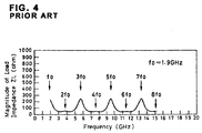
- the output terminal C is short-circuited at M-th order higher harmonics, and is released at N-th order higher harmonics, and in addition, the impedance found at the frequency f 0 is coincident with a load impedance of the conventional circuit, illustrated in Fig. 4.
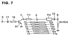
- Fig. 7 is a circuit diagram of an example of application of the circuit in accordance with the embodiment.
- the circuit in accordance with the embodiment is applied to a 1.9 GHz bandwidth amplification circuit including a heterojunction bipolar transistor (HBT).
- HBT heterojunction bipolar transistor
- the illustrated circuit is comprised of the circuit illustrated in Fig. 7, a heterojunction bipolar transistor Q1 having a collector electrically connected to the output terminal C and an emitter grounded, a third transmission line T0 electrically connected in series to a base of the transistor Q1 and having a length of ⁇ /4, a first coupling capacitor C1 electrically connected in series to the third transmission line T0 for prohibiting a direct current to flow therethrough, and a second capacitor electrically connected in series between the second transmission line T12 and the input terminal B of the resistor R 0 for prohibiting a direct current to flow therethrough.
- the transistor Q1 has a maximum oscillation frequency of 210 GHz, and has a sufficient power gain even in a seventh-order higher harmonics to a frequency of 1.9 GHz. This means that the circuit in accordance with the embodiment works well in the circuit illustrated in Fig. 7.
- Fig. 8A is a plan view of an example of a layout of a device in which the circuit in accordance with the embodiment is mounted, and Fig. 8B is a side view of the device.
- the illustrated device is comprised of a base block 31 composed of a metal, a first dielectric substrate 32 formed on the base block 31 in a first area, a second dielectric substrate 33 formed on the base block 31 in a second area, an input transmission line T0 formed on the first dielectric substrate 32, a first output transmission line T11 formed on the second dielectric substrate 33, a second output transmission line T12 formed on the second dielectric substrate 33 so that the second dielectric substrate 33 is straightly coupled at a connection point A with the first output transmission line T11, a first group of transmission lines T2 to T6 upwardly radially extending from the connection point A, a second group of transmission lines T2a to T6a downwardly radially extending from the connection point A, and a heterojunction bipolar transistor (HBT) Q1 between the first dielectric substrate 32 and the second dielectric substrate 33 and further between the input transmission line T0 and the first output transmission line T11.
- HBT heterojunction bipolar transistor
- the input transmission line T0 and the first and second output transmission lines T11 and T12 are all composed of a micro-strip electrical conductor.
- the arrangement of the first and second groups of transmission lines T2 to T6 and T2a to T6a is not to be limited to the arrangement illustrated in Fig. 8A. They may be arranged in any pattern, unless they extend from the same point.
- a frequency used is equal to or greater than 10 GHz, it would be preferable, from the standpoint of a circuit balance, to arrange two sets of the first group of transmission lines T2 to T6 and two sets of the second group of transmission lines T2a to T6a so that the two sets of the first group of transmission lines T2 to T6 are located in symmetry with the two sets of the second group of transmission lines T2a to T6a about the first and second output transmission lines T11 and T12.
- Fig. 9 is a graph showing waveforms of a current and a voltage measured at the output terminal C in the amplification circuit illustrated in Figs. 8A and 8B, when a power source voltage is 3.4 V. It is understood in view of Fig. 9 that the current waveform seldom overlaps the voltage waveform.
- Fig. 10 is a graph showing a relation between an input power and an output power, and a load power efficiency (PAE) of the circuit illustrated in Figs. 8A and 8B.
- the load power efficiency is quite high, specifically, about 88%.
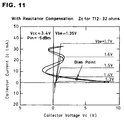
- Fig. 11 shows a dynamic load characteristic of the transistor Q1.
- the dynamic load characteristic of the transistor Q1 is quite different from that of a usual A-grade, B-grade or C-grade circuit. Specifically, when a voltage is applied to the transistor Q1, a current does not flow through the transistor Q1, and when a current flows through the transistor Q1, a voltage is not applied to the transistor Q1.
- the dynamic load line exists at the left of a rise-up point of the current-voltage static characteristic.
- a transistor used have a power gain of 10 dB or greater at a maximum order higher harmonics to be dealt with.
- Nf 0 it is necessary for Nf 0 to be within 1/3 of f max .
- the transistor Q1 may be a high electron mobility transistor (HEMT), a Si-MOSFET or a GaAs FET.
- HEMT high electron mobility transistor
- Si-MOSFET Si-MOSFET
- GaAs FET GaAs FET
Landscapes
- Engineering & Computer Science (AREA)
- Power Engineering (AREA)
- Microwave Amplifiers (AREA)
- Amplifiers (AREA)
- Control Of Motors That Do Not Use Commutators (AREA)
Abstract
Description
Claims (13)
- A circuit connected between an output terminal (C) of an amplification transistor and a resistor (R0) for dealing with higher harmonics included in an output signal transmitted from the amplification transistor, comprising:(a) a first transmission line (T11) having an input terminal electrically connected to the output terminal (C) of the amplification transistor, and having a length of λ/4 wherein λ indicates a wavelength of a fundamental harmonic; and(b) a first group of transmission lines (T2 to T6), including N transmission lines electrically connected in parallel with one another to an output terminal of the first transmission line (T11), wherein N is an integer equal to or greater than 1, each of the N transmission lines having a length L defined by the following equation:each of the N transmission lines having an open end,
characterized by(c) a second group of transmission lines (T2a to T6a), including N transmission lines electrically connected in parallel with one another to an output terminal of the first transmission line (T11), each of the N transmission lines having a length Lh defined by the following equation:each of the N transmission lines having an open end. - The circuit as set forth in claim 1, wherein the length Lh is defined by the following equation.
- The circuit as set forth in claim 1, further comprising a second transmission line (T12) having a length of λ/4 and located between an output terminal of the first transmission line (T11) and the resistor (R0).
- The circuit as set forth in claim 1, 2 or 3, wherein each of the first group of transmission lines (T2 to T6) is arranged in symmetry with each of the second group of transmission lines (T2a to T6a) in a lengthwise direction of the first transmission line (T11).
- The circuit as set forth in claim 1, 2 or 3, wherein each of the first group of transmission lines (T2 to T6) and each of the second group of transmission lines (T2a to T6a) extend from the same point.
- The circuit as set forth in claim 5, wherein each of the first group of transmission lines (T2 to T6) and each of the second group of transmission lines (T2a to T6a) radially extend from the same point.
- The circuit as set forth in claim 5, wherein each of the first group of transmission lines (T2 to T6) radially extend from the same point on one of sides of the first transmission line (T11) and each of the second group of transmission lines (T2a to T6a) radially extend from the same point on the other side of the first transmission line (T11).
- An amplification circuit comprising:(a) an amplification transistor (Q1); and(b) a circuit as defined in any one of claims 1 to 7, wherein the first transmission line (T11) receives an output signal transmitted from the amplification transistor (Q1).
- The amplification circuit as set forth in claim 8, wherein the amplification transistor (Q1) has a maximum oscillation frequency 3N or more times equal to or greater than a frequency of the fundamental harmonics.
- The amplification circuit as set forth in claim 8 or 9, further comprising a third transmission line (T0) having a wavelength of λ/4 and electrically connected in series to a base of the amplification transistor (Q1).
- The amplification circuit as set forth in claim 10, further comprising a first coupling capacitor (C1) located upstream of the third transmission line (T0) and electrically connected in series to the third transmission line (T0) for prohibiting a direct current to flow therethrough.
- The amplification circuit as set forth in claim 8 or 9, further comprising a second coupling capacitor (C2) located downstream of the second transmission line (T12) and electrically connected in series to the second transmission line (T12) for prohibiting a direct current to flow therethrough.
- The amplification circuit as set forth in claim 8 or 9, wherein the amplification transistor (Q1) is any one of a heterojunction bipolar transistor (HBT), a high electron mobility transistor (HEMT), a Si-MOSFET, and a GaAs FET.
Applications Claiming Priority (2)
| Application Number | Priority Date | Filing Date | Title |
|---|---|---|---|
| JP28498399A JP2001111362A (en) | 1999-10-06 | 1999-10-06 | Higher harmonic processing circuit and high power efficiency amplifier circuit using the same |
| JP28498399 | 1999-10-06 |
Publications (2)
| Publication Number | Publication Date |
|---|---|
| EP1091442A2 true EP1091442A2 (en) | 2001-04-11 |
| EP1091442A3 EP1091442A3 (en) | 2002-06-26 |
Family
ID=17685625
Family Applications (1)
| Application Number | Title | Priority Date | Filing Date |
|---|---|---|---|
| EP00121758A Withdrawn EP1091442A3 (en) | 1999-10-06 | 2000-10-05 | Circuit for dealing with higher harmonics and circuit for amplifying power efficiency |
Country Status (3)
| Country | Link |
|---|---|
| US (1) | US6396348B1 (en) |
| EP (1) | EP1091442A3 (en) |
| JP (1) | JP2001111362A (en) |
Cited By (4)
| Publication number | Priority date | Publication date | Assignee | Title |
|---|---|---|---|---|
| EP2302731A1 (en) * | 2009-09-18 | 2011-03-30 | Fujitsu Limited | Filter and amplifying circuit |
| EP2058943A4 (en) * | 2006-08-08 | 2011-08-10 | Nat University Corp The University Of Electro Comm | HARMONIC PROCESSING CIRCUIT AND AMPLIFICATION CIRCUIT USING THE CIRCUIT FOR PROCESSING |
| EP2584698A4 (en) * | 2010-06-21 | 2013-10-16 | Panasonic Corp | HIGH FREQUENCY AMPLIFIER CIRCUIT |
| EP2752990A4 (en) * | 2011-08-29 | 2015-07-08 | Univ Electro Communications | HIGH PERFORMANCE POWER AMPLIFIER |
Families Citing this family (21)
| Publication number | Priority date | Publication date | Assignee | Title |
|---|---|---|---|---|
| ATE417410T1 (en) * | 2004-11-25 | 2008-12-15 | Murata Manufacturing Co | HIGH FREQUENCY SWITCHING MODULE |
| US7288995B2 (en) * | 2005-06-15 | 2007-10-30 | Nokia Corporation | Power amplifier of a transmitter |
| JP5085179B2 (en) | 2007-04-12 | 2012-11-28 | 株式会社東芝 | Class F amplifier circuit |
| WO2009019795A1 (en) * | 2007-08-07 | 2009-02-12 | Fujitsu Limited | Reactance varying device |
| JP2009094805A (en) * | 2007-10-09 | 2009-04-30 | Sumitomo Electric Ind Ltd | amplifier |
| JP2009094921A (en) | 2007-10-11 | 2009-04-30 | Mitsubishi Electric Corp | High frequency power amplifier |
| JP5453120B2 (en) * | 2009-01-30 | 2014-03-26 | 株式会社Nttドコモ | Multiband matching circuit and multiband power amplifier |
| WO2010096582A2 (en) | 2009-02-18 | 2010-08-26 | Rayspan Corporation | Metamaterial power amplifier systems |
| JP5408616B2 (en) * | 2009-08-31 | 2014-02-05 | 国立大学法人電気通信大学 | Amplifier circuit |
| JP5762690B2 (en) * | 2009-10-02 | 2015-08-12 | 富士通株式会社 | Filter and transmitter / receiver |
| US20120038432A1 (en) * | 2010-07-14 | 2012-02-16 | Andrews M Scott | Wideband impedance matching of power amplifiers in a planar waveguide |
| WO2013001711A1 (en) | 2011-06-28 | 2013-01-03 | パナソニック株式会社 | High-frequency power amplifier |
| JP6189881B2 (en) | 2015-01-27 | 2017-08-30 | 株式会社東芝 | High frequency semiconductor amplifier |
| JP6189880B2 (en) | 2015-01-27 | 2017-08-30 | 株式会社東芝 | High frequency semiconductor amplifier |
| JP6190399B2 (en) | 2015-01-28 | 2017-08-30 | 株式会社東芝 | High frequency semiconductor amplifier |
| JP6109868B2 (en) | 2015-03-06 | 2017-04-05 | 株式会社東芝 | High frequency amplifier |
| WO2016199797A1 (en) * | 2015-06-09 | 2016-12-15 | 国立大学法人電気通信大学 | Multiband amplifier and dual-band amplifier |
| JP2017041800A (en) * | 2015-08-20 | 2017-02-23 | 学校法人 芝浦工業大学 | Harmonic processing circuit and class F amplifier circuit using the same |
| CN108736838A (en) * | 2017-04-16 | 2018-11-02 | 天津大学(青岛)海洋工程研究院有限公司 | A kind of novel F classes power amplifier match circuit that higher hamonic wave is controllable |
| US11502653B2 (en) * | 2019-11-22 | 2022-11-15 | Skyworks Solutions, Inc. | Metamaterial based power amplifier module |
| JP7487154B2 (en) * | 2021-08-10 | 2024-05-20 | 株式会社京三製作所 | High Frequency Amplifier |
Family Cites Families (7)
| Publication number | Priority date | Publication date | Assignee | Title |
|---|---|---|---|---|
| JPH02152302A (en) * | 1988-12-02 | 1990-06-12 | Fujitsu Ltd | Double wave blocking circuit |
| JP3424940B2 (en) | 1992-03-09 | 2003-07-07 | 株式会社日本製鋼所 | Evacuation method and apparatus using turbo molecular pump |
| JPH0738548B2 (en) * | 1993-01-07 | 1995-04-26 | 日本電気株式会社 | Power matching circuit |
| JP2513146B2 (en) | 1993-09-20 | 1996-07-03 | 日本電気株式会社 | High efficiency amplifier circuit |
| JP2616464B2 (en) | 1994-10-31 | 1997-06-04 | 日本電気株式会社 | High efficiency power amplifier circuit |
| JPH1188459A (en) | 1997-09-12 | 1999-03-30 | Hitachi Ltd | Serial bus connection system |
| JP3560464B2 (en) * | 1998-03-11 | 2004-09-02 | アルプス電気株式会社 | Harmonic suppression circuit |
-
1999
- 1999-10-06 JP JP28498399A patent/JP2001111362A/en active Pending
-
2000
- 2000-10-05 EP EP00121758A patent/EP1091442A3/en not_active Withdrawn
- 2000-10-05 US US09/679,620 patent/US6396348B1/en not_active Expired - Fee Related
Cited By (5)
| Publication number | Priority date | Publication date | Assignee | Title |
|---|---|---|---|---|
| EP2058943A4 (en) * | 2006-08-08 | 2011-08-10 | Nat University Corp The University Of Electro Comm | HARMONIC PROCESSING CIRCUIT AND AMPLIFICATION CIRCUIT USING THE CIRCUIT FOR PROCESSING |
| EP2302731A1 (en) * | 2009-09-18 | 2011-03-30 | Fujitsu Limited | Filter and amplifying circuit |
| EP2584698A4 (en) * | 2010-06-21 | 2013-10-16 | Panasonic Corp | HIGH FREQUENCY AMPLIFIER CIRCUIT |
| EP2752990A4 (en) * | 2011-08-29 | 2015-07-08 | Univ Electro Communications | HIGH PERFORMANCE POWER AMPLIFIER |
| US9257948B2 (en) | 2011-08-29 | 2016-02-09 | The University Of Electro-Communications | High efficiency power amplifier |
Also Published As
| Publication number | Publication date |
|---|---|
| EP1091442A3 (en) | 2002-06-26 |
| US6396348B1 (en) | 2002-05-28 |
| JP2001111362A (en) | 2001-04-20 |
Similar Documents
| Publication | Publication Date | Title |
|---|---|---|
| EP1091442A2 (en) | Circuit for dealing with higher harmonics and circuit for amplifying power efficiency | |
| US4717884A (en) | High efficiency RF power amplifier | |
| JP4476534B2 (en) | Amplifier circuit | |
| US6577199B2 (en) | Harmonic matching network for a saturated amplifier | |
| US6414545B1 (en) | Predistortion to improve linearity of an amplifier | |
| KR101052180B1 (en) | Harmonic Processing Circuit and Amplifier Circuit Using the Same | |
| US6614311B2 (en) | Micro-wave power amplifier | |
| US6614308B2 (en) | Multi-stage, high frequency, high power signal amplifier | |
| US5300895A (en) | Method for terminating harmonics of transistors | |
| JP2008263438A (en) | Class F amplifier circuit | |
| CN108023552B (en) | A radio frequency power amplifier system for microwave wireless power transmission device | |
| EP1201028B1 (en) | Transistor amplifier having reduced parasitic oscillations | |
| JPH0794974A (en) | Highly efficient amplifier circuit | |
| GB2211688A (en) | Bias voltage supply circuit for distributed fet amplifier | |
| US7385450B2 (en) | Bias circuit | |
| US6946934B2 (en) | Transmission line and semiconductor integrated circuit device | |
| CA1210093A (en) | High frequency amplifier | |
| US7135931B2 (en) | Negative conductance power amplifier | |
| US20040061565A1 (en) | Integrated circuit oscillator | |
| JPH04326206A (en) | Power amplifier | |
| KR101678132B1 (en) | Distributed power amplifier with active matching | |
| JP2616464B2 (en) | High efficiency power amplifier circuit | |
| US7242253B2 (en) | Low noise amplifier | |
| JP6837602B2 (en) | Distributed amplifier | |
| US7492230B2 (en) | Method and apparatus for effecting high-frequency amplification or oscillation |
Legal Events
| Date | Code | Title | Description |
|---|---|---|---|
| PUAI | Public reference made under article 153(3) epc to a published international application that has entered the european phase |
Free format text: ORIGINAL CODE: 0009012 |
|
| AK | Designated contracting states |
Kind code of ref document: A2 Designated state(s): AT BE CH CY DE DK ES FI FR GB GR IE IT LI LU MC NL PT SE |
|
| AX | Request for extension of the european patent |
Free format text: AL;LT;LV;MK;RO;SI |
|
| PUAL | Search report despatched |
Free format text: ORIGINAL CODE: 0009013 |
|
| AK | Designated contracting states |
Kind code of ref document: A3 Designated state(s): AT BE CH CY DE DK ES FI FR GB GR IE IT LI LU MC NL PT SE |
|
| AX | Request for extension of the european patent |
Free format text: AL;LT;LV;MK;RO;SI |
|
| 17P | Request for examination filed |
Effective date: 20020620 |
|
| AKX | Designation fees paid |
Designated state(s): DE FR GB SE |
|
| 17Q | First examination report despatched |
Effective date: 20061103 |
|
| STAA | Information on the status of an ep patent application or granted ep patent |
Free format text: STATUS: THE APPLICATION HAS BEEN WITHDRAWN |
|
| 18W | Application withdrawn |
Effective date: 20061228 |