EP1091416A2 - GaAs MOSFET having low capacitance and on-resistance and method of manufacturing the same - Google Patents
GaAs MOSFET having low capacitance and on-resistance and method of manufacturing the same Download PDFInfo
- Publication number
- EP1091416A2 EP1091416A2 EP00308684A EP00308684A EP1091416A2 EP 1091416 A2 EP1091416 A2 EP 1091416A2 EP 00308684 A EP00308684 A EP 00308684A EP 00308684 A EP00308684 A EP 00308684A EP 1091416 A2 EP1091416 A2 EP 1091416A2
- Authority
- EP
- European Patent Office
- Prior art keywords
- layer
- gate
- epitaxial layer
- recited
- mosfet
- Prior art date
- Legal status (The legal status is an assumption and is not a legal conclusion. Google has not performed a legal analysis and makes no representation as to the accuracy of the status listed.)
- Granted
Links
Images


Classifications
-
- H—ELECTRICITY
- H10—SEMICONDUCTOR DEVICES; ELECTRIC SOLID-STATE DEVICES NOT OTHERWISE PROVIDED FOR
- H10D—INORGANIC ELECTRIC SEMICONDUCTOR DEVICES
- H10D30/00—Field-effect transistors [FET]
- H10D30/01—Manufacture or treatment
- H10D30/021—Manufacture or treatment of FETs having insulated gates [IGFET]
-
- H—ELECTRICITY
- H10—SEMICONDUCTOR DEVICES; ELECTRIC SOLID-STATE DEVICES NOT OTHERWISE PROVIDED FOR
- H10D—INORGANIC ELECTRIC SEMICONDUCTOR DEVICES
- H10D30/00—Field-effect transistors [FET]
- H10D30/60—Insulated-gate field-effect transistors [IGFET]
- H10D30/601—Insulated-gate field-effect transistors [IGFET] having lightly-doped drain or source extensions, e.g. LDD IGFETs or DDD IGFETs
- H10D30/603—Insulated-gate field-effect transistors [IGFET] having lightly-doped drain or source extensions, e.g. LDD IGFETs or DDD IGFETs having asymmetry in the channel direction, e.g. lateral high-voltage MISFETs having drain offset region or extended drain IGFETs [EDMOS]
-
- H—ELECTRICITY
- H10—SEMICONDUCTOR DEVICES; ELECTRIC SOLID-STATE DEVICES NOT OTHERWISE PROVIDED FOR
- H10D—INORGANIC ELECTRIC SEMICONDUCTOR DEVICES
- H10D62/00—Semiconductor bodies, or regions thereof, of devices having potential barriers
- H10D62/80—Semiconductor bodies, or regions thereof, of devices having potential barriers characterised by the materials
- H10D62/85—Semiconductor bodies, or regions thereof, of devices having potential barriers characterised by the materials being Group III-V materials, e.g. GaAs
Definitions
- the present invention is directed, in general, to semiconductor fabrication and, more specifically, to a gallium arsenide metal-oxide semiconductor field effect transistor (GaAs MOSFET) having low capacitance and on-resistance and method of manufacturing the same.
- GaAs MOSFET gallium arsenide metal-oxide semiconductor field effect transistor
- Integrated circuits are no exception and large demand for improved functionality and enhanced performance continues to increase.
- the IC industry continues to decrease the size of component devices to place more circuits in the same amount of space.
- structures have diminished from 1.2 m gate areas to gate areas of 0.25 m and promise to become even smaller in the future.
- Channel resistance appears to be limited by the characteristics of the gate oxide interface. High temperature annealing steps produce a rough interface between the oxide and underlying doped regions. Much effort has been expended in the search for processes that reduce the interface irregularities. Also, gate oxide materials having inherently better interface characteristics have been sought. Such efforts have met with moderate success as evidenced by the limitations of current state-of-the-art devices.
- the present invention provides a MOSFET, a method of manufacturing the MOSFET and a power supply incorporating at least one such MOSFET.
- the MOSFET includes: (1) a substrate having an epitaxial layer underlying a gate oxide layer, a portion of the epitaxial layer being a gate region of the MOSFET, (2) an N-type drift region located in the epitaxial layer laterally proximate the gate region and (3) source and drain regions located in the epitaxial layer and laterally straddling the gate and drift regions.
- the term "laterally straddling" means being located on both sides of.
- the present invention therefore introduces the broad concept of structuring a MOSFET laterally, such that its channel resistance, and therefore its input and output capacitances and on-resistance, are reduced.
- the substrate employed to fabricate a MOSFET according to the principles of the present invention comprises gallium arsenide.
- the epitaxial layer is beryllium-doped.
- the epitaxial layer is beryllium-doped.
- P-type or N-type dopants fall within the broad scope of the present invention.
- the gate oxide layer comprises gallium III oxide.
- the gate oxide layer is formed by way of electron beam evaporation from a single-crystal source.
- the drift, drain and source regions comprise a silicon dopant.
- a silicon dopant Those skilled in the pertinent art will understand that other conventional N-type dopants fall within the broad scope of the present invention.
- the MOSFET further includes an N layer located in the epitaxial layer and between the gate region and the gate oxide layer.
- the N layer is preferably doped such that, at zero bias, a first depletion region within the N layer proximate the gate region contacts a second depletion region within the N layer proximate the gate oxide layer.
- the power conversion circuit 100 includes an isolation transformer having a primary winding 110 and a secondary winding 120. Coupled to the primary winding 110 is a primary-side power switch 130. Such a circuit also includes secondary-side power switches 140 coupled to the secondary winding and an output inductor 150 coupled to the at least one of the secondary-side power switches 140. An output capacitor 160 is coupled to the output inductor 150 across an output of the power supply 170.
- the power supply circuit 100 also has a control drive 180, coupled to the primary-side power switch 130, for providing control signals to the power switch 130.
- FIGURE 2 illustrated is a cross-sectional view of a prior art power switching device 200 that may be used as the primary-side power switch 130 or one or both of the secondary-side power switches 140 in the power converter circuit 100 of FIGURE 1.
- the device 200 is a vertically structured metal-oxide semiconductor device (VDMOS).
- the device 200 includes a drain contact layer 210 over which a silicon substrate 220 is formed.
- An N-drift region 230 is then formed in the silicon substrate according to conventional methods, followed by formation of P-doped regions 240 to define a gate.
- P-doped regions 240 On either side of the gate and within the P-doped regions 240, N+ regions 250 are formed.
- a gate oxide layer 260 is deposited over the exposed surfaces of the N+ regions 250, the P-doped regions 240, and the N-drift region 230.
- the gate oxide layer 260 is patterned and the desired source contacts 270 are formed connecting to the N+ regions 250.
- a gate contact layer 280 is deposited over the gate oxide layer 260 and at least partially overlapping the P-doped layers 240.
- the methods and materials for forming the various layers and regions of such a VDMOS device are well-known to those skilled in the art.
- FIGUREs 3a-d illustrated are cross-sectional views of an exemplary embodiment of a power switching device 300 constructed according to the principles of the present invention.
- the power switching device 300 may replace the prior art power switch 130 on the primary winding of the power conversion circuit 100 of FIGURE 1.
- the device 300 may replace one or both of the secondary-side power switches 140.
- both the primary- and secondary-side power switches may be the switching device 300.
- the power switching device 300 of the present invention is formed on a substrate which is preferably a semi-insulating gallium arsenide (GaAs) substrate.
- a P-type layer 320 is formed on the substrate 310. Any material that is currently known or subsequently found to be suitable for forming P-doped layers is envisioned by the current invention.
- the P-type layer 320 is formed by doping the substrate 310 with beryllium.
- the layer 320 is formed epitaxially. The thickness of the P-type layer 320 will vary according to design specifications. Other methods for forming such P-type layers are known to those skilled in the art may also be used to form the P-type layer 320.
- a photoresist, implant mask is used to convert portions of the P-type layer 320 to N-drift regions 330.
- the N-drift regions 330 may be formed by conventional methods. In a particularly useful embodiment, the N-drift regions 330 are formed by silicon implantation. The N-drift regions 330 are formed to isolate a gate region 325 of the unmodified P-type region that is laterally bordered by the N-drift region. Portions of the N-drift regions 330 are then converted to N+ source and drain regions 340 and 350, according to conventional methods. The source and drain regions 340 and 350 laterally straddle the gate region 325 and an unmodified portion of the N-drift region 330.
- the source and drain regions are formed by silicon implantation and activation at 850°C. While the source and drain regions 340 and 350 may be formed by silicon implantation, one skilled in the art will appreciate that other conventional or later-discovered methods for forming N+ source and drain regions may be used. While the embodiment described calls for the source and drain regions 340 and 350 to be formed in the same process step, one skilled in the art will also understand that the source and drain regions 340 and 350 may be formed in separate steps.
- a gate oxide layer 360 is deposited.
- Gate oxide deposition is performed in a multi-chamber molecular beam epitaxy (MBE) system that includes a solid source GaAs-based III-V chamber and an oxide decomposition chamber with a background pressure below 10 -9 torr.
- MBE molecular beam epitaxy
- native oxide impurities are thermally desorbed at substrate temperatures in the range of 580°C to 600°C in the III-V chamber under an arsenic (As) over-pressure.
- As arsenic
- the desired thickness of gate oxide layer 360 is deposited under ultra-high vacuum (10 -10 torr) conditions in the deposition chamber.
- the thickness of the gate oxide layer may vary according to design specifications; however, in one embodiment, the desired thickness is approximately 20 nm.
- the gate oxide layer 360 is deposited as substantially gallium (III) oxide, Ga 2 O 3 at a substrate temperature of approximately 535°C by electron-beam evaporation from a single- crystal source of Ga 5 Gd 3 O 12 . Further details of some acceptable gate oxide layer deposition parameters can be found in U.S. Patent No. 5,821,171 to Hong, et . al ., incorporated herein by reference.
- the gate oxide layer 360 is then patterned so that source and drain contact regions 370 and 380 may be formed.
- a gate metal region 390 is formed over at least a portion of the gate oxide layer 360.
- Materials for the gate metal and contact metals may be any material currently known or subsequently discovered to be suitable for such purposes.
- the lateral structure substantially eliminates substrate resistance. Also, drift resistance which limits the performance in VDMOS prior art devices is substantially eliminated. Therefore the present invention is especially well-suited for deep-level integration.
- the GaAs substrate material provides a higher breakdown field that is 1.5 times higher than that of silicon. Electron mobility in the GaAs substrate is 5 times greater than in silicon. Therefore, the device according to the present invention shows approximately a 10-fold reduction in drift resistance compared to prior art VDMOS switches.
- the total resistance of power switches constructed according to the principles of the present invention will have less than one-tenth of the total resistance of prior art VDMOS devices.
- the power conversion switch just described provides a substantial improvement in operating characteristics when incorporated into a power conversion circuit such as circuit 100. Such switch is particularly useful where low voltage and high current are required. For example, in an 8V output supply operating at 50 amps, prior art MOSFET switches operate at about 82% efficiency. If the prior art switches are replaced with those constructed according to the principles of the present invention, the on-resistance is reduced by a factor of about 6 and the efficiency increases to around 92%. Such a level of operating efficiency is extremely difficult to achieve with prior art silicon-based power conversion switches.
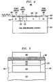
- FIGURE 4 illustrated is an embodiment 400 of the present invention that further incorporates an N-type layer underlying the gate oxide in the gate region 420.
- the GaAs substrate 410, gate region 420, N-drift regions, and laterally straddling N+ source and drain regions 440 and 450, respectively, are formed in the manner described in conjunction with FIGURE 3.
- an upper portion of the gate region 420 is then doped to form a thin N-type layer 425 over the unmodified portion of the gate region 420.
- Such processing steps may be performed by methods known to those skilled in the art.
- the gate oxide layer 460, source 470 and drain 480 contacts, and the gate contact 490 may be formed in the manner described above with respect to FIGURE 3.
- the N-type layer 425 is advantageously (but not necessarily) designed to have a thickness and dopant concentration such that, at zero bias, the first depletion region 426 within the N-layer 425 contacts the underlying second depletion region 427. Further, the surface roughness of the N-type layer 425 should be less than the width of depletion region 426. In one embodiment, the surface roughness is approximately 5 nm.
- the N-layer 425 has an N-dopant concentration of 2 x 10 17 cm -3 inducing the depletion region 426 to have a width of 100 nm.
- Such characteristics should cause the device of FIGUREs 4 and 5 to be a normally-off device.
- a positive bias is applied to the device, an accumulation channel is formed and the N-layer 425 increases the effective channel mobility, concomitantly reducing the channel resistance of the device dramatically.
- the reduced channel resistance of the device allows the device of the present invention to be used in low voltage applications where the prior art is inadequate.
- the N-layer 425 has been described with respect to the power converter switches of the present invention, such a layer may be used in any other GaAs MOSFET structure as a way to increase channel mobility.
Landscapes
- Insulated Gate Type Field-Effect Transistor (AREA)
- Junction Field-Effect Transistors (AREA)
Abstract
Description

Claims (21)
- A metal-oxide semiconductor field effect transistor (MOSFET), comprising:a substrate having an epitaxial layer underlying a gate oxide layer, a portion of the epitaxial layer being a gate region of the MOSFET;an N-type drift region located in the epitaxial layer laterally proximate the gate region; andsource and drain regions located in the epitaxial layer and laterally straddling the gate and drift regions.
- The MOSFET as recited in Claim 1 wherein the substrate comprises gallium arsenide.
- The MOSFET as recited in Claim 1 wherein the epitaxial layer is beryllium-doped.
- The MOSFET as recited in Claim 1 wherein the gate oxide layer comprises gallium III oxide.
- The MOSFET as recited in Claim 1 wherein the drift region comprises a silicon dopant.
- The MOSFET as recited in Claim 1 wherein the source and drain regions each comprise a silicon dopant.
- The MOSFET as recited in Claim 1 further comprising an N layer located in the epitaxial layer and between the gate region and the gate oxide layer, the N layer being doped such that, at zero bias, a first depletion region within the N layer proximate the gate region contacts a second depletion region within the N layer proximate the gate oxide layer.
- A method of manufacturing a metal-oxide semiconductor field effect transistor (MOSFET), comprising:forming an epitaxial layer over a substrate, a portion of the epitaxial layer being a gate region of the MOSFET;forming a gate oxide layer over the epitaxial layer;forming an N-type drift region in the epitaxial layer laterally proximate the gate region; andforming source and drain regions in the epitaxial layer, the source and drain regions laterally straddling the gate and drift regions.
- The method as recited in Claim 8 wherein the substrate comprises gallium arsenide.
- The method as recited in Claim 8 wherein the forming the epitaxial layer comprises doping a portion of the substrate with beryllium.
- The method as recited in Claim 8 wherein the forming the gate oxide layer comprises employing electron beam evaporation from a single-crystal source.
- The method as recited in Claim 8 wherein the forming the drift region comprises doping a portion of the epitaxial layer with silicon.
- The method as recited in Claim 8 wherein the forming the source and drain regions comprises doping portions of the epitaxial layer with silicon.
- The method as recited in Claim 8 further comprising:forming an N layer in the epitaxial layer and between the gate region and the gate oxide layer; anddoping the N layer such that, at zero bias, a first depletion region within the N layer proximate the gate region contacts a second depletion region within the N layer proximate the gate oxide layer.
- A power supply, comprising:an isolation transformer having primary and secondary windings;a primary-side power switch, coupled to the primary winding;at least one secondary-side power switch coupled to the secondary winding;an output inductor coupled to the at least one secondary-side power switch;an output capacitor coupled to the output inductor and across an output of the power supply; anda control drive, coupled to the primary-side power switch, that provides control signals thereto, the primary-side power switch being a metal-oxide semiconductor field effect transistor (MOSFET), including:a substrate having an epitaxial layer underlying a gate oxide layer, a portion of the epitaxial layer being a gate region of the MOSFET,an N-type drift region located in the epitaxial layer laterally proximate the gate region, andsource and drain regions located in the epitaxial layer and laterally straddling the gate and drift regions.
- The power supply as recited in Claim 15 wherein the substrate comprises gallium arsenide.
- The power supply as recited in Claim 15 wherein the epitaxial layer is beryllium-doped.
- The power supply as recited in Claim 15 wherein the gate oxide layer comprises gallium III oxide.
- The power supply as recited in Claim 15 wherein the drift region comprises a silicon dopant.
- The power supply as recited in Claim 15 wherein the source and drain regions each comprise a silicon dopant.
- The power supply as recited in Claim 15 further comprising an N layer located in the epitaxial layer and between the gate region and the gate oxide layer, the N layer being doped such that, at zero bias, a first depletion region within the N layer proximate the gate region contacts a second depletion region within the N layer proximate the gate oxide layer.
Applications Claiming Priority (2)
| Application Number | Priority Date | Filing Date | Title |
|---|---|---|---|
| US412847 | 1999-10-06 | ||
| US09/412,847 US6369408B1 (en) | 1999-10-06 | 1999-10-06 | GaAs MOSFET having low capacitance and on-resistance and method of manufacturing the same |
Publications (3)
| Publication Number | Publication Date |
|---|---|
| EP1091416A2 true EP1091416A2 (en) | 2001-04-11 |
| EP1091416A3 EP1091416A3 (en) | 2003-03-05 |
| EP1091416B1 EP1091416B1 (en) | 2008-12-31 |
Family
ID=23634740
Family Applications (1)
| Application Number | Title | Priority Date | Filing Date |
|---|---|---|---|
| EP00308684A Expired - Lifetime EP1091416B1 (en) | 1999-10-06 | 2000-10-03 | GaAs MOSFET having low capacitance and on-resistance |
Country Status (4)
| Country | Link |
|---|---|
| US (2) | US6369408B1 (en) |
| EP (1) | EP1091416B1 (en) |
| JP (1) | JP4558911B2 (en) |
| DE (1) | DE60041233D1 (en) |
Families Citing this family (6)
| Publication number | Priority date | Publication date | Assignee | Title |
|---|---|---|---|---|
| US7038295B2 (en) * | 2003-07-18 | 2006-05-02 | Semiconductor Components Industries, L.L.C. | DC/DC converter with depletion mode compound semiconductor field effect transistor switching device |
| US7429506B2 (en) * | 2005-09-27 | 2008-09-30 | Freescale Semiconductor, Inc. | Process of making a III-V compound semiconductor heterostructure MOSFET |
| US20070090405A1 (en) * | 2005-09-27 | 2007-04-26 | Matthias Passlack | Charge compensated dielectric layer structure and method of making the same |
| US7432565B2 (en) * | 2005-09-27 | 2008-10-07 | Freescale Semiconductor, Inc. | III-V compound semiconductor heterostructure MOSFET device |
| US7682912B2 (en) | 2006-10-31 | 2010-03-23 | Freescale Semiconductor, Inc. | III-V compound semiconductor device with a surface layer in access regions having charge of polarity opposite to channel charge and method of making the same |
| US20100088855A1 (en) * | 2008-10-14 | 2010-04-15 | Magna Mirrors Of America, Inc. | Vehicle door handle assembly |
Family Cites Families (14)
| Publication number | Priority date | Publication date | Assignee | Title |
|---|---|---|---|---|
| US3890215A (en) * | 1974-02-08 | 1975-06-17 | Bell Telephone Labor Inc | Electrochemical thinning of semiconductor devices |
| JPS5587483A (en) * | 1978-12-25 | 1980-07-02 | Fujitsu Ltd | Mis type semiconductor device |
| US4805003A (en) * | 1987-11-10 | 1989-02-14 | Motorola Inc. | GaAs MESFET |
| AU2864692A (en) * | 1989-03-02 | 1994-02-14 | Thunderbird Technologies, Inc. | Fermi threshold silicon-on-insulator field effect transistor |
| US5132753A (en) * | 1990-03-23 | 1992-07-21 | Siliconix Incorporated | Optimization of BV and RDS-on by graded doping in LDD and other high voltage ICs |
| EP0497427B1 (en) * | 1991-02-01 | 1996-04-10 | Koninklijke Philips Electronics N.V. | Semiconductor device for high voltage application and method of making the same |
| JP2746482B2 (en) * | 1991-02-14 | 1998-05-06 | 三菱電機株式会社 | Field effect transistor and method for manufacturing the same |
| US5543654A (en) * | 1992-01-28 | 1996-08-06 | Thunderbird Technologies, Inc. | Contoured-tub fermi-threshold field effect transistor and method of forming same |
| US5357130A (en) * | 1992-07-24 | 1994-10-18 | Hughes Aircraft Company | Low-noise cryogenic MOSFET |
| US5406096A (en) * | 1993-02-22 | 1995-04-11 | Texas Instruments Incorporated | Device and method for high performance high voltage operation |
| US5303138A (en) * | 1993-04-29 | 1994-04-12 | At&T Bell Laboratories | Low loss synchronous rectifier for application to clamped-mode power converters |
| US5550089A (en) * | 1994-03-23 | 1996-08-27 | Lucent Technologies Inc. | Gallium oxide coatings for optoelectronic devices using electron beam evaporation of a high purity single crystal Gd3 Ga5 O12 source. |
| TW360982B (en) * | 1996-01-26 | 1999-06-11 | Matsushita Electric Works Ltd | Thin film transistor of silicon-on-insulator type |
| US5781420A (en) * | 1996-07-18 | 1998-07-14 | International Power Devices, Inc. | Single ended forward DC-to-DC converter providing enhanced resetting for synchronous rectification |
-
1999
- 1999-10-06 US US09/412,847 patent/US6369408B1/en not_active Expired - Lifetime
-
2000
- 2000-10-03 EP EP00308684A patent/EP1091416B1/en not_active Expired - Lifetime
- 2000-10-03 DE DE60041233T patent/DE60041233D1/en not_active Expired - Lifetime
- 2000-10-06 JP JP2000307041A patent/JP4558911B2/en not_active Expired - Lifetime
-
2001
- 2001-08-10 US US09/927,194 patent/US6682962B2/en not_active Expired - Fee Related
Also Published As
| Publication number | Publication date |
|---|---|
| US6682962B2 (en) | 2004-01-27 |
| DE60041233D1 (en) | 2009-02-12 |
| US6369408B1 (en) | 2002-04-09 |
| JP4558911B2 (en) | 2010-10-06 |
| EP1091416B1 (en) | 2008-12-31 |
| EP1091416A3 (en) | 2003-03-05 |
| US20010050393A1 (en) | 2001-12-13 |
| JP2001189452A (en) | 2001-07-10 |
Similar Documents
| Publication | Publication Date | Title |
|---|---|---|
| EP4336563A1 (en) | Gan-based hemt structure having multiple threshold voltages, and preparation method therefor and application thereof | |
| KR101954471B1 (en) | Method for growing iii-v epitaxial layers and semiconductor structure | |
| EP3008759B1 (en) | Cascode structures with gan cap layers | |
| US9252258B2 (en) | CMOS compatible method for manufacturing a HEMT device and the HEMT device thereof | |
| KR101674274B1 (en) | Method for growing iii-v epitaxial layers | |
| US20030235974A1 (en) | Advanced RF enhancement-mode FETs with improved gate properties | |
| US6518138B2 (en) | Method of forming Self-aligned lateral DMOS with spacer drift region | |
| US11670502B2 (en) | SiC MOSFET and method for manufacturing the same | |
| WO2016144263A1 (en) | Self-aligning source, drain and gate process for iii-v nitride mishemts | |
| WO2022101736A1 (en) | Multi-threshold voltage gallium nitride high electron mobility transistor | |
| US6369408B1 (en) | GaAs MOSFET having low capacitance and on-resistance and method of manufacturing the same | |
| US6903373B1 (en) | SiC MOSFET for use as a power switch and a method of manufacturing the same | |
| US20220384641A1 (en) | Method for manufacturing semiconductor device, and semiconductor device | |
| CN119767724B (en) | GaN-based enhanced HEMT device structure and manufacturing method thereof | |
| WO2022101740A1 (en) | Monolithic integration of enhancement-mode and depletion-mode galium nitride high electron mobility transistors | |
| EP4439677A1 (en) | Hemt device having an improved gate structure and manufacturing process thereof | |
| CN119008625A (en) | Enhanced SiC substrate GaN power electronic device | |
| CA3209196A1 (en) | Gan-based hemt structure having multithreshold voltage, and preparation method and application therefor | |
| KR102739884B1 (en) | Structure of GaN power device with low gate capacitance and its fabrication method | |
| KR102750323B1 (en) | Structure of GaN device for high voltage robustness and its fabrication method | |
| KR102743228B1 (en) | Structure of GaN device with double self-align gate and its fabrication method | |
| KR20230000816A (en) | Structure of GaN power device consisting of self-aligned n-p junction gate and its fabrication method | |
| KR20220096786A (en) | Schottky barrier diode and method for manufacturing the same | |
| US20260068266A1 (en) | Scalable iii-n devices with threshold voltage control | |
| KR20250094986A (en) | Semiconductor device and method for manufacturing the same |
Legal Events
| Date | Code | Title | Description |
|---|---|---|---|
| PUAI | Public reference made under article 153(3) epc to a published international application that has entered the european phase |
Free format text: ORIGINAL CODE: 0009012 |
|
| AK | Designated contracting states |
Kind code of ref document: A2 Designated state(s): AT BE CH CY DE DK ES FI FR GB GR IE IT LI LU MC NL PT SE |
|
| AX | Request for extension of the european patent |
Free format text: AL;LT;LV;MK;RO;SI |
|
| PUAL | Search report despatched |
Free format text: ORIGINAL CODE: 0009013 |
|
| AK | Designated contracting states |
Kind code of ref document: A3 Designated state(s): AT BE CH CY DE DK ES FI FR GB GR IE IT LI LU MC NL PT SE |
|
| AX | Request for extension of the european patent |
Extension state: AL LT LV MK RO SI |
|
| 17P | Request for examination filed |
Effective date: 20030828 |
|
| AKX | Designation fees paid |
Designated state(s): DE FR GB |
|
| 17Q | First examination report despatched |
Effective date: 20031119 |
|
| RIC1 | Information provided on ipc code assigned before grant |
Ipc: H01L 29/78 20060101AFI20080610BHEP |
|
| RTI1 | Title (correction) |
Free format text: GAAS MOSFET HAVING LOW CAPACITANCE AND ON-RESISTANCE |
|
| GRAP | Despatch of communication of intention to grant a patent |
Free format text: ORIGINAL CODE: EPIDOSNIGR1 |
|
| GRAS | Grant fee paid |
Free format text: ORIGINAL CODE: EPIDOSNIGR3 |
|
| GRAA | (expected) grant |
Free format text: ORIGINAL CODE: 0009210 |
|
| AK | Designated contracting states |
Kind code of ref document: B1 Designated state(s): DE FR GB |
|
| REG | Reference to a national code |
Ref country code: GB Ref legal event code: FG4D |
|
| REF | Corresponds to: |
Ref document number: 60041233 Country of ref document: DE Date of ref document: 20090212 Kind code of ref document: P |
|
| RAP4 | Party data changed (patent owner data changed or rights of a patent transferred) |
Owner name: LUCENT TECHNOLOGIES INC. |
|
| PLBE | No opposition filed within time limit |
Free format text: ORIGINAL CODE: 0009261 |
|
| STAA | Information on the status of an ep patent application or granted ep patent |
Free format text: STATUS: NO OPPOSITION FILED WITHIN TIME LIMIT |
|
| 26N | No opposition filed |
Effective date: 20091001 |
|
| REG | Reference to a national code |
Ref country code: DE Ref legal event code: R082 Ref document number: 60041233 Country of ref document: DE Representative=s name: DILG HAEUSLER SCHINDELMANN PATENTANWALTSGESELL, DE |
|
| REG | Reference to a national code |
Ref country code: FR Ref legal event code: PLFP Year of fee payment: 16 |
|
| PGFP | Annual fee paid to national office [announced via postgrant information from national office to epo] |
Ref country code: GB Payment date: 20150924 Year of fee payment: 16 |
|
| PGFP | Annual fee paid to national office [announced via postgrant information from national office to epo] |
Ref country code: FR Payment date: 20150925 Year of fee payment: 16 |
|
| PGFP | Annual fee paid to national office [announced via postgrant information from national office to epo] |
Ref country code: DE Payment date: 20160922 Year of fee payment: 17 |
|
| GBPC | Gb: european patent ceased through non-payment of renewal fee |
Effective date: 20161003 |
|
| REG | Reference to a national code |
Ref country code: FR Ref legal event code: ST Effective date: 20170630 |
|
| PG25 | Lapsed in a contracting state [announced via postgrant information from national office to epo] |
Ref country code: FR Free format text: LAPSE BECAUSE OF NON-PAYMENT OF DUE FEES Effective date: 20161102 Ref country code: GB Free format text: LAPSE BECAUSE OF NON-PAYMENT OF DUE FEES Effective date: 20161003 |
|
| REG | Reference to a national code |
Ref country code: DE Ref legal event code: R119 Ref document number: 60041233 Country of ref document: DE |
|
| PG25 | Lapsed in a contracting state [announced via postgrant information from national office to epo] |
Ref country code: DE Free format text: LAPSE BECAUSE OF NON-PAYMENT OF DUE FEES Effective date: 20180501 |