EP1091383A2 - Electron beam imaging apparatus - Google Patents
Electron beam imaging apparatus Download PDFInfo
- Publication number
- EP1091383A2 EP1091383A2 EP00302982A EP00302982A EP1091383A2 EP 1091383 A2 EP1091383 A2 EP 1091383A2 EP 00302982 A EP00302982 A EP 00302982A EP 00302982 A EP00302982 A EP 00302982A EP 1091383 A2 EP1091383 A2 EP 1091383A2
- Authority
- EP
- European Patent Office
- Prior art keywords
- magnetic
- lens
- clamps
- doublet
- clamp
- Prior art date
- Legal status (The legal status is an assumption and is not a legal conclusion. Google has not performed a legal analysis and makes no representation as to the accuracy of the status listed.)
- Withdrawn
Links
Images



Classifications
-
- H—ELECTRICITY
- H01—ELECTRIC ELEMENTS
- H01J—ELECTRIC DISCHARGE TUBES OR DISCHARGE LAMPS
- H01J37/00—Discharge tubes with provision for introducing objects or material to be exposed to the discharge, e.g. for the purpose of examination or processing thereof
- H01J37/30—Electron-beam or ion-beam tubes for localised treatment of objects
- H01J37/317—Electron-beam or ion-beam tubes for localised treatment of objects for changing properties of the objects or for applying thin layers thereon, e.g. for ion implantation
- H01J37/3174—Particle-beam lithography, e.g. electron beam lithography
-
- H—ELECTRICITY
- H10—SEMICONDUCTOR DEVICES; ELECTRIC SOLID-STATE DEVICES NOT OTHERWISE PROVIDED FOR
- H10P—GENERIC PROCESSES OR APPARATUS FOR THE MANUFACTURE OR TREATMENT OF DEVICES COVERED BY CLASS H10
- H10P76/00—Manufacture or treatment of masks on semiconductor bodies, e.g. by lithography or photolithography
-
- B—PERFORMING OPERATIONS; TRANSPORTING
- B82—NANOTECHNOLOGY
- B82Y—SPECIFIC USES OR APPLICATIONS OF NANOSTRUCTURES; MEASUREMENT OR ANALYSIS OF NANOSTRUCTURES; MANUFACTURE OR TREATMENT OF NANOSTRUCTURES
- B82Y10/00—Nanotechnology for information processing, storage or transmission, e.g. quantum computing or single electron logic
-
- B—PERFORMING OPERATIONS; TRANSPORTING
- B82—NANOTECHNOLOGY
- B82Y—SPECIFIC USES OR APPLICATIONS OF NANOSTRUCTURES; MEASUREMENT OR ANALYSIS OF NANOSTRUCTURES; MANUFACTURE OR TREATMENT OF NANOSTRUCTURES
- B82Y40/00—Manufacture or treatment of nanostructures
-
- H—ELECTRICITY
- H01—ELECTRIC ELEMENTS
- H01J—ELECTRIC DISCHARGE TUBES OR DISCHARGE LAMPS
- H01J37/00—Discharge tubes with provision for introducing objects or material to be exposed to the discharge, e.g. for the purpose of examination or processing thereof
- H01J37/02—Details
- H01J37/04—Arrangements of electrodes and associated parts for generating or controlling the discharge, e.g. electron-optical arrangement or ion-optical arrangement
- H01J37/10—Lenses
- H01J37/14—Lenses magnetic
- H01J37/141—Electromagnetic lenses
-
- H—ELECTRICITY
- H01—ELECTRIC ELEMENTS
- H01J—ELECTRIC DISCHARGE TUBES OR DISCHARGE LAMPS
- H01J2237/00—Discharge tubes exposing object to beam, e.g. for analysis treatment, etching, imaging
- H01J2237/30—Electron or ion beam tubes for processing objects
- H01J2237/317—Processing objects on a microscale
- H01J2237/3175—Lithography
- H01J2237/31777—Lithography by projection
- H01J2237/31791—Scattering mask
Definitions
- the present invention is directed to a lithographic process for device fabrication in which charged particle energy is used to delineate a pattern in an energy sensitive material.
- the pattern is delineated by projecting the charged particle energy onto a patterned mask, thereby projecting an image of the mask onto the energy sensitive material.
- an energy sensitive material, denominated a resist is coated on a substrate such as a semiconductor wafer (e.g., a silicon wafer), a ferroelectric wafer, an insulating wafer, (e.g. a sapphire wafer), a chromium layer supported by a substrate, or a substrate having a combination of such materials.
- a substrate such as a semiconductor wafer (e.g., a silicon wafer), a ferroelectric wafer, an insulating wafer, (e.g. a sapphire wafer), a chromium layer supported by a substrate, or a substrate having a combination of such materials.
- An image of a pattern is introduced into the resist by subjecting the resist to patterned radiation.
- the image is then developed to produce a patterned resist using expedients such as a solution-based developer or a plasma etch to remove one of either the exposed portion or the unexposed portion of the resist.
- the developed pattern is then used in subsequent processing, e
- a doublet lens system 15 is used in the lithography tool for the SCALPEL® process.
- a first lens system (not shown) is used to direct and focus incident radiation 10 from the radiation source (not shown) onto the mask 20.
- the mask 20 is used to pattern particle beam 10. The entire mask 20 is not illuminated at once.
- Mask 20, as shown, consists of a membrane 13, which is transparent to the particle beams incident thereon, and blocking regions 14.
- the developed image of the mask pattern is defined by blocking regions 14, which scatter the particle beams 10 incident thereon.
- Unblocked illumination, illustrated as beams 12, is transmitted through the membrane regions 13.
- Blocked illumination, illustrated as beams 11 is caused to converge by means of a first electromagnetic/electrostatic projector lens 30 in lens system 15.
- Filter 19 is an aperture scatter filter.
- the aperture scatter filter 19 is designed so that the unscattered radiation (beams 12) passes through the aperture 21 therein.
- the scattered radiation 11 is blocked by the aperture scatter filter 19, which is located in the mutual focal plane of the lenses 30 and 31.
- Second projector lens 31 of lens system 15 is of such configuration and so powered as to bring the unscattered beams 12 into an approximately parallel relationship.
- the action of the lens 31 is sufficient to direct beams 12 into orthogonal incidence onto wafer 24.
- Lens system 15 consists of two lenses. Consequently, the lens system is referred to as a doublet electromagnetic lens arrangement.
- a doublet electromagnetic lens arrangement is described in Waskiewicz, W., et al., "Electron-optics method for High-Throughput in a SCALPEL system: preliminary analysis," Microelectronic Engineering , Vol. 41/42, pp. 215-218 (1998).
- the doublet electromagnetic lens system described in Waskiewicz et al. provides telecentric reduction imaging from the mask to the wafer.
- Such an arrangement uses two lenses of similar construction. The lenses are laid out sequentially and separated by a distance equal to the sum of their two focal lengths. Referring again to FIG. 1, the object (i.e.
- the mask 20 is located in the back focal plane of the first projector lens 30 of lens system 15.
- An image of the mask 20 is formed at the front focal plane (i.e. the layer of energy sensitive material 23 on wafer 24) of the second projector lens 31 of second lens system 15.
- the magnification provided by the lens system is determined by the ratio of the focal length of lens 30 to the focal length of lens 31.
- the bore (D) to gap (S) ratio for both lenses are identical and the excitations (NI) are set equal but opposite.
- the doublet lens When designed properly, the doublet lens not only substantially eliminates the rotation introduced into the image by an individual lens in the doublet, but also eliminates rotation-related aberrations in the image. These aberrations are primarily chromatic aberrations. Removing these aberrations provides the lowest total image blur. Doublet lens systems are described in Heritage, M.B., "Electron-projection microfabrication system," J . Vac. Sci. Technol., Vol. 12, No. 6, pp. 1135-1140 (1975), which is hereby incorporated by reference.
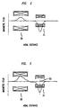
- FIG. 2 illustrates the magnetic flux as a function of distance along the optical axis relative to the position of magnetic lenses 30 and 31. In the region between lenses 30 and 31 the magnetic flux is zero. This is the desired field-free space.
- the mutual focal plane of lenses 30 and 31 is at the apertured scatter filter 19.
- the electron beam scans about the optical axis.
- the bore of the doublet lens is increased while the axial separation between the two lenses either remains the same or is shortened to control space-charge blur. Consequently, the magnetic fields of the doublet lens overlap. This problem is illustrated in FIG. 3.
- the magnetic flux of each lens is affected by this overlap. This is observed with reference to dashed line 50 in FIG. 3. Observe that, due to the proximity between lenses 30 and 31, the flux as a function of axial position for lens 31 on one side of line 50 is not a mirror image of flux as a function of axial position on the other side of line 50. Thus, the desired axial magnetic field symmetry for lens 31 (and for lens 30) in FIG. 3 is not preserved.
- This overlap causes field distortion. Also, the apertured scatter filter 19 is immersed in the magnetic field of lenses 30 and 31. Since this field overlap compounds aberrations and total blur growth and also causes projection magnification changes. Consequently, a solution to the magnetic field overlap of the projection lens doublet that is compatible with the SCALPEL® tool design is sought.
- the present invention is directed to a magnetic doublet lens system in which the spacing between the two lenses is such that their magnetic fields overlap.
- the magnetic doublet lens system is equipped with magnetic clamps that effect substantial separation of the magnetic fields.
- the magnetic clamps are made of a ferromagnetic material.
- the present invention is also directed to an apparatus for electron beam lithography that has a magnetic doublet lens system that is equipped with magnetic clamps to effect substantial separation of the magnetic fields between the two lenses.
- Substantial separation in the context of the present invention, is sufficient separation of ensure that the magnetic field of one lens in the doublet lens system is not adversely affected by the magnetic field of the other lens in the magnetic doublet lens system.
- Adverse affects are doublet compound image aberrations, total blur growth and projection magnification changes attributable to magnetic field overlap.
- the magnetic clamps have a configuration and placement that preserves the symmetry of the magnetic doublet lens and the common focal plane of the two lenses in the magnetic doublet lens system.
- the magnetic doublet lens is designed for 4:1 image demagnification (i.e., image reduction)
- the magnetic clamps are designed to preserve this relationship.
- An example of a suitable clamp design for such a magnetic doublet lens is one in which the dimensional relationship (i.e. for cylindrical clamps the ratio of height and diameter) is also 4:1.
- magnetic clamps are inserted between the individual lenses in a magnetic doublet lens system.
- an apertured scatter filter is inserted in an essentially field-free space between the two lenses, wherein the essentially field-free space is provided by the magnetic clamps.
- the essentially field-free space is obtained by using the magnetic clamps to effect substantial separation of the magnetic fields of the two lenses.
- substantially separating the magnetic fields doublet compound aberrations, total blur growth and projection magnification changes attributable to magnetic field overlap are avoided.
- magnetic lenses have a spherical aberration co-efficient (C sph ) that is proportional to the integral of the magnetic field flux density first derivative squared (dB/dz) 2 dz. This is characterized by the following formula: C sph ⁇ (dB/dz) 2 dz.
- C sph spherical aberration co-efficient
- Other aberrations and distortions depend on the field distribution B(z) in the same way. Any distortion in the magnetic field is likely to add aberrations and distortions into the final image.
- magnetic clamps are designed to prevent distortions in the magnetic field that are caused by overlap of the magnetic fields in the magnetic doublet lens system.
- the magnetic clamps are also designed and placed to preserve the symmetry of the magnetic doublet lens. As one skilled in the art is aware, symmetry is required to maintain beam rotation and related anisotropic aberrations within the limits required for acceptable imaging.
- FIG. 4 illustrates a cross-section of a magnetic lens doublet system 100.
- the magnetic lens doublet system has a first lens 110 and a second lens 120.
- Lens 110 is equipped with magnetic clamp 111.
- Lens 120 is equipped with magnetic clamp 121.
- Magnetic clamps 111 and 121 are a ferromagnetic material, such as soft iron or ferrite. The size, configuration and location of the magnetic clamps are determined by a number of factors. The first factor is that the magnetic clamps prevent the fields from lenses 110 and 120 from substantially penetrating into the region 125 between the magnetic clamps.
- the apertured scatter filter 130 is placed in region 125.
- the second factor is that the magnetic clamps must be configured so as not to interfere with the radiation transmitted through the lens system.
- the third factor is that the magnetic clamps must be sized to preserve the symmetry of the doublet. That relationship is reflected by symmetry of the doublet about the common focal plane of the lens. As previously noted, the desired symmetry of the axial magnetic field of a lens is not preserved when the magnetic fields of the two lenses in the magnetic doublet lens system overlap. Also, if the magnetic doublet lens system provides for a 4:1 image reduction, the magnetic lenses must have a size and a placement along the lens system focal length that preserves that relationship.
- each lens, 210 and 220 of magnetic doublet lens 200 has two magnetic clamps.
- Lens 210 is equipped with lenses 211 and 212.
- Lens 220 is equipped with clamps 221 and 222.
- an apertured scatter filter 230 is placed in the field-free space 225 between lens 210 and lens 220.
- the doublet of the projection lens system of the present invention is described with reference to FIG. 6.
- the lens 310 of doublet lens 300 generates a field 315 (drawn as a series of lines).
- the field 315 is contained by magnetic clamp 311.
- the lens 320 of doublet lens 300 generates a field 325 (drawn as a series of lines).
- the field 325 is contained by magnetic clamp 321.
- the magnetic field lines 315 and 325 do not extend into the space 330 that contains the apertured scatter filter 335.
- Lens 310 is connected to magnetic clamp 311 via connector 339.
- Lens 320 is connected to magnetic clamp 321 via connector 340.
- Connectors 339 and 340 are a magnetic material such as ferrite or soft iron.
- FIG. 7 is a schematic of a magnetic doublet lens system placed in an electron beam lithography tool.
- the tool 400 has an optical axis 405.
- the magnetic doublet lens system 410 is placed between the mask plane 411 and the image plane 412.
- the magnetic doublet lens system 410 has a first lens 415 and a second lens 420. Both lenses 415 and 420 have wound cores and soft iron bodies.
- First lens 415 is coupled to a first magnetic clamp 416.
- Second lens 420 is coupled to a second magnetic clamp 421.
- the clamps are the same material as the body of the lens (soft iron).
- An apertured scatter filter 425 is placed between the first magnetic clamp 416 and the second magnetic clamp 421.
- the lens system 410 is configured to demagnify an image of the mask 411.
- the degree of demagnification is 0.25 (i.e., an image reduction of 4:1).
- the demagnified image is transmitted into an energy sensitive material on a wafer in image plane 412.
- the distance between the mask plane 411 and the apertured scatter filter is 320mm.
- the distance between the image plane 412 and the apertured scatter filter 425 is 80mm.
- the lens system 410 is centered about the optical axis 405. Using the position of the apertured scatter filter 425 on the optical axis 405 as the zero reference point, the focal length of the first lens is -160 mm. The focal length of the second lens is 40 mm. The focal length of lens 415 is illustrated by the distance from the point Z 1A to the apertured scatter filter 425 along the optical axis 405. The focal length of lens 420 is illustrated by the distance from the point Z 1B to the apertured scatter filter 425 along the optical axis 405.
- Lens 415 defines an opening D A that is 120 mm.
- the internal length G A of lens 415 is also 120 mm.
- Lens 420 defines an opening D B that is 30 mm.
- the internal length G B of lens 420 is also 30 mm.
- First magnetic clamp 416 defines an opening D CA that is 40 mm.
- the first magnetic clamp 416 is a distance S CA (80 mm) in a direction parallel to the optical axis.
- Second magnetic clamp 421 defines an opening D CB that is 10 mm.
- the second magnetic clamp 421 is a distance S CB (20 mm) from lens 420 in a direction parallel to the optical axis.
- the performance of the above described lens system was modeled.
- the performance of a system without the first and second magnetic clamps 416 and 421 (but otherwise identical) was also modeled.
- the performance of the two systems was then compared.
- the modeling was performed using second-order finite element modeling software from Munro's Electron Beam Software Ltd. of London, England.
- the comparison provided in Table 1 demonstrates the benefits of magnetic clamps. Specifically, the system without clamps had a much lower rotation angle in the region in which the apertured scatter filter was located compared to the system without clamps. This demonstrates that the field effects in the apertured scatter filter region were much lower in the system without clamps compared to the system with clamps. Furthermore, this improvement was obtained without an adverse effect on magnification, landing angle or beam blur. Also, as demonstrated by the reduction in lens excitation for the lens system with clamps, the lens system of the present invention is more efficient than a lens system without such clamps.
Landscapes
- Engineering & Computer Science (AREA)
- Chemical & Material Sciences (AREA)
- Nanotechnology (AREA)
- Physics & Mathematics (AREA)
- Analytical Chemistry (AREA)
- Crystallography & Structural Chemistry (AREA)
- Condensed Matter Physics & Semiconductors (AREA)
- General Physics & Mathematics (AREA)
- Manufacturing & Machinery (AREA)
- Electromagnetism (AREA)
- Mathematical Physics (AREA)
- Theoretical Computer Science (AREA)
- Electron Beam Exposure (AREA)
Abstract
Description
| Without Clamps | With Clamps | |
| Lens Excitation (AT) | 2112.71 | 2103.06 |
| Magnification | 0.2509 | 0.2501 |
| Rotation Angle (mrad) | -0.946 | -0.0262 |
| Landing Angle (mrad) | 0.12 | 0.12 |
| Beam Blur at center (nm) | 19.3 | 19.3 |
| Beam Blur at corner (nm) | 33.0 | 32.6 |
Claims (6)
- An apparatus for projection lithography comprising:a lens system comprising at least one magnetic doublet lens and a back focal plane filter positioned in the back focal plane or some equivalent conjugate plane of the magnetic doublet lens in the lens system, the back focal plane filter having a first aperture which is adapted to transmit insignificantly scattered radiation from a radiation source therethrough wherein the magnetic doublet lens system has a pair of ferromagnetic clamps, a first clamp associated with the first lens in the magnetic doublet lens system and a second clamp associated with the second lens in the magnetic lens, wherein the first clamp and the second clamp are configured to substantially separate the magnetic field of the first lens from the magnetic field of the second lens.
- The apparatus of claim 1 wherein the magnetic clamps are made of a magnetic material.
- The apparatus of claim 1 wherein the back focal plane filter is placed between the two lenses of the magnetic doublet lens and wherein the clamps are placed and configured to prevent the magnetic fields of the first and second lens from extending to the back focal plane filter.
- The apparatus of claim 2 wherein the magnetic material is a ferromagnetic material.
- The apparatus of claim 1 wherein the magnetic doublet lens has a symmetry for image magnification or demagnification and wherein the first and second clamps have a geometry and dimensions that are selected to preserve the symmetry of the magnetic doublet lens.
- The apparatus of claim 5 wherein the magnetic doublet lens provides 4:1 image demagnification and the first clamp and the second clamp have a dimensional relationship such that the dimensions of the first clamp are four times the dimensions of the second clamp.
Applications Claiming Priority (2)
| Application Number | Priority Date | Filing Date | Title |
|---|---|---|---|
| US15826899P | 1999-10-07 | 1999-10-07 | |
| US158268P | 1999-10-07 |
Publications (2)
| Publication Number | Publication Date |
|---|---|
| EP1091383A2 true EP1091383A2 (en) | 2001-04-11 |
| EP1091383A3 EP1091383A3 (en) | 2005-01-19 |
Family
ID=22567355
Family Applications (1)
| Application Number | Title | Priority Date | Filing Date |
|---|---|---|---|
| EP00302982A Withdrawn EP1091383A3 (en) | 1999-10-07 | 2000-04-07 | Electron beam imaging apparatus |
Country Status (4)
| Country | Link |
|---|---|
| US (1) | US6420714B1 (en) |
| EP (1) | EP1091383A3 (en) |
| JP (1) | JP2001160536A (en) |
| KR (1) | KR100418231B1 (en) |
Families Citing this family (2)
| Publication number | Priority date | Publication date | Assignee | Title |
|---|---|---|---|---|
| US8039813B2 (en) * | 2005-09-06 | 2011-10-18 | Carl Zeiss Smt Gmbh | Charged particle-optical systems, methods and components |
| TWI477925B (en) | 2011-10-04 | 2015-03-21 | 紐富來科技股份有限公司 | Multi - beam charged particle beam mapping device and multi - beam charged particle beam rendering method |
Family Cites Families (15)
| Publication number | Priority date | Publication date | Assignee | Title |
|---|---|---|---|---|
| JPS5463681A (en) | 1977-10-29 | 1979-05-22 | Nippon Aviotronics Kk | Electron beam exposure device |
| US4929838A (en) * | 1988-02-16 | 1990-05-29 | Fujitsu Limited | Magnetic object lens for an electron beam exposure apparatus which processes a wafer carried on a continuously moving stage |
| US5172473A (en) | 1990-05-07 | 1992-12-22 | International Business Machines Corporation | Method of making cone electrical contact |
| US5260151A (en) * | 1991-12-30 | 1993-11-09 | At&T Bell Laboratories | Device manufacture involving step-and-scan delineation |
| US5624774A (en) * | 1994-06-16 | 1997-04-29 | Nikon Corporation | Method for transferring patterns with charged particle beam |
| US5633507A (en) | 1995-09-19 | 1997-05-27 | International Business Machines Corporation | Electron beam lithography system with low brightness |
| JPH09180987A (en) | 1995-12-26 | 1997-07-11 | Nikon Corp | Charged particle beam transfer device |
| JPH09223475A (en) | 1996-02-19 | 1997-08-26 | Nikon Corp | Electromagnetic deflector and charged particle beam transfer apparatus using the deflector |
| JP3927620B2 (en) | 1996-06-12 | 2007-06-13 | キヤノン株式会社 | Electron beam exposure method and device manufacturing method using the same |
| JPH10142397A (en) * | 1996-11-07 | 1998-05-29 | Nikon Corp | Electron optics |
| JPH10302691A (en) * | 1997-04-23 | 1998-11-13 | Nikon Corp | Projection lens system |
| JPH10302696A (en) * | 1997-04-23 | 1998-11-13 | Nikon Corp | Electron beam projection lens |
| US6064071A (en) * | 1997-04-23 | 2000-05-16 | Nikon Corporation | Charged-particle-beam optical systems |
| JPH1154412A (en) * | 1997-07-30 | 1999-02-26 | Nikon Corp | Electron beam reduction transfer device |
| JPH11265672A (en) * | 1998-03-16 | 1999-09-28 | Nikon Corp | Optical system for charged beam device |
-
2000
- 2000-04-07 EP EP00302982A patent/EP1091383A3/en not_active Withdrawn
- 2000-06-09 US US09/591,626 patent/US6420714B1/en not_active Expired - Lifetime
- 2000-10-06 JP JP2000306942A patent/JP2001160536A/en active Pending
- 2000-10-06 KR KR10-2000-0058700A patent/KR100418231B1/en not_active Expired - Fee Related
Also Published As
| Publication number | Publication date |
|---|---|
| JP2001160536A (en) | 2001-06-12 |
| EP1091383A3 (en) | 2005-01-19 |
| KR20010050883A (en) | 2001-06-25 |
| KR100418231B1 (en) | 2004-02-11 |
| US6420714B1 (en) | 2002-07-16 |
Similar Documents
| Publication | Publication Date | Title |
|---|---|---|
| TW559883B (en) | Charged particle beam exposure apparatus, device manufacturing method, and charged particle beam applied apparatus | |
| US5831270A (en) | Magnetic deflectors and charged-particle-beam lithography systems incorporating same | |
| WO2000075281A2 (en) | Supercritical fluid-assisted nebulization and bubble drying | |
| US6180947B1 (en) | Multi-element deflection aberration correction for electron beam lithography | |
| JP2001077018A (en) | Lithographic printing method for forming an exposed pattern on a substrate | |
| JPH0536585A (en) | Image projection method and semiconductor device manufacturing method using the method | |
| EP1610358A1 (en) | Aberration correction device and method for operating same | |
| US6777166B2 (en) | Particle-optical lens arrangement and method employing such a lens arrangement | |
| US5801388A (en) | Particle beam, in particular ionic optic imaging system | |
| US6420714B1 (en) | Electron beam imaging apparatus | |
| US6455863B1 (en) | Apparatus and method for forming a charged particle beam of arbitrary shape | |
| US6452193B1 (en) | Electron beam exposure apparatus, electron lens, and device manufacturing method | |
| KR100577754B1 (en) | Apparatus and Method for Electron Beam Lithography | |
| JP4468753B2 (en) | Charged particle beam exposure apparatus and device manufacturing method using the apparatus | |
| US6831260B2 (en) | Electron beam exposure apparatus, reduction projection system, and device manufacturing method | |
| JPH11297610A (en) | Charged particle beam exposure system | |
| JP2001007021A (en) | Charged particle beam projection lithography with variable beam shape | |
| EP1046185B1 (en) | Projection lithography device utilizing charged particles | |
| EP1091384A2 (en) | Electron beam imaging apparatus | |
| WO2000014767A1 (en) | Quadrupole device for projection lithography by means of charged particles | |
| JP2000164501A (en) | Charged particle beam exposure system | |
| JPH10302696A (en) | Electron beam projection lens | |
| JPH05226209A (en) | Ion optical drawing device | |
| JP2003124097A (en) | Mask, method of manufacturing the same, exposure apparatus, and method of manufacturing a semiconductor device | |
| JP2001168025A (en) | Electron beam imaging device |
Legal Events
| Date | Code | Title | Description |
|---|---|---|---|
| PUAI | Public reference made under article 153(3) epc to a published international application that has entered the european phase |
Free format text: ORIGINAL CODE: 0009012 |
|
| AK | Designated contracting states |
Kind code of ref document: A2 Designated state(s): AT BE CH CY DE DK ES FI FR GB GR IE IT LI LU MC NL PT SE |
|
| AX | Request for extension of the european patent |
Free format text: AL;LT;LV;MK;RO;SI |
|
| PUAL | Search report despatched |
Free format text: ORIGINAL CODE: 0009013 |
|
| AK | Designated contracting states |
Kind code of ref document: A3 Designated state(s): AT BE CH CY DE DK ES FI FR GB GR IE IT LI LU MC NL PT SE |
|
| AX | Request for extension of the european patent |
Extension state: AL LT LV MK RO SI |
|
| RIC1 | Information provided on ipc code assigned before grant |
Ipc: 7H 01J 37/153 B Ipc: 7H 01J 37/30 B Ipc: 7H 01J 37/317 B Ipc: 7H 01J 37/141 A |
|
| AKX | Designation fees paid | ||
| STAA | Information on the status of an ep patent application or granted ep patent |
Free format text: STATUS: THE APPLICATION IS DEEMED TO BE WITHDRAWN |
|
| 18D | Application deemed to be withdrawn |
Effective date: 20050720 |
|
| REG | Reference to a national code |
Ref country code: DE Ref legal event code: 8566 |