EP1089593A2 - Ceramic heater - Google Patents
Ceramic heater Download PDFInfo
- Publication number
- EP1089593A2 EP1089593A2 EP00308583A EP00308583A EP1089593A2 EP 1089593 A2 EP1089593 A2 EP 1089593A2 EP 00308583 A EP00308583 A EP 00308583A EP 00308583 A EP00308583 A EP 00308583A EP 1089593 A2 EP1089593 A2 EP 1089593A2
- Authority
- EP
- European Patent Office
- Prior art keywords
- plural
- ceramic heater
- portions
- ceramic substrate
- current
- Prior art date
- Legal status (The legal status is an assumption and is not a legal conclusion. Google has not performed a legal analysis and makes no representation as to the accuracy of the status listed.)
- Withdrawn
Links
Images


Classifications
-
- H—ELECTRICITY
- H05—ELECTRIC TECHNIQUES NOT OTHERWISE PROVIDED FOR
- H05B—ELECTRIC HEATING; ELECTRIC LIGHT SOURCES NOT OTHERWISE PROVIDED FOR; CIRCUIT ARRANGEMENTS FOR ELECTRIC LIGHT SOURCES, IN GENERAL
- H05B3/00—Ohmic-resistance heating
- H05B3/10—Heating elements characterised by the composition or nature of the materials or by the arrangement of the conductor
-
- H—ELECTRICITY
- H05—ELECTRIC TECHNIQUES NOT OTHERWISE PROVIDED FOR
- H05B—ELECTRIC HEATING; ELECTRIC LIGHT SOURCES NOT OTHERWISE PROVIDED FOR; CIRCUIT ARRANGEMENTS FOR ELECTRIC LIGHT SOURCES, IN GENERAL
- H05B3/00—Ohmic-resistance heating
- H05B3/10—Heating elements characterised by the composition or nature of the materials or by the arrangement of the conductor
- H05B3/12—Heating elements characterised by the composition or nature of the materials or by the arrangement of the conductor characterised by the composition or nature of the conductive material
- H05B3/14—Heating elements characterised by the composition or nature of the materials or by the arrangement of the conductor characterised by the composition or nature of the conductive material the material being non-metallic
- H05B3/141—Conductive ceramics, e.g. metal oxides, metal carbides, barium titanate, ferrites, zirconia, vitrous compounds
- H05B3/143—Conductive ceramics, e.g. metal oxides, metal carbides, barium titanate, ferrites, zirconia, vitrous compounds applied to semiconductors, e.g. wafers heating
-
- H—ELECTRICITY
- H05—ELECTRIC TECHNIQUES NOT OTHERWISE PROVIDED FOR
- H05B—ELECTRIC HEATING; ELECTRIC LIGHT SOURCES NOT OTHERWISE PROVIDED FOR; CIRCUIT ARRANGEMENTS FOR ELECTRIC LIGHT SOURCES, IN GENERAL
- H05B3/00—Ohmic-resistance heating
- H05B3/20—Heating elements having extended surface area substantially in a two-dimensional [2D] plane, e.g. plate-heater
- H05B3/22—Heating elements having extended surface area substantially in a two-dimensional [2D] plane, e.g. plate-heater non-flexible
- H05B3/28—Heating elements having extended surface area substantially in a two-dimensional [2D] plane, e.g. plate-heater non-flexible heating conductor embedded in insulating material
- H05B3/283—Heating elements having extended surface area substantially in a two-dimensional [2D] plane, e.g. plate-heater non-flexible heating conductor embedded in insulating material the insulating material being an inorganic material, e.g. ceramic
Definitions
- the present invention relates to ceramic heater, more particularly ceramic heaters to be favorably used in semiconductor-producing apparatuses such as semiconductor-producing apparatuses and etching apparatuses.
- the semiconductor-producing apparatus is provided with a ceramic heat generator for heating wafers as substrates.
- inner and outer resistance heat generators made of a high melting point metal are buried in the ceramic substrate, and separate current-introducing terminals are provided for the respective resistance heat generators.
- the inner resistance heat generator and the outer resistance heat generator are independently controlled by independently applying voltages to them, respectively.
- such a ceramic heater employs a so called two-zone heater structure.
- JP-A 5-326,112 describes that a heat generator of a ceramic heater is constituted by plural circuit patterns made of a high melting point metal, and these circuit patterns are so arranged to compensate defect portions with respect to each other or one another. More specifically, this is realized by overlapping a bent or return portion of one circuit pattern with another circuit pattern.
- the ceramic substrate and the resistance heat generators are extremely frequently heated and cooled.
- a difference in coefficient of thermal expansion between the ceramic substrate and the high melting point metal constituting the resistance heat generators causes shearing stress in the current-introducing terminals connected to the resistance heat generators.
- the resistance heat generator is generally bonded to the current-introducing terminal with a brazing material, such bonded portions are sometimes broken by shearing stress due to difference in thermal expansion between the resistance heat generator and the brazing material.
- the ceramic heater according to the present invention comprises a ceramic substrate having a heating face, and a resistance heat generator buried in the ceramic substrate, wherein the resistance heat generator comprises plural planar resistance heating elements arranged in a layered fashion as viewed in a thickness direction of the ceramic substrate, and each of said plural planar heating elements comprises a heat generation density-increased portion, and the heat generation density-increased portions of the respective plural planar heating elements are located in different portions, respectively.
- the heat generation density-increased portions of the respective planar heating elements may be partially overlapping located in different portions, respectively. Therefore, the feature "the heat generation density-increased portions of the respective planar heating elements are located in different portions, respectively" encompasses this overlapped manner.
- the respective portions of relatively higher heat energy output rate (heat generation density-increased portions) of the different heating elements may be laterally offset from each other, either with or without partial overlap, as seen looking in plan view on a major face of the heater.
- the portion or portions of higher heat energy output rate is adjacent a portion or portions of relatively lower heat energy output rate.
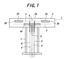
- Fig. 1 is a sectional view of an embodiment of the ceramic heater according to the present invention.
- Fig. 2 is a sectional view of another embodiment of the ceramic heater according to the present invention.
- Fig. 3 is a figure for illustrating a producing process as an example to produce a ceramic heater according to the present invention.
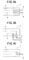
- Figs. 4(a) to 4(c) illustrate cases where the current-introducing terminal portions 5 and 6 are connected to the outer peripheral portions of the planar resistance heating elements 3 and 4, respectively, substantially in parallel to the planar resistance heating elements through the terminals.
- Fig. 1 is a sectional view of an embodiment of the ceramic heater according to the present invention. In each figure, details are omitted and parts are drawn in different scales for the purpose of clarified explanation.
- the ceramic heater 1 As shown in Fig. 1, the ceramic heater 1 according to the present invention comprises a ceramic substrate 2, and an upper planar resistance heating element 3 and a lower planar resistance heating element 4 arranged in a layered fashion as viewed in a thickness direction of the ceramic heater.
- Current-introducing terminal portions 5 and 6 are provided in a central portion of the ceramic substrate 2.
- the upper planar resistance heating element 3 and the lower planar resistance heating element 4 are arranged substantially in parallel to a heating face 2A of the ceramic substrate 2.
- the upper planar resistance heating element 3 has a heat generation density-increased portion 3A at an outer peripheral portion
- the lower planar resistance heating element 4 has a heat generation density-increased portion 4A at an inner peripheral portion.
- One end of the current-introducing terminal portion 5 is connected to the upper planar resistance heating element 3, and one end of the current-introducing terminal portion 6 is connected to the heat generation density-increased portion 4A of the lower planar resistance heating element 4.
- the other end of each of the current-introducing terminal portions 5 and 6 is connected to lead wires 8 or 9, respectively.
- the ceramic substrate 2 is provided with a cylindrical hollow portion 7 at its under portion, which protects the other ends of the current-introducing terminal portions 5 and 6, i.e., those portions of the terminal portions which come out of the ceramic substrate 2.
- the entire ceramic substrate 2 can be relatively uniformly heated. Consequently, occurrence of cracking owing to temperature variations in the ceramic substrate 2 can be prevented.
- JP-A 5-326,112 describes the invention in which a plurality of the circuit patterns are merely arranged to compensate their defect portions.
- the "heat generation density-increased portions" are provided for the plural planar resistance heating elements, corresponding to the plural circuit patterns in JP-A 5-326,112, at different locations.
- heat generation density-increased portions can compensate the defect portions of the planar resistance heating elements as in the same way as JP-A 5-326,112. This compensation is made exclusively by the heat generation density-increased portion, not by the arrangement of the circuit patterns. Further, the heat generation density-increased portion is a completely different concept from that of the arrangement of the plural circuit patterns to mutually compensate their defect portions.
- the ceramic heater according to the present invention needs to be provided with a plurality of planar resistance heating elements in a layered fashion as viewed in a thickness direction of the ceramic substrate.
- the ceramic heater 1 shown in Fig. 1 comprises two, i.e., an upper planar resistance heating element 3 and a lower planar resistance heating element 4.
- the number of the planar resistance heating elements is not particularly limited, so long as the above requirements are met.
- the object of the present invention can be sufficiently accomplished by providing two or three planar resistance heating elements.
- the plural planar resistance heating elements of the ceramic heater according to the present invention need to include their heat generation density-increased portions located in different positions.
- the plural planar resistance heating elements include their heat generation density-increased portions like this and for example if the upper planar resistance heating element 3 shown in Fig. 1 does not generate heat, the ceramic substrate 2, and in turn a target object on the heating face 2A can be uniformly heated with much heat from the heat generation density-increased portion of the lower planar resistance heating element 4.
- the heat generation density-increased portions are provided for the planar resistance heating elements at different positions and when at least two of the plural planar resistance heating elements generate heat, the amount of heat generated from each of the heat generation density-increased portions becomes uniform within the ceramic substrate. Therefore, cracking can be prevented within the ceramic substrate, and the target object can be uniformly heated.
- the upper planar resistance heating element 3 and the lower resistance heating element 4 are arranged substantially in parallel to the heating face 2A of the ceramic substrate 2.
- variations in the temperature distribution within the heating face of the ceramic substrate are preferably within 50°C and more preferably within 20°C between the maximum temperature and the minimum temperature in case that the heating is effected with each of the planar resistance heating element. If such variation in the temperature distribution within the heating face of the ceramic substrate are suppressed to not more than 50°C between the maximum temperature and the minimum temperature in case that heating is effected with each planar resistance heating element, cracking of the ceramic heater can be more effectively prevented. For example, even if no current flows through the upper planar resistance heating element 3 in Fig. 1 to disable functioning of the heating element 3 as a heater, the substrate can be uniformly heated with the lower planar resistance heating element 4 only. Consequently, cracking due to non-uniform temperature distribution within the ceramic substrate can be more effectively suppressed, and the target object on the heating face 2A can be more uniformly heated.
- a current-introducing terminal portion 5 is connected to the upper planar resistance heating element 3 at a position different from the heat generation density-increased portion 3A. Since the current-introducing terminal portion is to be connected to the heat generation density-increased portion, a relatively large amount of a brazing material is required, so that the connecting portion is likely to be broken owing to a difference in thermal expansion between them. Therefore, when the current-introducing terminal portion is connected as mentioned above, a case where all the connections between the planar resistance heating elements and the current-introducing terminal portions are cut can be prevented.
- the current-introducing terminal portion 5 may be connected, for example, to an outer peripheral portion 3B of the upper planar resistance heating element 3 in Fig. 1.
- the current-introducing terminal portions 5 and 6 are arranged to gather in a central portion of the ceramic substrate 2.
- the ceramic heater can be easily placed in a chamber, and the current flowing through a plurality of the resistance heating elements can be controlled with a single thermocouple by appropriately setting the power ratio between them.
- Fig. 2 is a sectional view for illustrating another ceramic heater according to the present invention.
- same or similar reference numbers as in Fig. 1 are used for identical or similar parts.
- a current-introducing terminal portion for an upper planar resistance heating element 3 is constituted by an anode terminal 15A and a cathode terminal 15B.
- a current-introducing terminal portion for an upper planar resistance heating element 4 is constituted by an anode terminal 16A and a cathode terminal 16B.
- the terminals 15A, 15B, 16A and 16B are arranged in respective side portions such that the anode terminals 15A and 16A are united, and the cathode terminals 15B and 16B are united, whereas the former are separated from the latter. This arrangement of the terminals can suppress the occurrence of discharge between the terminals.
- the configuration of the planar resistive heating elements in the ceramic heater according to the present invention is not limited, so long as the object of the present invention can be realized.
- the ceramic heater may be constituted by a network member, a coil member, a ribbon-shaped member or the like.
- the planar resistance heating element is preferably constituted by the network member or the coil member.
- the planar shape of the planar resistance heating element is not particularly limited.
- the heat generation density-increased portion is formed by knitting wires at a higher density at a given location or reducing the sectional area of the wire constituting the network member at a given location.
- the heat generation density-increased portion can be formed by increasing the number of windings or the pitch at a given location or by increasing the diameter of concentric turns of the coil at such a given location.
- the heat generation density-increased portion can be formed by reducing the width of the ribbon at a given location.
- the ceramic substrate in the present invention may be produced from a known ceramic material selected from nitride ceramics such as aluminum nitride, silicon nitride, boron nitride and sialon and known ceramic materials such as an alumina-silicon carbide composite material.
- nitride ceramics such as aluminum nitride, silicon nitride, boron nitride and sialon
- known ceramic materials such as an alumina-silicon carbide composite material.
- aluminum nitride is preferred.
- planar resistance heating element high melting point metals such as tantalum, tungsten, molybdenum, platinum, rhenium, hafnium and alloys thereof may be preferably used. Particularly, if the ceramic substrate is constituted with aluminum nitride, molybdenum or a molybdenum alloy is preferred.
- conductive materials such as carbon, TiN and TiC may be used.
- the ceramic heater shown in Fig. 1 is produced as follows.
- Fig. 3 is a flowchart showing an example of a method for producing the ceramic heater according to the present invention shown in Fig. 1.
- a powdery ceramic material such as aluminum nitride to constitute the ceramic substrate 2 is preliminarily mixed with a binder by a trommel or the like, the resulting mixture is granulated by a spray granulator.
- a first preliminarily molded body 24 is obtained by uniaxial press molding.
- a network-shaped conductive member 3M to constitute the upper planar resistance heating element 3 and first members 5M to constitute the current-introducing terminal portion 5 are placed on the first preliminarily molded body 24, and the granulated material 25 is charged on the conductive member 3M and the first preliminarily molded body 24 so that the surrounding of the first members 5M may be filled with the granulated material.
- the resultant is uniaxially press molded with the mold 21, the lower punch 22 and the upper punch 23, thereby forming a second preliminarily molded body 26.
- a network-shaped conductive member 4M to constitute the lower planar resistance heating element 4 and members 6M to constitute the current-introducing terminal portion 6 are placed on the second preliminarily molded body 26, and second members 5N to constitute the current-introducing terminal portions 5 are placed on the first members 5N, respectively.
- the granulated material 25 is charged on the conductive member 4M and the second preliminarily molded body 26 so that the surrounding of the members 6M and the second members 5N may be filled with the granulated material.
- the resultant is uniaxially press molded with the mold 21, the lower punch 22 and the upper punch 23 in the same manner as above, thereby forming a molded body 27.
- the thus obtained molded body 27 is subjected to an ordinary hot press, thereby obtaining a sintered body.
- the ceramic heater 1 as shown in Fig. 1 or 2 can be finally obtained by attaching the cylindrical hollow portion 7 and the lead wires to the sintered body by mechanical tightening, brazing joint, glass joint, a diffusion joint or the like.
- the molding pressure under which the first molded body is obtained as well as the sintering condition in the hot press are arbitrarily set depending upon the kind and the particle diameter of the ceramic material, the finish dimension, etc.
- the ceramic heater is not limited to the above-mentioned embodiments, but any variations and modifications may be made so long as they fall outside the scope of the claimed invention.
- the heat generation density-increased portion of the upper planar resistance heating element and that of the lower planar resistance heating element may be formed at inner and outer peripheral portions, respectively.
- At least one of the plural current-introducing terminal portions may be connected to the outer periphery of the planar resistance heating element substantially in parallel to the planar resistance heating element.
- Figs. 4(a) to 4(c) illustrate cases where the current-introducing terminal portions 5 and 6 are connected to the outer peripheral portions of the planar resistance heating elements 3 and 4, respectively, substantially in parallel to the planar resistance heating elements through the terminals.
- the ceramic heater of the present invention in which the plural resistance heating elements are arranged to uniformly heat objects to be heated, such as semiconductor wafers, no crack is formed even if a part of the resistance heating elements is broken. Consequently, the ceramic heater which can be stably operated can be offered.
Landscapes
- Chemical & Material Sciences (AREA)
- Engineering & Computer Science (AREA)
- Ceramic Engineering (AREA)
- Inorganic Chemistry (AREA)
- Resistance Heating (AREA)
- Surface Heating Bodies (AREA)
Abstract
Description
Claims (10)
- A ceramic heater comprising a ceramic substrate having a heating face, and a resistance heat generator buried in the ceramic substrate, wherein the resistance heat generator comprises plural planar resistance heating elements arranged in a layered fashion as viewed in a thickness direction of the ceramic substrate, and each of said plural planar heating elements comprises a heat generation density-increased portion, and the heat generation density-increased portions of the respective plural planar heating elements are located in different portions, respectively.
- The ceramic heater set forth in claim 1, wherein the planar resistance heating elements are arranged substantially in parallel to the heating face of the ceramic substrate.
- The ceramic heater set forth in claim 1 or 2, wherein when the ceramic heater is heated with any one of said planar resistance heating elements, variations in a temperature distribution within the heating face of the ceramic substrate are not more than 50°C.
- The ceramic heater set forth in any one of claims 1 to 3, which further comprises plural current-introducing terminal portions and wherein said current introducing terminals are connected to said plural planar resistance heating elements, respectively, and at least one of said plural current-introducing terminal portions is connected to the planar resistance heating element at a portion different from the heat generation density-increased portion.
- The ceramic heater set forth in claim 4, wherein at least one of said plural current-introducing terminal portions is connected to an outer peripheral portion of said plural resistance heat generation elements and substantially in parallel to the planar heat generation element.
- The ceramic heater set forth in claims 4 or 5, wherein said plural current-introducing terminals are arranged in such a manner that they pass through a portion of the ceramic substrate in a collected manner.
- The ceramic heater set forth in claim 6, wherein said ceramic substrate further comprises a cylindrical portion wherein at least a part of said plural current-introducing terminals portions are arranged inside the cylindrical hollow portion.
- The ceramic heater set forth in claim 4 or 5, wherein each of said current-introducing terminal portions comprises an anode terminal and a cathode terminal, the anode terminals of said plurality current-introducing terminal portions are separated from the cathode terminals of said plural current-introducing portions, and each of the anode terminals and the cathode terminals are arranged in such a manner that they pass through a portion of the ceramic substrate.
- The ceramic heater set forth in claim 8, wherein said ceramic substrate further comprises plural cylindrical portions wherein at least a part of said plural anode terminals and at least a part of said plural cathode terminals are arranged inside the cylindrical hollow portions, respectively.
- The ceramic heater set forth in any one of claims 1 to 9, wherein each of the planar resistance heating elements comprises a network member or a coil spring-shaped member.
Applications Claiming Priority (2)
| Application Number | Priority Date | Filing Date | Title |
|---|---|---|---|
| JP28111599A JP2001102157A (en) | 1999-10-01 | 1999-10-01 | Ceramic heater |
| JP28111599 | 1999-10-01 |
Publications (2)
| Publication Number | Publication Date |
|---|---|
| EP1089593A2 true EP1089593A2 (en) | 2001-04-04 |
| EP1089593A3 EP1089593A3 (en) | 2002-08-28 |
Family
ID=17634573
Family Applications (1)
| Application Number | Title | Priority Date | Filing Date |
|---|---|---|---|
| EP00308583A Withdrawn EP1089593A3 (en) | 1999-10-01 | 2000-09-29 | Ceramic heater |
Country Status (4)
| Country | Link |
|---|---|
| EP (1) | EP1089593A3 (en) |
| JP (1) | JP2001102157A (en) |
| KR (1) | KR20010067260A (en) |
| TW (1) | TW483285B (en) |
Cited By (7)
| Publication number | Priority date | Publication date | Assignee | Title |
|---|---|---|---|---|
| US6437299B1 (en) * | 1999-06-29 | 2002-08-20 | Sumitomo Electric Industries, Ltd. | Heating apparatus for splice protector with separate heating conductor patterns |
| WO2004032187A3 (en) * | 2002-09-19 | 2004-07-01 | Applied Materials Inc | Multi-zone resitive heater |
| US7417206B2 (en) | 2004-10-28 | 2008-08-26 | Kyocera Corporation | Heater, wafer heating apparatus and method for manufacturing heater |
| US8481892B2 (en) | 2009-03-30 | 2013-07-09 | Ngk Insulators, Ltd. | Ceramic heater and method for producing same |
| CN112673709A (en) * | 2018-10-11 | 2021-04-16 | 日本发条株式会社 | Stage, film forming apparatus, and film processing apparatus |
| US12127310B2 (en) | 2017-11-21 | 2024-10-22 | Watlow Electric Manufacturing Company | Multi-zone pedestal heater without vias |
| US12635479B2 (en) | 2022-03-29 | 2026-05-19 | Niterra Co., Ltd. | Substrate holder |
Families Citing this family (21)
| Publication number | Priority date | Publication date | Assignee | Title |
|---|---|---|---|---|
| US6423949B1 (en) | 1999-05-19 | 2002-07-23 | Applied Materials, Inc. | Multi-zone resistive heater |
| JP4744016B2 (en) * | 2001-06-29 | 2011-08-10 | 京セラ株式会社 | Manufacturing method of ceramic heater |
| JP3897563B2 (en) | 2001-10-24 | 2007-03-28 | 日本碍子株式会社 | Heating device |
| JP3925702B2 (en) | 2002-03-18 | 2007-06-06 | 日本碍子株式会社 | Ceramic heater |
| JP4026761B2 (en) | 2002-03-28 | 2007-12-26 | 日本碍子株式会社 | Ceramic heater |
| JP2005197074A (en) | 2004-01-07 | 2005-07-21 | Ngk Insulators Ltd | Resistance heating element and heater |
| JP2005285355A (en) | 2004-03-26 | 2005-10-13 | Ngk Insulators Ltd | Heating device |
| JP4640842B2 (en) * | 2006-10-11 | 2011-03-02 | 日本碍子株式会社 | Heating device |
| KR101177749B1 (en) * | 2007-11-27 | 2012-08-29 | 주식회사 코미코 | Ceramic heater, method for manufacturing the same, and apparatus for depositing a thin film having the same |
| US8637794B2 (en) * | 2009-10-21 | 2014-01-28 | Lam Research Corporation | Heating plate with planar heating zones for semiconductor processing |
| US8791392B2 (en) | 2010-10-22 | 2014-07-29 | Lam Research Corporation | Methods of fault detection for multiplexed heater array |
| US9633875B2 (en) * | 2015-03-13 | 2017-04-25 | Varian Semiconductor Equipment Associates, Inc. | Apparatus for improving temperature uniformity of a workpiece |
| JP6567895B2 (en) * | 2015-06-29 | 2019-08-28 | 京セラ株式会社 | Sample holder and sample processing apparatus equipped with the same |
| KR102348108B1 (en) | 2015-10-05 | 2022-01-10 | 주식회사 미코세라믹스 | Substrate heating apparatus with enhanced temperature uniformity characteristic |
| JP6767833B2 (en) * | 2016-09-29 | 2020-10-14 | 日本特殊陶業株式会社 | Heating device |
| KR102773262B1 (en) * | 2018-10-11 | 2025-02-28 | 닛폰 하츠죠 가부시키가이샤 | Stage, film forming device and film processing device |
| KR102608397B1 (en) * | 2018-10-16 | 2023-12-01 | 주식회사 미코세라믹스 | Middle zone independent control ceramic heater |
| KR102437076B1 (en) | 2021-08-30 | 2022-08-29 | 주식회사 미코세라믹스 | Substrate heating apparatus with enhanced temperature uniformity characteristic |
| JP7864548B2 (en) * | 2022-05-20 | 2026-05-25 | 日本特殊陶業株式会社 | Ceramic heater |
| KR102940539B1 (en) | 2022-08-18 | 2026-03-18 | 주식회사 미코세라믹스 | Substrate heating apparatus with supressed crack generation |
| KR102615529B1 (en) * | 2023-09-19 | 2023-12-19 | 주식회사 제스코 | An electrostatic chuck with a two-layer heater pattern |
Family Cites Families (3)
| Publication number | Priority date | Publication date | Assignee | Title |
|---|---|---|---|---|
| JPH05326112A (en) * | 1992-05-21 | 1993-12-10 | Shin Etsu Chem Co Ltd | Layered ceramic heater |
| JPH08274147A (en) * | 1995-03-30 | 1996-10-18 | Kyocera Corp | Wafer holding device |
| JPH08236599A (en) * | 1995-02-28 | 1996-09-13 | Kyocera Corp | Wafer holding device |
-
1999
- 1999-10-01 JP JP28111599A patent/JP2001102157A/en active Pending
-
2000
- 2000-08-29 TW TW089117459A patent/TW483285B/en not_active IP Right Cessation
- 2000-09-29 KR KR1020000057290A patent/KR20010067260A/en not_active Ceased
- 2000-09-29 EP EP00308583A patent/EP1089593A3/en not_active Withdrawn
Cited By (10)
| Publication number | Priority date | Publication date | Assignee | Title |
|---|---|---|---|---|
| US6437299B1 (en) * | 1999-06-29 | 2002-08-20 | Sumitomo Electric Industries, Ltd. | Heating apparatus for splice protector with separate heating conductor patterns |
| US6518551B2 (en) * | 1999-06-29 | 2003-02-11 | Sumitomo Electric Industries, Ltd. | Apparatus and a method for heating a protective member for an optical fiber fusion splicing part |
| WO2004032187A3 (en) * | 2002-09-19 | 2004-07-01 | Applied Materials Inc | Multi-zone resitive heater |
| US7417206B2 (en) | 2004-10-28 | 2008-08-26 | Kyocera Corporation | Heater, wafer heating apparatus and method for manufacturing heater |
| US8481892B2 (en) | 2009-03-30 | 2013-07-09 | Ngk Insulators, Ltd. | Ceramic heater and method for producing same |
| US12127310B2 (en) | 2017-11-21 | 2024-10-22 | Watlow Electric Manufacturing Company | Multi-zone pedestal heater without vias |
| CN112673709A (en) * | 2018-10-11 | 2021-04-16 | 日本发条株式会社 | Stage, film forming apparatus, and film processing apparatus |
| CN112673709B (en) * | 2018-10-11 | 2024-02-02 | 日本发条株式会社 | Stage, film forming device and film processing device |
| US12211710B2 (en) | 2018-10-11 | 2025-01-28 | Nhk Spring Co., Ltd. | Stage, film-forming apparatus, and film-processing apparatus |
| US12635479B2 (en) | 2022-03-29 | 2026-05-19 | Niterra Co., Ltd. | Substrate holder |
Also Published As
| Publication number | Publication date |
|---|---|
| EP1089593A3 (en) | 2002-08-28 |
| TW483285B (en) | 2002-04-11 |
| JP2001102157A (en) | 2001-04-13 |
| KR20010067260A (en) | 2001-07-12 |
Similar Documents
| Publication | Publication Date | Title |
|---|---|---|
| JP2001102157A (en) | Ceramic heater | |
| US7189946B2 (en) | Substrate heating device | |
| US7279661B2 (en) | Heating apparatus | |
| KR100407052B1 (en) | Heating apparatus | |
| US7173219B2 (en) | Ceramic heaters | |
| US5683606A (en) | Ceramic heaters and heating devices using such ceramic heaters | |
| US7126092B2 (en) | Heater for wafer processing and methods of operating and manufacturing the same | |
| US6204489B1 (en) | Electrically heated substrate with multiple ceramic parts each having different volume restivities | |
| US7053339B2 (en) | Ceramic heater | |
| US6160244A (en) | Susceptors | |
| US8536496B2 (en) | Adaptable layered heater system | |
| KR100708568B1 (en) | Substrate heating apparatus | |
| US20040206747A1 (en) | Ceramic heater for semiconductor manufacturing/inspecting apparatus | |
| JPH11354260A (en) | Multi-layer ceramic heater | |
| US20040112888A1 (en) | Ceramics heater | |
| JP4640842B2 (en) | Heating device | |
| JP4931376B2 (en) | Substrate heating device | |
| KR20080037879A (en) | Heater and manufacturing method thereof | |
| US7332694B2 (en) | Heating resistances and heaters | |
| US20180096868A1 (en) | Ceramic heater | |
| JPH11176559A (en) | Multi-layer ceramic heater | |
| KR20040035281A (en) | Molding heater for heating semiconductor substrate | |
| JP7636234B2 (en) | Ceramic heater and method for manufacturing ceramic heater | |
| JP2024119674A (en) | Ceramic heater and its manufacturing method | |
| JPH11297626A (en) | Solid device manufacturing equipment |
Legal Events
| Date | Code | Title | Description |
|---|---|---|---|
| PUAI | Public reference made under article 153(3) epc to a published international application that has entered the european phase |
Free format text: ORIGINAL CODE: 0009012 |
|
| AK | Designated contracting states |
Kind code of ref document: A2 Designated state(s): AT BE CH CY DE DK ES FI FR GB GR IE IT LI LU MC NL PT SE |
|
| AX | Request for extension of the european patent |
Free format text: AL;LT;LV;MK;RO;SI |
|
| PUAL | Search report despatched |
Free format text: ORIGINAL CODE: 0009013 |
|
| AK | Designated contracting states |
Kind code of ref document: A3 Designated state(s): AT BE CH CY DE DK ES FI FR GB GR IE IT LI LU MC NL PT SE |
|
| AX | Request for extension of the european patent |
Free format text: AL;LT;LV;MK;RO;SI |
|
| RIC1 | Information provided on ipc code assigned before grant |
Free format text: 7H 05B 3/14 A, 7H 05B 3/28 B, 7H 01L 21/00 B, 7H 01L 21/68 B |
|
| AKX | Designation fees paid |
Designated state(s): DE FR GB |
|
| STAA | Information on the status of an ep patent application or granted ep patent |
Free format text: STATUS: THE APPLICATION IS DEEMED TO BE WITHDRAWN |
|
| 18D | Application deemed to be withdrawn |
Effective date: 20030301 |