EP1089430A2 - A dB-linear variable gain amplifier - Google Patents
A dB-linear variable gain amplifier Download PDFInfo
- Publication number
- EP1089430A2 EP1089430A2 EP00115467A EP00115467A EP1089430A2 EP 1089430 A2 EP1089430 A2 EP 1089430A2 EP 00115467 A EP00115467 A EP 00115467A EP 00115467 A EP00115467 A EP 00115467A EP 1089430 A2 EP1089430 A2 EP 1089430A2
- Authority
- EP
- European Patent Office
- Prior art keywords
- linear
- current
- amplifier
- signal
- response
- Prior art date
- Legal status (The legal status is an assumption and is not a legal conclusion. Google has not performed a legal analysis and makes no representation as to the accuracy of the status listed.)
- Withdrawn
Links
Images


Classifications
-
- H—ELECTRICITY
- H03—ELECTRONIC CIRCUITRY
- H03G—CONTROL OF AMPLIFICATION
- H03G7/00—Volume compression or expansion in amplifiers
Definitions
- the invention relates to a dB-linear variable gain amplifier, and particularly to a temperature compensated dB-linear variable gain amplifier.
- Signals with a wide range of amplitudes such as with audio amplification, often require amplifiers with a log-linear or compression-type response.
- high quality audio may have a range of 64,000 to 1 or greater; representing 1 millivolt to 64 volts. Both values are outside the usable range of many amplifiers, since 1 millivolt will often be too noisy, and 64 volts is too much voltage.
- a compression amplifier for the same range, would have a much smaller and therefore more manageable set of operating voltages.
- compression type amplifiers have a gain that varies with amplitude, and the output may contain substantial distortion products. Many applications are adversely affected by this distortion, which can be shown to be due to large amounts of harmonics introduced in the process of compressing the signal.
- a dB-linear amplifier can achieve substantially the same result with much less harmonics by varying the gain as a function of an externally introduced control signal.
- forming a dB-linear amplifier requires that the compression products be separated from the linear signal being amplified. Attempts to solve this problem have been made many times.
- dB-linear amplifiers are realized with piecewise-linear approximation techniques. The output of the amplifier is controlled by, for example, feed back that varies with operating point. As the control voltage increases the amplifier gain decreases with an approximate fit to a log-linear curve, e. g., an exponential or square law curve.
- All semiconductors are temperature sensitive.
- a technique commonly used in band gap regulators and similar circuits allows the temperature sensitivity to be adjusted, but for the prior art dB-linear amplifiers, the adjustment is performed in a separate step or module, which can lead to multiplying errors between the modules.
- One approach is to make a temperature stable separate amplifier and apply it to a piece-wise linear amplifier. This further increases the cost and complexity of the amplifier.
- a current is introduced through a resistor in series with a diode forward voltage, or Vt, and in parallel with a diode characteristic Vf. That is, the voltage drop across the resistor controls the change in the diode forward drop Vf from Vt to some relatively large forward voltage. The resulting current is exponential, as desired.
- the diode being controlled is part of a transistor to reduce loading effects on the resistor based control circuit.
- bias current points also called idling current
- the bias current points also called idling current
- Fig. 1A 150 shows a typical input current 153 of the type used in the prior art and in the invention as an input to an amplifier.
- Output current 155 illustrates the response of a typical compression amplifier of the prior art to the input current 153.
- Output current 157 illustrates the response of a dB-linear variable gain amplifier of the invention, showing how the dB-linear variable gain amplifier of the invention provides a linear response to the input at a dB-linear variable gain. It will be apparent that distortion products generated by the compression amplifier, which must be tolerated or removed by subsequent processing of the signal, are reduced or eliminated by the dB-linear variable gain amplifier.
- Fig. 2 200 we define the base to base voltage of Q7 203 and Q10 205 as Vx.
- Vt has a known value, as discussed in classical theory, of about 25.9 millivolts at 300°K (degrees Kelvin). It is sometimes called the "thermal" voltage.
- Io/Ii 1/(1+e Vx/Vt ) and Io goes from Ii to 0. This is a common method for implementing VGAs known as current sharing.
- dB-linear VGA The purpose of a dB-linear VGA is to synthesize or approximate Vx to a function such that (2) can be expressed as (1).
- the approach used in this disclosure is an exact synthesis of the function rather than a piece-wise linear approximation.
- the emitter area of Q4 309 is equal to the emitter area of Q9 307, and the emitter area of Q5 303 is equal to the emitter area of Q22 305.
- This block allows a current I2-Ix to be developed as shown. This configuration will be modified to provide temperature stability and to define the desired final result; but Fig 3 conceptually describes the desired relationship for the currents involved.
- a resistor R5 409 has been added.
- Ii 403 an input current, is applied to the base of transistor 407 and to the collector of transistor 405, which are in a feed back configuration.
- a constant current, Ic 411 sets a bias point for the configuration.
- Q8 405 requires more base current to conduct the increased collector current away from the base of Q0 407, so the voltage across R5 409 increases as Q0 407 provides extra base current to Q8 405.
- the base voltage of Q0 407 must also increase, and since the bases of Q0 and Q1 are connected, the base voltage of Q1 413 increases as well.
- Ix is made equal to C0(e(C1Is)), where C0 and C1 are arbitrary constants, then (4) will have the desired form of (1).
- Io/Ii (I1/I2)(e(IcR5/Vt))
- Equation 6 has the desired form. If we want the control variable to be an input voltage rather than a current, we need to do a V -> I conversion.
- I1 For a practical application (6) as described has a temperature dependence in Vt. I1, I2 are generated by the same function, so there is no temperature/process dependence in the Ko coefficient. To avoid temperature dependence in the K1 coefficient, we need to normalize Ic to have a PTAT (proportional to absolute temperature) characteristic.
- Fig. 5 500 which is an embodiment of the invention demonstrating how, when an input current Ip is applied to the collector of transistor 503 and the bases of transistors 505 and 507, currents Ii 513 and Ik 515 may be adjusted to provide a temperature compensated voltage.
- the voltage so derived is applied to the bases of transistors 509 and 511, and log-linear output currents which are scalable to dB-linear currents are induced at the collectors of transistors 509 and 511.
- the temperature sensitive component of the output currents can be varied from negative through zero to positive values. This forms the basis for the proportional to absolute temperature (PTAT) current of the invention.
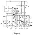
- V -> I (voltage to current) converter from Wiegerink, Seevinek, & Jager, "Offset Cancelling Circuit", JSSC, vol SC-24, pp651-658, June 1989 then provides a voltage input to the circuit, with the complete circuit shown in Fig. 6.
- module 603 provides an input signal to transistors 635 and 637, a bias signal to transistor 629, and a bias for PTAT operation to module 605.
- the amplifier represented by transistors 621, 623, 625, 627, 629, 631, and 633 sets a first bias current for a PTAT characteristic in the circuit represented by transistors 635, 633, 637, and 639.
- the output from transistor 639 then sets a bias voltage for the bases of transistors 647 and 649 in the circuit comprising transistors 641, 643, 645, 647, 649, 651 and 653, which together form the circuit developing log-linear output currents.
- Module 605 supplies a base voltage which controls the response of transistors 607 and 609.
- Transistors 607 and 609 provide collector currents in response to the base voltage from module 605 which ratios the PTAT currents in the circuits discussed above.
- module 605 also provides base voltages to transistors 613, 615, 617 and 619, which provide collector currents to apply an input signal to the base of transistor 643 and the collector of transistor 641.
- Transistor 619 also supplies a collector current to modify the response of transistor 653.
- dB-linear signals are generated at the collectors of transistors 651 and 653.
- the signal current from the collector of transistor 653 is then converted in polarity by transistors 655, 657, and 659, and the two log-linear signals discussed above are applied to transistor current clamps 665 and 667 and amplified by the pair of current sharing transistors 661 and 663.
- the desired signal Io then appears at the collector of 663. In this way, a dB-linear current is obtained from a linear input with substantially no temperature sensitivity.
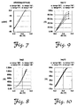
- Fig. 7 demonstrates the dB-linear characteristics of the output as a function of temperature. It can be seen that a straight line relating linear voltage to the output current in dB is obtained.
- Fig. 8 demonstrates the response of the output current to a linear voltage in terms of linear current.
- the linear voltage is related to the linear output current by an exponential line, showing again the dB-linear relationship.
- Fig. 9 demonstrates the response of a linear circuit to a linear voltage over a temperature range without PTAT compensation.
- Fig. 10 demonstrates the response of a linear circuit to a linear voltage over the same temperature range as in Fig. 9 with PTAT compensation, showing that the response is now stable as a function of temperature.
Landscapes
- Amplifiers (AREA)
- Tone Control, Compression And Expansion, Limiting Amplitude (AREA)
- Control Of Amplification And Gain Control (AREA)
Abstract
Description
Fig. 1A 150 shows a
Claims (8)
- A dB-linear amplifier (Fig. 6) for producing a logarithmic variable gain response to a control input (603) comprising:means for developing a first signal (Vo,605) proportional to the control input;means for applying the first signal to an amplifier with a natural logarithmic variable gain response (Ie,665; Ie,667; Ic,661; Ic,663) at a bias current (Ie,661; Ie,663);means for scaling the gain response to a dB-linear (Ie,665; Ie,667) value; andmeans for providing an output current (Ic,663) proportional to the first signal.
- The amplifier of claim 1 comprising:means for adjusting (643,645,647,649) the values of the bias current (Ie,661; Ie,663) and the output current (Ic,663) proportional to the first signal (Vo,605) to provide a temperature stable response.
- The amplifier of claim 1 wherein the signal is a current (Ic,609; Ic,611).
- The amplifier of claim 1 wherein the signal is a voltage (Vo,605).
- A dB-linear amplifier for producing a logarithmic variable gain response (661,663,665,667) to a control input (603) comprising:means for providing a first signal (Vo,605);means for applying said first signal (Vo,605) to an amplifying means (661,663,665,667) with a natural logarithmic variable gain response;scaling means (Ie,665; Ie,667) for scaling the gain response to a dB-linear value; andmeans for providing an output current (Ic,663) responsive to a gain means which is proportional to the input current (Ic,635) at a gain proportional to the dB-linear value of the gain means.
- The amplifier means of claim 5 comprising:adjusting means (643,645,647,649) for adjusting the value of the output current (Ic,663) proportional to the signal means (Vo,605) to provide a temperature stable response.
- The amplifier means of claim 5 wherein the signal means (Ic,607; Ic,609; Ic,611) is in the form of a current.
- The amplifier means of claim 5 wherein the signal means (Vo,605) is in the form of a voltage.
Applications Claiming Priority (2)
| Application Number | Priority Date | Filing Date | Title |
|---|---|---|---|
| US410489 | 1995-03-24 | ||
| US41048999A | 1999-09-30 | 1999-09-30 |
Publications (2)
| Publication Number | Publication Date |
|---|---|
| EP1089430A2 true EP1089430A2 (en) | 2001-04-04 |
| EP1089430A3 EP1089430A3 (en) | 2004-04-07 |
Family
ID=23624953
Family Applications (1)
| Application Number | Title | Priority Date | Filing Date |
|---|---|---|---|
| EP00115467A Withdrawn EP1089430A3 (en) | 1999-09-30 | 2000-07-18 | A dB-linear variable gain amplifier |
Country Status (2)
| Country | Link |
|---|---|
| EP (1) | EP1089430A3 (en) |
| JP (1) | JP2001119248A (en) |
Cited By (1)
| Publication number | Priority date | Publication date | Assignee | Title |
|---|---|---|---|---|
| US6791416B2 (en) | 2002-10-15 | 2004-09-14 | Agilent Technologies, Inc. | Variable gain amplifier with adjustable gain slope |
Families Citing this family (1)
| Publication number | Priority date | Publication date | Assignee | Title |
|---|---|---|---|---|
| US6748201B2 (en) * | 2002-03-28 | 2004-06-08 | Qualcomm Inc. | Gain control for communications device |
Family Cites Families (3)
| Publication number | Priority date | Publication date | Assignee | Title |
|---|---|---|---|---|
| US5200655A (en) * | 1991-06-03 | 1993-04-06 | Motorola, Inc. | Temperature-independent exponential converter |
| US5572166A (en) * | 1995-06-07 | 1996-11-05 | Analog Devices, Inc. | Linear-in-decibel variable gain amplifier |
| US5677561A (en) * | 1995-12-29 | 1997-10-14 | Maxim Integrated Products, Inc. | Temperature compensated logarithmic detector |
-
2000
- 2000-07-18 EP EP00115467A patent/EP1089430A3/en not_active Withdrawn
- 2000-09-26 JP JP2000292826A patent/JP2001119248A/en active Pending
Cited By (1)
| Publication number | Priority date | Publication date | Assignee | Title |
|---|---|---|---|---|
| US6791416B2 (en) | 2002-10-15 | 2004-09-14 | Agilent Technologies, Inc. | Variable gain amplifier with adjustable gain slope |
Also Published As
| Publication number | Publication date |
|---|---|
| JP2001119248A (en) | 2001-04-27 |
| EP1089430A3 (en) | 2004-04-07 |
Similar Documents
| Publication | Publication Date | Title |
|---|---|---|
| US3714462A (en) | Multiplier circuits | |
| US4207538A (en) | Temperature compensation circuit | |
| US4292597A (en) | Circuit for converting single-ended input signals to a pair of differential output signals | |
| US4004141A (en) | Linear/logarithmic analog multiplier | |
| US7521980B2 (en) | Process and temperature-independent voltage controlled attenuator and method | |
| JPH04506286A (en) | logarithmic amplifier | |
| NL193076C (en) | Amplifier control chain. | |
| US4301421A (en) | Direct-coupled amplifier with output offset regulation | |
| US3030022A (en) | Transistorized automatic gain control circuit | |
| JPS60216613A (en) | Variable signal gain controller | |
| US2889416A (en) | Temperature compensated transistor amplifier | |
| US3089098A (en) | Stabilized transistor amplifier | |
| US4791385A (en) | Voltage controlled amplifier for symmetrical electrical signals | |
| US3197627A (en) | Electronic function generator | |
| JP3081210B2 (en) | Linear gain amplifier | |
| US5327099A (en) | Differential stage that provides minimal offset between inputs | |
| US3300631A (en) | Analog multiplier | |
| US3480872A (en) | Direct-coupled differential input amplifier | |
| JPH08265074A (en) | Automatic gain control circuit | |
| US4975632A (en) | Stable bias current source | |
| US4181896A (en) | Device for optional dynamic compression or expansion | |
| JP2001119248A (en) | dB linear variable gain amplifier | |
| US3757239A (en) | Direct current amplifier drift reduction method | |
| JPS63283214A (en) | High frequency detecting circuit | |
| JP2001068948A (en) | MOSFET amplification circuit |
Legal Events
| Date | Code | Title | Description |
|---|---|---|---|
| PUAI | Public reference made under article 153(3) epc to a published international application that has entered the european phase |
Free format text: ORIGINAL CODE: 0009012 |
|
| AK | Designated contracting states |
Kind code of ref document: A2 Designated state(s): AT BE CH CY DE DK ES FI FR GB GR IE IT LI LU MC NL PT SE |
|
| AX | Request for extension of the european patent |
Free format text: AL;LT;LV;MK;RO;SI |
|
| RAP1 | Party data changed (applicant data changed or rights of an application transferred) |
Owner name: AGILENT TECHNOLOGIES INC. |
|
| RAP1 | Party data changed (applicant data changed or rights of an application transferred) |
Owner name: AGILENT TECHNOLOGIES INC. A DELAWARE CORPORATION |
|
| RAP1 | Party data changed (applicant data changed or rights of an application transferred) |
Owner name: AGILENT TECHNOLOGIES, INC. (A DELAWARE CORPORATION |
|
| PUAL | Search report despatched |
Free format text: ORIGINAL CODE: 0009013 |
|
| STAA | Information on the status of an ep patent application or granted ep patent |
Free format text: STATUS: THE APPLICATION HAS BEEN WITHDRAWN |
|
| AK | Designated contracting states |
Kind code of ref document: A3 Designated state(s): AT BE CH CY DE DK ES FI FR GB GR IE IT LI LU MC NL PT SE |
|
| AX | Request for extension of the european patent |
Extension state: AL LT LV MK RO SI |
|
| RIC1 | Information provided on ipc code assigned before grant |
Ipc: 7H 03G 7/06 B Ipc: 7H 03G 7/00 A |
|
| 18W | Application withdrawn |
Effective date: 20040326 |