EP1089374A2 - Planar filter and filter system - Google Patents
Planar filter and filter system Download PDFInfo
- Publication number
- EP1089374A2 EP1089374A2 EP00308030A EP00308030A EP1089374A2 EP 1089374 A2 EP1089374 A2 EP 1089374A2 EP 00308030 A EP00308030 A EP 00308030A EP 00308030 A EP00308030 A EP 00308030A EP 1089374 A2 EP1089374 A2 EP 1089374A2
- Authority
- EP
- European Patent Office
- Prior art keywords
- magnetic material
- filter
- magnetic
- input
- resonance
- Prior art date
- Legal status (The legal status is an assumption and is not a legal conclusion. Google has not performed a legal analysis and makes no representation as to the accuracy of the status listed.)
- Withdrawn
Links
- 239000002887 superconductor Substances 0.000 claims abstract description 26
- 230000035699 permeability Effects 0.000 claims abstract description 24
- 239000000758 substrate Substances 0.000 claims abstract description 18
- 230000005684 electric field Effects 0.000 claims abstract description 8
- 239000000696 magnetic material Substances 0.000 claims description 102
- 229910009493 Y3Fe5O12 Inorganic materials 0.000 claims description 5
- 229910000473 manganese(VI) oxide Inorganic materials 0.000 claims description 5
- 238000001914 filtration Methods 0.000 claims description 3
- 238000001816 cooling Methods 0.000 claims description 2
- 238000004804 winding Methods 0.000 claims 2
- 230000008878 coupling Effects 0.000 abstract description 23
- 238000010168 coupling process Methods 0.000 abstract description 23
- 238000005859 coupling reaction Methods 0.000 abstract description 23
- 239000010409 thin film Substances 0.000 abstract description 18
- 238000000034 method Methods 0.000 description 27
- 238000003780 insertion Methods 0.000 description 12
- 230000037431 insertion Effects 0.000 description 12
- 230000008859 change Effects 0.000 description 10
- 239000010408 film Substances 0.000 description 9
- 239000000463 material Substances 0.000 description 8
- 230000005415 magnetization Effects 0.000 description 5
- 238000004544 sputter deposition Methods 0.000 description 5
- 239000004020 conductor Substances 0.000 description 4
- 239000010949 copper Substances 0.000 description 4
- 230000004907 flux Effects 0.000 description 4
- 238000004891 communication Methods 0.000 description 3
- 230000007423 decrease Effects 0.000 description 3
- 230000009467 reduction Effects 0.000 description 3
- 230000002829 reductive effect Effects 0.000 description 3
- RYGMFSIKBFXOCR-UHFFFAOYSA-N Copper Chemical compound [Cu] RYGMFSIKBFXOCR-UHFFFAOYSA-N 0.000 description 2
- 229910002244 LaAlO3 Inorganic materials 0.000 description 2
- 238000005229 chemical vapour deposition Methods 0.000 description 2
- 229910052802 copper Inorganic materials 0.000 description 2
- 230000001419 dependent effect Effects 0.000 description 2
- 239000002184 metal Substances 0.000 description 2
- 229910052751 metal Inorganic materials 0.000 description 2
- 230000008569 process Effects 0.000 description 2
- 238000012545 processing Methods 0.000 description 2
- 238000000992 sputter etching Methods 0.000 description 2
- 238000007740 vapor deposition Methods 0.000 description 2
- 229910002353 SrRuO3 Inorganic materials 0.000 description 1
- 229910002370 SrTiO3 Inorganic materials 0.000 description 1
- 230000001154 acute effect Effects 0.000 description 1
- 239000013590 bulk material Substances 0.000 description 1
- 230000001413 cellular effect Effects 0.000 description 1
- 239000000919 ceramic Substances 0.000 description 1
- 238000007796 conventional method Methods 0.000 description 1
- 239000013078 crystal Substances 0.000 description 1
- 230000003247 decreasing effect Effects 0.000 description 1
- 238000013461 design Methods 0.000 description 1
- 230000006866 deterioration Effects 0.000 description 1
- 230000002542 deteriorative effect Effects 0.000 description 1
- 239000006185 dispersion Substances 0.000 description 1
- 238000011156 evaluation Methods 0.000 description 1
- 238000002474 experimental method Methods 0.000 description 1
- 230000012447 hatching Effects 0.000 description 1
- 230000002401 inhibitory effect Effects 0.000 description 1
- 238000001459 lithography Methods 0.000 description 1
- 238000004519 manufacturing process Methods 0.000 description 1
- 150000002739 metals Chemical class 0.000 description 1
- 230000002441 reversible effect Effects 0.000 description 1
- 229910052594 sapphire Inorganic materials 0.000 description 1
- 239000010980 sapphire Substances 0.000 description 1
- 238000009751 slip forming Methods 0.000 description 1
- 239000007787 solid Substances 0.000 description 1
- 238000012360 testing method Methods 0.000 description 1
- 229910021521 yttrium barium copper oxide Inorganic materials 0.000 description 1
Images




Classifications
-
- H—ELECTRICITY
- H01—ELECTRIC ELEMENTS
- H01P—WAVEGUIDES; RESONATORS, LINES, OR OTHER DEVICES OF THE WAVEGUIDE TYPE
- H01P1/00—Auxiliary devices
- H01P1/20—Frequency-selective devices, e.g. filters
- H01P1/201—Filters for transverse electromagnetic waves
- H01P1/203—Strip line filters
-
- H—ELECTRICITY
- H01—ELECTRIC ELEMENTS
- H01P—WAVEGUIDES; RESONATORS, LINES, OR OTHER DEVICES OF THE WAVEGUIDE TYPE
- H01P1/00—Auxiliary devices
- H01P1/20—Frequency-selective devices, e.g. filters
- H01P1/201—Filters for transverse electromagnetic waves
- H01P1/203—Strip line filters
- H01P1/20327—Electromagnetic interstage coupling
- H01P1/20354—Non-comb or non-interdigital filters
- H01P1/20363—Linear resonators
-
- Y—GENERAL TAGGING OF NEW TECHNOLOGICAL DEVELOPMENTS; GENERAL TAGGING OF CROSS-SECTIONAL TECHNOLOGIES SPANNING OVER SEVERAL SECTIONS OF THE IPC; TECHNICAL SUBJECTS COVERED BY FORMER USPC CROSS-REFERENCE ART COLLECTIONS [XRACs] AND DIGESTS
- Y10—TECHNICAL SUBJECTS COVERED BY FORMER USPC
- Y10S—TECHNICAL SUBJECTS COVERED BY FORMER USPC CROSS-REFERENCE ART COLLECTIONS [XRACs] AND DIGESTS
- Y10S505/00—Superconductor technology: apparatus, material, process
- Y10S505/70—High TC, above 30 k, superconducting device, article, or structured stock
-
- Y—GENERAL TAGGING OF NEW TECHNOLOGICAL DEVELOPMENTS; GENERAL TAGGING OF CROSS-SECTIONAL TECHNOLOGIES SPANNING OVER SEVERAL SECTIONS OF THE IPC; TECHNICAL SUBJECTS COVERED BY FORMER USPC CROSS-REFERENCE ART COLLECTIONS [XRACs] AND DIGESTS
- Y10—TECHNICAL SUBJECTS COVERED BY FORMER USPC
- Y10S—TECHNICAL SUBJECTS COVERED BY FORMER USPC CROSS-REFERENCE ART COLLECTIONS [XRACs] AND DIGESTS
- Y10S505/00—Superconductor technology: apparatus, material, process
- Y10S505/70—High TC, above 30 k, superconducting device, article, or structured stock
- Y10S505/701—Coated or thin film device, i.e. active or passive
-
- Y—GENERAL TAGGING OF NEW TECHNOLOGICAL DEVELOPMENTS; GENERAL TAGGING OF CROSS-SECTIONAL TECHNOLOGIES SPANNING OVER SEVERAL SECTIONS OF THE IPC; TECHNICAL SUBJECTS COVERED BY FORMER USPC CROSS-REFERENCE ART COLLECTIONS [XRACs] AND DIGESTS
- Y10—TECHNICAL SUBJECTS COVERED BY FORMER USPC
- Y10S—TECHNICAL SUBJECTS COVERED BY FORMER USPC CROSS-REFERENCE ART COLLECTIONS [XRACs] AND DIGESTS
- Y10S505/00—Superconductor technology: apparatus, material, process
- Y10S505/825—Apparatus per se, device per se, or process of making or operating same
- Y10S505/866—Wave transmission line, network, waveguide, or microwave storage device
Definitions
- the present invention relates to a planar filter constituted by disposing a filter member opposite to a tuning member, particularly to a technique of using a superconductor as a filter material for use in a communication apparatus and the like.
- a filter for extracting only a desired frequency band is an important constituting component. To realize the effective use of a frequency, and energy saving, a filter superior in attenuation property and small in insertion loss is demanded.
- a resonance element high in a Q value is necessary as a filter constituting element.
- a technique of realizing the resonance element with a high Q value there has been proposed a technique of using a superconductor as a conductor constituting the resonance element, and using a material with a very low loss such as sapphire or MgO in a substrate.
- a Q value of 10000 or more can be obtained, and a resonance property becomes very acute.
- the resonance property has to be adjusted with a high degree of accuracy when designing and making the filter.
- a technique of utilizing the aforementioned high Q value and directly filtering a high frequency signal of a GHz band is proposed in order to omit a frequency converter and realize cost reduction.
- the resonance property of the resonance element has to be highly precisely adjusted, but if an arbitrary frequency can be selected with one filter by positively changing a resonance frequency, a filter constitution can be simplified, and the cost reduction can be achieved.
- a technique of eliminating the aforementioned filter property deviation for example, there is a technique of disposing, on the resonance element, a dielectric whose permittivity changes depending upon voltage, and disposing a voltage applying electrode in the vicinity of the dielectric.
- the permittivity can locally and independently be changed.
- this enables individual and independent adjustments of (1) the resonance frequency of the resonance element, (2) coupling between the resonance elements, and (3) coupling between the resonance element and input/output portion, which are usually necessary for tuning a pass frequency band of the filter.
- the pass frequency band can variably be controlled, and a skirt property and ripple can be adjusted so that desired properties are obtained.
- the skirt property indicates rise and fall properties of both the sides of the pass frequency band
- the ripple indicates a property recess degree in the pass frequency band.
- the dielectric for changing the permittivity, and the electrode for applying the voltage are essential constituting elements, losses by the dielectric and electrode lowers the Q value of the resonance element down to several hundreds or less, and it is difficult to obtain the resonance element and filter superior in attenuation property and small in insertion loss.
- Another technique is to dispose, on a resonator of a micro-strip structure, a magnetic (YIG) plate whose permeability changes in accordance with an applied magnetic field, and uniformly apply the magnetic field to the plate from the outside in order to change the resonance frequency.
- YIG magnetic
- the present invention has been developed in consideration of the aforementioned problems, and an object thereof is to provide a planar filter which can variably control a pass frequency band with a high precision, and which is superior in skirt property and little in ripple.
- Another object of the present invention is to provide a planar filter which can individually and independently adjust a resonance frequency of a resonance element as a filter constituting component, coupling between the resonance elements, and coupling between the resonance element and an input/output portion.
- Further object of the present invention is to provide a planar filter which can tune a pass frequency band at a high speed and in a broad range with a simple constitution without sacrificing a low loss property of a superconductor.
- a planar filter comprising:
- the tuning member includes a permittivity adjusting section which can adjust an effective permittivity of at least one of a gap periphery between the resonance elements and a gap periphery between the input/output portion and the resonance element.
- the filter member is disposed opposite to the tuning member, and the tuning member can adjust the effective permittivity of at least one of the gap periphery between the resonance elements in the filter member, and the gap periphery between the input/output portion and the resonance element. Because of this, when changing the filter pass frequency band, the skirt property can be improved, and the ripple can be eliminated.
- planar filter comprising:
- the tuning member comprises:
- the tuning member including the first to third magnetic materials opposite to the filter member by disposing the tuning member including the first to third magnetic materials opposite to the filter member, and adjusting the permeability of the first to third magnetic materials, the resonance frequency, the coupling between the resonance elements, and the coupling between the resonance element and the input/output portion can variably be controlled, and the skirt property, ripple, and other filter properties can be improved.
- Fig. 1 is a view showing a structure of a first embodiment of the planar filter according to the present invention
- Fig. 2 is a sectional view in an A-A direction of Fig. 1.
- the planar filter of the present embodiment is structured in such a manner that a planar filter member 1 is disposed opposite to a similarly planar tuning member 2 via a predetermined gap.
- Fig. 1 shows a state before the filter member 1 is disposed opposite to the tuning member 2, and broken lines of Fig. 1 show vertically overlapped positions when the filter member is disposed opposite to the tuning member.
- the filter member 1 of Fig. 1 is a band pass filter of a micro-strip line structure in which a pair of input/output portions 5 formed of superconductors, and a plurality of resonance elements 6 similarly formed of the superconductors are disposed on a substrate 4 whose back surface side is a ground surface 3.
- the tuning member 2 of Fig. 1 is structured in such a manner that a plurality of dielectric thin films 8 and a plurality of electrodes 9 for applying an electric field to the dielectric thin films 8 are disposed on the surface (lower surface of Fig. 1) of a magnetic plate 7 whose permeability changes by an applied magnetic field.
- Each of the dielectric thin films 8 is disposed in a position opposite to a gap between the resonance elements 6 of the filter member 1, or a gap between the resonance element 6 of the filter member 1 and the input/output portion 5.
- the dielectric thin film 8 and electrode 9 correspond to a permittivity adjusting section
- the dielectric thin film 8 corresponds to a dielectric portion
- the electrode 9 corresponds to an electric field generating portion.
- a microwave as a filtering object is inputted to an input end of the input/output portion 5 of the filter member 1.
- a direct-current magnetic field shown by an arrow Y1 of Fig. 2 is applied from the input/output portion 5 on one end side toward the input/output portion 5 on the other end side. This magnetic field variably controls a filter pass frequency band.
- the planar filter of Fig. 1 is contained in a copper (Cu) container 11.
- the container 11 is further disposed in a Dewar 12.
- the container 11 is held in thermal contact with a cold head 14 of a refrigerator 13.
- a coil 15 for generating a magnetic field in a direction of arrow Y1 of Fig. 2 is wound around an outer wall of the container 11.
- a voltage applying power source for applying a voltage to the electrode 9 of Fig. 1 and a coil energizing power source for energizing the coil are disposed.
- a pass frequency, the skirt property or ripple of the filter of Fig. 1 are controlled.
- Fig. 3 shows an example in which an amplifier (not shown) at a subsequent stage of the filter is not contained in the Dewar 12, but the amplifier may be contained inside the Dewar 12. Moreover, for simplicity, Fig. 3 shows an example in which only one planar filter is disposed inside the Dewar 12, but a plurality of filters can be contained as shown by dotted lines of Fig. 3.
- Factors for determining the pass frequency band of the planar filter of Fig. 1 are a length of the resonance element 6, and an effective permittivity ⁇ and an effective permeability of a medium surrounding the resonance element 6.
- the skirt property and ripple are defined by an unloading Q value of the resonance element 6, coupling between the resonance elements 6, and coupling between the resonance element 6 and the input/output portion 5.
- the coupling between the resonance elements 6, and the coupling between the resonance element 6 and the input/output portion 5 are determined by gap lengths, and the effective permittivity c and effective permeability ⁇ of the medium surrounding the gaps.
- the effective permeability ⁇ entirely changes, and resonance frequencies of all the resonance elements 6 can uniformly be shifted.
- the filter pass property shifts on a frequency axis, but the coupling between the resonance elements 6, and the electromagnetic coupling between the resonance element 6 and the input/output portion 5 also change, and the filter skirt property, ripple, and other filter properties are other than designed.
- the effective permittivity ⁇ of the gap between the resonance elements 6, or the gap between the resonance element 6 and the input/output portion 5 is variably controlled, and the skirt property and ripple are adjusted.
- the dielectric with an electric field dependent permittivity with a large dielectric loss is used only in a portion disposed opposite to the gap between the resonance elements 6 or the gap between the resonance element 6 and the input/output portion 5, the unloading Q value of the resonance element 6, filter insertion loss, and skirt property are not seriously sacrificed.
- a second embodiment is characterized in that the resonance frequency of the resonance element 6, coupling between the resonance elements 6, and coupling between the resonance element 6 and the input/output portion 5 can individually and independently be adjusted.
- Fig. 4 is a view showing the second embodiment of the planar filter according to the present invention.
- Fig. 4A is a perspective view of the filter member 1; and
- Fig. 4B is a perspective view of the tuning member 2.
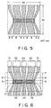
- Fig. 5 is a plan view of the tuning member 2.
- the planar filter of Fig. 4 is characterized in that the structure of the tuning member 2 is different from that of the first embodiment (Fig. 1), and the structure of the filter member 1 is similar to that of Fig. 1.
- the filter member 1 of Fig. 4A similarly as Fig. 1 is characterized in that superconductors are formed on both surfaces of the substrate 4, one surface is used as a ground conductor, the superconductor on the other surface is processed, and a pair of input/output portions 5 and the plurality of resonance elements 6 are separately formed.
- the tuning member 2 of Fig. 4B has a first magnetic material 21 disposed opposite to the gap between the input/output portion 5 and the resonance element 6, a second magnetic material 22 disposed opposite to the resonance element 6, a third magnetic material 23 disposed opposite to the gap between the resonance elements 6, fourth and seventh magnetic materials 31 and 41 disposed on both the sides of the magnetic material 21, fifth and eighth magnetic materials 32 and 42 disposed on both the sides of the magnetic material 22. sixth and ninth magnetic materials 33 and 43 disposed on both the sides of the magnetic material 23, and coils 51, 52 and 53 each connected to one end of each of the magnetic materials 31, 32 and 33.
- planar filter of Fig. 4 is, similarly as Fig. 3, contained in the copper (Cu) container 11 and disposed inside the Dewar 12.
- Fig. 6 shows that the filter member 1 is turned over and disposed opposite to the tuning member 2.
- the magnetic material 22 is disposed opposite to the resonance element 6
- the magnetic material 23 is disposed opposite to the gap between the resonance elements 6
- the magnetic material 21 is disposed opposite to the gap between the resonance element 6 and the input/output portion 5.
- the magnetic materials 21 to 23 are shown separately from the magnetic materials 31 to 33, 41 to 43 by hatching, but the materials may be formed of different members, or the same member.
- the magnetic materials 41 to 43 are disposed in such a manner that the magnetic field applied to the magnetic materials 21 to 23 is diffused in space at a place apart from the superconductors 5 and 6 on the filter member 1, and it is unnecessary to symmetrically dispose the magnetic materials 31 to 33 and the magnetic materials 41 to 43 via the magnetic materials 21 to 23.
- the magnetic materials may also be disposed on the back surface of the tuning member 2 to form a magnetic closed circuit, so that the magnetic field generated by the coil does not leak to the outside.
- a leak magnetic flux is reduced, a superconductor property can be prevented from being deteriorated due to the magnetic field, and power supplied to the coils 51 to 53 can be reduced.
- main factors for determining the filter pass frequency are the length of the resonance element 6, and effective permittivity ⁇ and effective permeability ⁇ in the vicinity of the resonance element 6.
- main factors for determining the skirt property and ripple are the Q value of the resonance element 6, coupling amount between the resonance elements 6, and coupling amount between the resonance element 6 and the input/output portion 5.
- Fig. 8 is a chart showing the frequency pass property of the filter of the present embodiment.
- the magnetic field is generated by the coils 51 and 53 of Fig. 4B, and the permeability of the magnetic materials 21 and 23 is changed to a desired value.
- the coupling between the resonance elements 6 and the coupling between the resonance element 6 and the input/output portion 5 are set to the desired values, and as shown by a solid line c of Fig. 8, a satisfactory frequency property can be obtained.
- the loss by the magnetic materials 21 to 23 is sufficiently small, the low-loss and sharp-cut filter property utilizing a superconductor characteristic is consistently maintained.
- the two-stage band pass filter has been described as an example, but the present invention can also be applied to filters with other numbers of stages.
- a filter type is not limited to the band pass filter, and the present invention can also be applied to other types such as a band reject filter, a low pass filter, and a high pass filter.
- a first concrete example described hereinafter is a concrete example of the filter of Fig. 1 described in the first embodiment, and a band pass filter of a micro-strip line structure of a 4.8 GHz band will be described.
- 0.5 mm thick LaAlO 3 was used as the substrate 4 of the filter member 1.
- a Y-based superconductor thin film was formed in 500 nm on both surfaces of the substrate 4 by a sputtering method, the superconductor thin film on one surface was used as the ground surface 3, the superconductor thin film of the other surface was processed using an ion milling method, the input/output portion 5 and a plurality of resonance elements 6 with a desired resonance frequency were formed, and the filter member 1 of the micro-strip line structure was prepared.
- Each resonance element 6 obtained a width of 170 ⁇ m, length of 8 mm, and resonance frequency of 4.8 GHz. Moreover, a 100 ⁇ m gap was disposed between the resonance elements 6, and a 70 ⁇ m gap was disposed between the resonance element 6 and the input/output portion 5.
- a 7 nm thick oxide conductive film SrRuO 3 (hereinafter referred to as the SRO film) was formed on the 0.5 mm thick magnetic plate 7 of Y 3 Fe 5 O 12 (YIG) with a saturation magnetization of 750 gausses by the sputtering method.
- the SRO film was next processed using the ion milling method, and the pair of electrodes 9 with a linear width of 10 ⁇ m and a gap of 40 ⁇ m were formed on portions opposite to a gap portion between the resonance elements 6 of the filter member 1 and a gap portion between the resonance element 6 and the input/output portion 5.
- the dielectric thin film 8 of SrTiO 3 (hereinafter referred to as the STO film) whose permittivity is dependent on the applied electric field was laminated on the portion opposite to the aforementioned gap portion in 500 nm by the sputtering method.
- the shape of the electrode 9 may be other than a two-line shape as shown in Fig. 1, or may be an inter-digital shape (comb shape) as shown in Fig. 9.
- the container 11 was disposed in the Dewar 12, connected to the refrigerator 13 which can cool to 40 K, cooling was performed to obtain 60 K, and pass property and reflection property of a microwave power were measured by a vector network analyzer.
- the applied voltage was 80 V at zero magnetic field as the initial state shown by the curve d, but when the applied voltage was 0V at the zero magnetic field, the pass band center frequency f was similar as shown by the curve d, but the property with a large ripple was obtained as shown by the curve e.
- the frequency shift in case of applying the magnetic field of 300 oersteds (Oe) was 149 MHz which was about four times the aforementioned shift, and the insertion loss increased, but was 2 dB.
- the change of the filter property by frequency tuning is adjustable by applying the voltage for the dielectric by the voltage applying electrode 9.
- the filter of the present example can arbitrarily adjust the skirt property and ripple by the voltage applying electrode 9, the pass frequency band can variably be controlled over a broad range without deteriorating the filter properties such as the skirt property and ripple.
- the dielectric thin film as a cause for deterioration of the unloading Q value is used only in the limited portions such as the gap between the resonance elements 6, the loss reduction as the characteristic of the superconductor is not sacrificed.
- the magnetic material in the tuning member 2 disposed above (or below) the filter member 1 needs to cover the entire surface of the superconductor portion of the filter member 1, and in the structure for covering only a part the filter insertion loss increased and no steep skirt property was obtained.
- a second concrete example described hereinafter is, similarly as the first concrete example, a concrete example of the first embodiment, and an example with a pass frequency band of about 2 GHz is shown.
- Fig. 11 is a view showing a structure of the second concrete example of the planar filter.
- Fig. 11A is a plan view of the filter member 1
- Fig. 11B is a plan view of the tuning member 2
- Fig. 11C is a sectional view of the planar filter of Fig. 11.
- planar filter of Fig. 11 is similar in structure and manufacture method to the planar filter of Fig. 1, except that the shape of the resonance element 6 on the filter member 1 is different.
- the resonance element 6 is lengthened by folding and disposing the resonance element 6.
- the width of the resonance element 6 on the filter member 1 was set to 170 ⁇ m, the length was 20.2 mm, the gap between the resonance elements 6 was 1.2 mm, and the gap between the resonance element 6 and the input/output portion 5 was 340 ⁇ m. As a result, the same property was obtained.
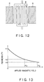
- the applicant performed the experiment on condition that the electrode 9 of the tuning member 2 is, as shown in Fig. 12, formed in the inter-digital shape, the linear width of the electrode 9 is set to 10 ⁇ m, the linear gap was 40 ⁇ m, the number of electrodes 9 between the resonance elements 6 is 24 pieces, the number of electrodes 9 between the resonance element 6 and the input/output portion 5 is six pieces, and the gap between the filter member 1 and the tuning member 2 is set to 0.3 mm.
- the insertion loss was 20 dB or more, and the filter could not bear its use.
- the band pass filter of the 2 GHz band by setting the saturation magnetization of the magnetic material to 300 gausses or less, the insertion loss obtained a practical level of 1 dB or less.
- the filter property change was similar to that of the first concrete example, but the center frequency with an applied magnetic field of 300 Oe changed by 38 MHz.
- a third concrete example described hereinafter is a concrete example of the filter of Fig. 4 described in the second embodiment.
- the planar filter shown in Fig. 4 was prepared in the following method.
- a 500 nm thick YBCO superconductor film was formed by the sputtering method, laser vapor deposition method, CVD method, or the like.
- one surface was processed by a lithography method to form the input/output portion 5 and resonance element 6, and then the back surface 13 was used as the ground surface 3 and a two-stage band pass filter of a micro-strip structure was prepared.
- the width of the resonance element 6 was set to 170 ⁇ m, the length thereof was 8 mm, the gap between the resonance elements 6 was 100 ⁇ m, and the gap between the resonance element 6 and the input/output portion 5 was 50 ⁇ m.
- the tuning member 2 shown in Fig. 4B was prepared in the following method. Over the entire top surface of the nonmagnetic ceramic substrate 4 with a longitudinal size of 35 mm, lateral size of 30 mm, thickness of 1 mm, a magnetic material composed of Y 3 Fe 5 O 12 (YIG) was formed to obtain a thickness of 100 ⁇ m by an application method.
- YIG Y 3 Fe 5 O 12
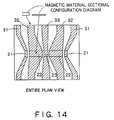
- a laser beam processor was used to process the YIG thick film with dimensions shown in Fig. 5 to obtain the form of Fig. 4B.
- the magnetic members 21 to 23, 31 to 33, 41 to 43 were continuously formed with the same materials, but may be formed with different materials.
- the magnetic field generating coils 51 to 53 as shown in Fig. 4B were disposed in the vicinity of the magnetic materials 31 to 33 using a fixing jig (not shown).
- a fixing jig (not shown).
- an inner diameter was set to 2 mm, and outer diameter was set to 4 mm, length was set to 5 mm.
- the inner diameter was set to 3 mm, outer diameter was set to 10 mm, and length was set to 10 mm.
- a conductor with a diameter of 0.1 mm was wound 800 times per 1 cm, so that the magnetic field of about 100 Oe was generated by direct-current energizing of 100 mA.
- YIG permeability changes as shown in Fig. 13. Specifically, the permeability with the zero magnetic field monotonously decreases with magnetic field application.
- the filter member 1 shown in Fig. 4A is overlapped onto the tuning member 2 shown in Fig. 4B in such a manner that the surface with the resonance element 6 formed thereon is opposite to the surface with the magnetic materials 21 to 23 formed thereon.
- the magnetic material 21 is disposed opposite to the gap between the resonance element 6 and the input/output portion 5
- the magnetic material 22 is disposed opposite to the resonance element 6, and the magnetic material 23 is disposed opposite to the gap between the resonance elements 6.
- the planar filter of the present example was prepared in this manner.
- Fig. 8 is a chart showing a pass property when the filter of the present example is cooled to 40 K.
- the center frequency f1 of the pass frequency band is 4.8 GHz
- band width is 15 MHz.
- the pass frequency band was flat and had substantially no ripple, and the insertion loss was 1 dB or less. Moreover, the property (skirt property) of the rise and fall portions on both the sides of the pass frequency band was steep. Because of this, a considerably satisfactory band pass filter property was shown.
- the initial state in which the filter property is satisfactory in all magnetic fields of zero has been described, but the constitution can also be designed in such a manner that the filter property is in the satisfactory initial state while the magnetic fields are generated by some coils.
- the permeability of YIG monotonously decreases with respect to the magnetic field as shown in Fig. 12. Therefore, it is also useful to design beforehand an initial state with an intermediate magnetic field applied thereto (e.g., a magnetic field value as shown by H2 of Fig. 12), so that adjustment is possible in a direction in which the permeability increases or decreases.
- an intermediate magnetic field applied thereto e.g., a magnetic field value as shown by H2 of Fig. 12
- a control method of trial and error can be considered in which, for example, the pass property is monitored by the network analyzer in real time.
- the YIG thickness was set to 100 ⁇ m, but actually the thickness is supposedly in a range of several tens of nanometers to several millimeters.
- the magnetic materials 21 to 23, 31 to 33, 41 to 43 are preferably formed to be as thin as possible in accordance with a necessary change amount of permeability.
- a film forming method is not limited to the application method, and with a small thickness of several micrometers or less, the film may be formed by the sputtering method, laser vapor deposition, or CVD method.
- each of the magnetic materials 21 to 23, 31 to 33, 41 to 43 is formed in a thickness of 100 ⁇ m or more, a bulk material may be placed onto the substrate 4. Moreover, when the magnetic material itself has a sufficient rigidity, the material does not have to be formed on the substrate 4, and may be prepared alone.
- the magnetic materials 21 to 23, 31 to 33, 41 to 43 are continuously prepared using the same material in the same thickness, but the thickness may be changed.
- the thickness in order to form the magnetic material 32 within the compact inner diameter of the coil, it is proposed to reduce the width of the portion in the vicinity of the coil. In this case, when the thickness is the same as that of the magnetic material 22, the sectional area of the magnetic material in the vicinity of the coils 51 to 53 becomes smaller than the sectional area of the magnetic material 22.
- the filter shown in Fig. 4 conducts the magnetic field through the magnetic materials 21 to 23, 31 to 33, 41 to 43, the number of magnetic flux lines is always kept to be constant. Moreover, since magnetic flux density is in reverse proportion to the sectional area, with the sectional area of the magnetic material 22 larger than the sectional area in the vicinity of the coils 51 to 53, the magnetic flux density is reduced, and there is a possibility that a sufficient permeability change cannot be obtained.
- a technique of increasing the thickness in the vicinity of the coils 51 to 53, so that the sectional area is unchanged as a result, is effective to obtain a sufficient permeability change.
- the sectional area in the vicinity of the coils 51 to 53 may be enlarged.
- YIG has been described as an example of the magnetic material, but the magnetic material is not limited to YIG.
- Examples of the magnetic material other than YIG include Y 3 Fe 5 O 12 , Pr 0.85 Ca 0.15 MnO 3 , and Nd 0.67 Sr 0.33 MnO 3 .
- the magnetic material has been described using the bulk plate, but a thin film obtained on the appropriate substrate 4 by various film forming methods, or a thin film formed on the filter member 1 may be used.
- a signal frequency to be filtered by the aforementioned filter is not particularly limited, but a signal up to about several tens of gigahertz can be filtered, and the present filter can therefore be applied to a frequency band utilized by a cellular phone, or the like.
Landscapes
- Physics & Mathematics (AREA)
- Electromagnetism (AREA)
- Control Of Motors That Do Not Use Commutators (AREA)
Abstract
Description
Claims (20)
- A planar filter comprising:a filter member having a plurality of resonance elements formed of superconductor films and input/output portions disposed on both the sides of said resonance elements via gaps on a dielectric substrate; anda tuning member formed of a magnetic material, said tuning member disposed opposite to said filter member via a predetermined gap and to which a direct-current magnetic field is applied,said tuning member comprising a permittivity adjusting section which adjusts an effective permittivity of at least one of a gap periphery between said resonance elements and a gap periphery between said input/output portion and said resonance element.
- The planar filter according to claim 1 wherein said permittivity adjusting section comprises:a dielectric portion disposed opposite to at least one of said gap between said resonance elements and said gap between said input/output portion and said resonance element; andan electric field generating portion for generating an electric field in said dielectric portion.
- The planar filter according to claim 2 wherein said permittivity adjusting section variably controls a voltage to be applied to said electric field generating portion to variably control the effective permittivity of at least one of said gap between said resonance elements and said gap between said resonance element and said input/output portion.
- The planar filter according to claim 1 wherein a direct-current magnetic field is applied from said input/output portion on one end side in the direction of said input/output portion on the other end side.
- The planar filter according to claim 1 wherein said filter member is a band pass filter of a micro-strip line structure in which a pair of said input/output portions formed of superconductors and said plurality of resonance elements formed of the superconductors are arranged on the substrate with a back surface side as a ground surface.
- The planar filter according to claim 1 wherein a microwave signal is inputted to an input end of said input/output portion.
- The planar filter according to claim 1 wherein said tuning member is formed using at least one of Y3Fe5O12,Pr0.85Ca0.15MnO3 and Nd0.67Sr0.33MnO3.
- A filter system comprising:a container containing the planar filter according to claim 1;a winding wound around an outer wall of said container, said winding applying a direct-current magnetic field along said gap between said filter member and said tuning member; anda refrigerator for cooling said container.
- A planar filter comprising:a filter member having a plurality of resonance elements formed of superconductor films and input/output portions disposed on both sides of said resonance elements formed via gaps on a dielectric substrate; anda tuning member disposed opposite to said filter member via a predetermined gap,said tuning member having:a first magnetic material disposed opposite to a gap between said input/output portion and said resonance element;a second magnetic material disposed opposite to each of said resonance elements;a third magnetic material disposed opposite to a gap between said resonance elements; andmagnetic field generation structure adjusting permeability of said first, said second and third magnetic materials.
- The planar filter according to claim 9 wherein said magnetic field generation structure has first, second and third coils for applying magnetic fields to said first, second and third magnetic materials independently.
- The planar filter according to claim 10 wherein said magnetic field generation structure individually controls currents for energizing said first, second and third coils to adjust a filter ripple, skirt property and a center frequency.
- The planar filter according to claim 10 wherein said filter member has n (n is an integer of 2 or more) pieces of resonance elements, andsaid tuning member has said third magnetic materials disposed opposite to (n-1) gaps between said adjacent resonance elements, and said third coils corresponding to these third magnetic materials.
- The planar filter according to claim 10 wherein said tuning member comprises:a fourth magnetic material disposed between said first coil and said first magnetic material, and connected to both of said first coil and said first magnetic material;a fifth magnetic material disposed between said second coil and said second magnetic material, and connected to both of said second coil and said second magnetic material;a sixth magnetic material disposed between said third coil and said third magnetic material, and connected to both of said third coil and said third magnetic material;a seventh magnetic material disposed on a side opposite to said fourth magnetic material by sandwiching said first magnetic material, and connected to said first magnetic material;an eighth magnetic material disposed on a side opposite to said fifth magnetic material via said second magnetic material, and connected to said second magnetic material; anda ninth magnetic material disposed on a side opposite to said sixth magnetic material by sandwiching said third magnetic material, and connected to said third magnetic material.
- The planar filter according to claim 13 wherein said first, second and third coils, said fourth, fifth and sixth magnetic materials connected to the respective coils, said first, second and third magnetic materials connected to said fourth, fifth and sixth magnetic materials, and said seventh, eighth and ninth magnetic materials connected to said first, second and third magnetic materials form closed circuits, respectively.
- The planar filter according to claim 13 wherein each of said fourth, fifth, sixth, seventh, eighth and ninth magnetic materials have a constant sectional area.
- The planar filter according to claim 15 wherein said fifth magnetic material has a narrower width and a larger thickness on a far side from said second magnetic material than those on a close side to said second magnetic material.
- The planar filter according to claim 15 wherein said fourth and sixth magnetic materials has a broader width and a smaller thickness on a far side from said first and third magnetic materials than those on a close side to said first and third magnetic materials.
- The planar filter according to claim 9 wherein said filter member is a band pass filter of a micro-strip line structure having a pair of said input/output portions formed of superconductors and said plurality of resonance elements formed of the superconductors are arranged on the substrate on which a back surface side is fixed a ground potential.
- The planar filter according to claim 9 wherein a microwave signal as a filtering object is inputted to an input end of said input/output portion.
- The planar filter according to claim 9 wherein said tuning member is formed using at least one of Y3Fe5O12,Pr0.85Ca0.15MnO3 and Nd0.67Sr0.33NnO3.
Applications Claiming Priority (2)
| Application Number | Priority Date | Filing Date | Title |
|---|---|---|---|
| JP27662699 | 1999-09-29 | ||
| JP27662699A JP3497785B2 (en) | 1999-09-29 | 1999-09-29 | Planar type filter |
Publications (2)
| Publication Number | Publication Date |
|---|---|
| EP1089374A2 true EP1089374A2 (en) | 2001-04-04 |
| EP1089374A3 EP1089374A3 (en) | 2002-10-09 |
Family
ID=17572073
Family Applications (1)
| Application Number | Title | Priority Date | Filing Date |
|---|---|---|---|
| EP00308030A Withdrawn EP1089374A3 (en) | 1999-09-29 | 2000-09-15 | Planar filter and filter system |
Country Status (6)
| Country | Link |
|---|---|
| US (1) | US6532377B1 (en) |
| EP (1) | EP1089374A3 (en) |
| JP (1) | JP3497785B2 (en) |
| KR (1) | KR100349277B1 (en) |
| CN (1) | CN1210835C (en) |
| TW (1) | TW477110B (en) |
Cited By (16)
| Publication number | Priority date | Publication date | Assignee | Title |
|---|---|---|---|---|
| EP1376754A1 (en) * | 2002-06-27 | 2004-01-02 | Harris Corporation | High efficiency resonant line |
| EP1376744A1 (en) * | 2002-06-27 | 2004-01-02 | Harris Corporation | High efficiency coupled line filters |
| US6975279B2 (en) | 2003-05-30 | 2005-12-13 | Harris Foundation | Efficient radome structures of variable geometry |
| US6982671B2 (en) | 2003-02-25 | 2006-01-03 | Harris Corporation | Slot fed microstrip antenna having enhanced slot electromagnetic coupling |
| US6985118B2 (en) | 2003-07-07 | 2006-01-10 | Harris Corporation | Multi-band horn antenna using frequency selective surfaces |
| US6992628B2 (en) | 2003-08-25 | 2006-01-31 | Harris Corporation | Antenna with dynamically variable operating band |
| US6990729B2 (en) | 2003-09-05 | 2006-01-31 | Harris Corporation | Method for forming an inductor |
| US6995711B2 (en) | 2003-03-31 | 2006-02-07 | Harris Corporation | High efficiency crossed slot microstrip antenna |
| US7006052B2 (en) | 2003-05-15 | 2006-02-28 | Harris Corporation | Passive magnetic radome |
| US7030834B2 (en) | 2003-09-03 | 2006-04-18 | Harris Corporation | Active magnetic radome |
| US7088308B2 (en) | 2003-10-08 | 2006-08-08 | Harris Corporation | Feedback and control system for radomes |
| US7158005B2 (en) | 2005-02-10 | 2007-01-02 | Harris Corporation | Embedded toroidal inductor |
| US7196607B2 (en) | 2004-03-26 | 2007-03-27 | Harris Corporation | Embedded toroidal transformers in ceramic substrates |
| US7342468B2 (en) | 2005-03-11 | 2008-03-11 | U.S. Monolithics, L.L.C. | RF filter tuning system and method |
| US8013775B2 (en) | 2007-04-30 | 2011-09-06 | Viasat, Inc. | Radio frequency absorber |
| CN115275546A (en) * | 2022-05-13 | 2022-11-01 | 成都威频科技有限公司 | YIG tunable band-stop filter of 3GHz-8GHz |
Families Citing this family (12)
| Publication number | Priority date | Publication date | Assignee | Title |
|---|---|---|---|---|
| US6778042B2 (en) * | 2000-10-30 | 2004-08-17 | Kabushiki Kaisha Toshiba | High-frequency device |
| US20040170761A1 (en) * | 2003-02-27 | 2004-09-02 | Sharp Laboratories Of America, Inc. | Precursor solution and method for controlling the composition of MOCVD deposited PCMO |
| US20050256008A1 (en) * | 2004-05-14 | 2005-11-17 | Fujitsu Limited | Superconducting filter device |
| JP4190480B2 (en) * | 2004-05-14 | 2008-12-03 | 富士通株式会社 | Superconducting filter device |
| JP4711988B2 (en) * | 2007-03-15 | 2011-06-29 | 富士通株式会社 | Superconducting disk resonator, manufacturing method thereof, and evaluation method of dielectric anisotropy |
| JP4731515B2 (en) * | 2007-03-29 | 2011-07-27 | 富士通株式会社 | Tunable filter and manufacturing method thereof |
| US8125393B2 (en) * | 2008-06-27 | 2012-02-28 | France Telecom | Reconfigurable electromagnetic antenna |
| GB2491460B (en) * | 2011-06-01 | 2017-09-06 | Filtronic Wireless Ltd | A microwave filter |
| JP5498460B2 (en) * | 2011-09-29 | 2014-05-21 | 株式会社東芝 | filter |
| CN105207639A (en) * | 2014-06-19 | 2015-12-30 | 中兴通讯股份有限公司 | Planar filter device |
| CN112002968B (en) * | 2020-08-24 | 2021-11-16 | 合肥工业大学 | Tunable terahertz band-pass filter |
| CN114976543B (en) * | 2022-07-04 | 2023-05-12 | 成都威频科技有限公司 | Interdigital YIG resonant structure and resonator |
Family Cites Families (4)
| Publication number | Priority date | Publication date | Assignee | Title |
|---|---|---|---|---|
| US5965494A (en) | 1995-05-25 | 1999-10-12 | Kabushiki Kaisha Toshiba | Tunable resonance device controlled by separate permittivity adjusting electrodes |
| DE19620932C1 (en) * | 1996-05-24 | 1997-08-21 | Bosch Gmbh Robert | Electrically tuned planar filter with ferroelectric and antiferroelectric elements |
| US6094588A (en) * | 1997-05-23 | 2000-07-25 | Northrop Grumman Corporation | Rapidly tunable, high-temperature superconductor, microwave filter apparatus and method and radar receiver employing such filter in a simplified configuration with full dynamic range |
| US5949311A (en) | 1997-06-06 | 1999-09-07 | Massachusetts Institute Of Technology | Tunable resonators |
-
1999
- 1999-09-29 JP JP27662699A patent/JP3497785B2/en not_active Expired - Fee Related
-
2000
- 2000-09-01 US US09/654,701 patent/US6532377B1/en not_active Expired - Lifetime
- 2000-09-15 EP EP00308030A patent/EP1089374A3/en not_active Withdrawn
- 2000-09-18 TW TW089119161A patent/TW477110B/en not_active IP Right Cessation
- 2000-09-27 KR KR1020000056717A patent/KR100349277B1/en not_active Expired - Fee Related
- 2000-09-29 CN CNB001292188A patent/CN1210835C/en not_active Expired - Fee Related
Cited By (22)
| Publication number | Priority date | Publication date | Assignee | Title |
|---|---|---|---|---|
| EP1376744A1 (en) * | 2002-06-27 | 2004-01-02 | Harris Corporation | High efficiency coupled line filters |
| US6741148B2 (en) | 2002-06-27 | 2004-05-25 | Harris Corporation | High efficiency coupled line filters |
| AU2003204648B2 (en) * | 2002-06-27 | 2004-12-02 | Harris Corporation | High efficiency resonant line |
| US6963259B2 (en) | 2002-06-27 | 2005-11-08 | Harris Corporation | High efficiency resonant line |
| EP1376754A1 (en) * | 2002-06-27 | 2004-01-02 | Harris Corporation | High efficiency resonant line |
| US6982671B2 (en) | 2003-02-25 | 2006-01-03 | Harris Corporation | Slot fed microstrip antenna having enhanced slot electromagnetic coupling |
| US6995711B2 (en) | 2003-03-31 | 2006-02-07 | Harris Corporation | High efficiency crossed slot microstrip antenna |
| US7006052B2 (en) | 2003-05-15 | 2006-02-28 | Harris Corporation | Passive magnetic radome |
| US6975279B2 (en) | 2003-05-30 | 2005-12-13 | Harris Foundation | Efficient radome structures of variable geometry |
| US6985118B2 (en) | 2003-07-07 | 2006-01-10 | Harris Corporation | Multi-band horn antenna using frequency selective surfaces |
| US6992628B2 (en) | 2003-08-25 | 2006-01-31 | Harris Corporation | Antenna with dynamically variable operating band |
| US7030834B2 (en) | 2003-09-03 | 2006-04-18 | Harris Corporation | Active magnetic radome |
| US7513031B2 (en) | 2003-09-05 | 2009-04-07 | Harris Corporation | Method for forming an inductor in a ceramic substrate |
| US7253711B2 (en) | 2003-09-05 | 2007-08-07 | Harris Corporation | Embedded toroidal inductors |
| US6990729B2 (en) | 2003-09-05 | 2006-01-31 | Harris Corporation | Method for forming an inductor |
| US7088308B2 (en) | 2003-10-08 | 2006-08-08 | Harris Corporation | Feedback and control system for radomes |
| US7196607B2 (en) | 2004-03-26 | 2007-03-27 | Harris Corporation | Embedded toroidal transformers in ceramic substrates |
| US7158005B2 (en) | 2005-02-10 | 2007-01-02 | Harris Corporation | Embedded toroidal inductor |
| US7342468B2 (en) | 2005-03-11 | 2008-03-11 | U.S. Monolithics, L.L.C. | RF filter tuning system and method |
| US8013775B2 (en) | 2007-04-30 | 2011-09-06 | Viasat, Inc. | Radio frequency absorber |
| CN115275546A (en) * | 2022-05-13 | 2022-11-01 | 成都威频科技有限公司 | YIG tunable band-stop filter of 3GHz-8GHz |
| CN115275546B (en) * | 2022-05-13 | 2023-05-05 | 成都威频科技有限公司 | YIG tunable band-stop filter of 3GHz-8GHz |
Also Published As
| Publication number | Publication date |
|---|---|
| CN1210835C (en) | 2005-07-13 |
| TW477110B (en) | 2002-02-21 |
| CN1290052A (en) | 2001-04-04 |
| US6532377B1 (en) | 2003-03-11 |
| JP3497785B2 (en) | 2004-02-16 |
| KR20010050671A (en) | 2001-06-15 |
| EP1089374A3 (en) | 2002-10-09 |
| KR100349277B1 (en) | 2002-08-21 |
| JP2001102808A (en) | 2001-04-13 |
Similar Documents
| Publication | Publication Date | Title |
|---|---|---|
| US6532377B1 (en) | Planar filter and filter system using a magnetic tuning member to provide permittivity adjustment | |
| JP4021844B2 (en) | Tunable ferroelectric resonator device | |
| Du et al. | Frequency tunable magnetostatic wave filters with zero static power magnetic biasing circuitry | |
| US6778042B2 (en) | High-frequency device | |
| EP1096266B1 (en) | Thin film capacitor for use with an inductor of a nuclear magnetic resonance probe coil | |
| US3681716A (en) | Tunable microminiaturized microwave filters | |
| US4853660A (en) | Integratable microwave devices based on ferromagnetic films disposed on dielectric substrates | |
| DE19733574C2 (en) | Superconducting hybrid resonator for receiving NMR signals | |
| US20030020553A1 (en) | Tunable superconductor resonator or filter | |
| US6593833B2 (en) | Tunable microwave components utilizing ferroelectric and ferromagnetic composite dielectrics and methods for making same | |
| Sharma et al. | Fabrication and characterization of microwave phase shifter in microstrip geometry with Fe film as the frequency tuning element | |
| Kagita et al. | Electrically tunable ferrite bandpass filter in X-band with wide tunability | |
| US7583167B2 (en) | High frequency magnetic thin film filter | |
| Gao et al. | Systematic design of planar millimeter-wave filters based on hexagonal barium ferrite (BaM) | |
| JP2002141705A (en) | High frequency devices | |
| Khivintsev et al. | Iron-based microstrip band-stop filters at higher microwave frequency range: Design optimization using shape anisotropy | |
| JPH0846413A (en) | Resonator and high frequency circuit element using the resonator | |
| GB2235828A (en) | Superconductive waveguide filter | |
| Nurgaliev et al. | Investigation of MW characteristics of HTS microstrip and coplanar resonators with ferrite thin-film components | |
| Du | Magnetostatic Surface Wave and Surface Acoustic Wave Devices for Tunable and Energy Efficient Radio Frequency Filters | |
| Rosenbaum | ELECTRICAL ENGINEERING DEPARTMENT WASHINGTON UNIVERSITY ST. LOUIS, MISSOURI | |
| Fukusako et al. | Microstrip superconducting resonators loaded with yttrium iron garnet single crystals | |
| Hossain | 10-section, 6-transmission zero dielectric resonator band-pass filter at 1.9 Ghz with innovative cross-coupling techniques for co-channel interference rejection | |
| Schiefer | Broadband circulators for VHF and UHF | |
| Pourush et al. | A low cost magnetically tunable microstrip ring resonator |
Legal Events
| Date | Code | Title | Description |
|---|---|---|---|
| PUAI | Public reference made under article 153(3) epc to a published international application that has entered the european phase |
Free format text: ORIGINAL CODE: 0009012 |
|
| 17P | Request for examination filed |
Effective date: 20001013 |
|
| AK | Designated contracting states |
Kind code of ref document: A2 Designated state(s): AT BE CH CY DE DK ES FI FR GB GR IE IT LI LU MC NL PT SE |
|
| AX | Request for extension of the european patent |
Free format text: AL;LT;LV;MK;RO;SI |
|
| PUAL | Search report despatched |
Free format text: ORIGINAL CODE: 0009013 |
|
| AK | Designated contracting states |
Kind code of ref document: A3 Designated state(s): AT BE CH CY DE DK ES FI FR GB GR IE IT LI LU MC NL PT SE |
|
| AX | Request for extension of the european patent |
Free format text: AL;LT;LV;MK;RO;SI |
|
| AKX | Designation fees paid |
Designated state(s): DE FR GB SE |
|
| 17Q | First examination report despatched |
Effective date: 20070125 |
|
| GRAP | Despatch of communication of intention to grant a patent |
Free format text: ORIGINAL CODE: EPIDOSNIGR1 |
|
| STAA | Information on the status of an ep patent application or granted ep patent |
Free format text: STATUS: THE APPLICATION IS DEEMED TO BE WITHDRAWN |
|
| 18D | Application deemed to be withdrawn |
Effective date: 20100226 |