EP1089186A2 - Method and apparatus for ransmiting operation packets between functional modules of a processor - Google Patents
Method and apparatus for ransmiting operation packets between functional modules of a processor Download PDFInfo
- Publication number
- EP1089186A2 EP1089186A2 EP00308366A EP00308366A EP1089186A2 EP 1089186 A2 EP1089186 A2 EP 1089186A2 EP 00308366 A EP00308366 A EP 00308366A EP 00308366 A EP00308366 A EP 00308366A EP 1089186 A2 EP1089186 A2 EP 1089186A2
- Authority
- EP
- European Patent Office
- Prior art keywords
- packet
- request
- packets
- function
- bits
- Prior art date
- Legal status (The legal status is an assumption and is not a legal conclusion. Google has not performed a legal analysis and makes no representation as to the accuracy of the status listed.)
- Granted
Links
Images


Classifications
-
- G—PHYSICS
- G06—COMPUTING OR CALCULATING; COUNTING
- G06F—ELECTRIC DIGITAL DATA PROCESSING
- G06F9/00—Arrangements for program control, e.g. control units
- G06F9/06—Arrangements for program control, e.g. control units using stored programs, i.e. using an internal store of processing equipment to receive or retain programs
- G06F9/30—Arrangements for executing machine instructions, e.g. instruction decode
- G06F9/30145—Instruction analysis, e.g. decoding, instruction word fields
-
- G—PHYSICS
- G06—COMPUTING OR CALCULATING; COUNTING
- G06F—ELECTRIC DIGITAL DATA PROCESSING
- G06F9/00—Arrangements for program control, e.g. control units
- G06F9/06—Arrangements for program control, e.g. control units using stored programs, i.e. using an internal store of processing equipment to receive or retain programs
- G06F9/30—Arrangements for executing machine instructions, e.g. instruction decode
- G06F9/30003—Arrangements for executing specific machine instructions
- G06F9/30007—Arrangements for executing specific machine instructions to perform operations on data operands
- G06F9/30032—Movement instructions, e.g. MOVE, SHIFT, ROTATE, SHUFFLE
-
- G—PHYSICS
- G06—COMPUTING OR CALCULATING; COUNTING
- G06F—ELECTRIC DIGITAL DATA PROCESSING
- G06F9/00—Arrangements for program control, e.g. control units
- G06F9/06—Arrangements for program control, e.g. control units using stored programs, i.e. using an internal store of processing equipment to receive or retain programs
- G06F9/30—Arrangements for executing machine instructions, e.g. instruction decode
- G06F9/30003—Arrangements for executing specific machine instructions
- G06F9/3004—Arrangements for executing specific machine instructions to perform operations on memory
- G06F9/30043—LOAD or STORE instructions; Clear instruction
Definitions
- the present invention relates to the transmission of packets in an integrated circuit comprising a plurality of functional modules interconnected via a packet router.
- the integrated circuit processor can comprise a plurality of functional modules connected to a packet router for transmitting and receiving the request and response packets.
- the design process is such that the architecture of a processor is designed and the functional modules which are required are determined.
- a packet protocol is developed to suit that processor. This makes it difficult to implement different designs of a similar processor, where perhaps a functional module with different interface requirements is to be added in.
- the aim is to provide a packet protocol with compact encoding but which nevertheless has artifacts providing rapid decoding of important information about the packet.
- an integrated circuit comprising: a plurality of functional modules interconnected via a packet router, each functional module having packet handling circuitry for generating and receiving packets conveyed by the packet router; wherein at least a first set of said functional modules, acting as initiator modules, have packet handling circuitry which includes request packet generation circuitry for generating request packets for implementing transactions, each request packet including a destination indicator identifying a destination of the packet and an operation field denoting the function to be implemented by the request packet, wherein the operation field comprises eight bits of which a packet type bit denotes the type of the packet, four operation family bits denote the function to be implemented by the packet and three operation qualifier bits act to qualify the function.
- a further aspect of the invention provides an integrated circuit comprising: a plurality of function modules interconnected via a packet router, each functional module having packet handling circuitry for generating and receiving packets conveyed by the packet router; wherein at least a first set of said functional modules, acting as initiator modules, have packet handling circuitry which includes request packet generation circuitry for generating request packets for implementing transactions, each request packet including a destination indicator identifying a destination of the packet and an operation field denoting the function to be implemented by the request packet, wherein the operation field comprises eight bits of which a packet type denotes the type of the packet, four operation family bits denote the function to be implemented by the packet and three operation qualifier bits act to qualify the function, and wherein a second set of said functional modules, acting as target modules, each have packet handling circuitry which includes packet receiver logic for receiving said request packets and for generating respective response packets, wherein the packet type bit distinguishes request packets and response packets.
- each request packet is a memory access operation.
- the protocol can be extended to provide additional operations as required by the particular design.
- one of said operation family bits distinguishes between primitive memory access operations involving a single request and response and compound memory access operations involving a plurality of requests and responses.
- each request packet includes a data object, the size of which is denoted by the three bit operation qualifier.
- a further embodiment of the present invention provides an initiator functional module for connection in an integrated circuit comprising: an interface for supplying and receiving packets to and from the functional module, said interface being connected to a port for connecting the functional module to a packet router; packet handling circuitry for handling said packets and including request packet generating logic which generates request packets for supply to the packet router via the interface, each request packet having a destination indicator identifying a destination of the packet and an operation field denoting the function to be implemented by the request packet, wherein the operation field comprises eight bits of which a packet type bit denotes the type of the packet, four operation family bits denote the function to be implemented by the packet and three operation qualifier bits act to qualify the function.
- a target functional module for connection in an integrated circuit comprising: an interface for supplying and receiving packets to and from the functional module, said interface being connected to a port for connecting a functional module to a packet router; packet receiver logic which is operable to receive request packets supplied from the packet router via the interface to the target functional module, each request packet having an operation field denoting the function to be implemented by the request packet, said operation field including four operation family bits denoting the function to be implemented by the packet, one of said operation family bits distinguishing between primitive memory access operations and complex memory access operations, wherein the packet receiver logic comprises means for detecting the status of said one operation family bit to determine whether the memory access operation is primitive or compound.
- a further aspect of the invention provides a method of implementing transactions in an integrated circuit comprising a plurality of functional modules interconnected via a packet router, the method comprising: at one of said functional modules acting as an initiator module, generating a request packet including a destination indicator identifying a destination of the packet and an operation field denoting the function to be implemented by the request packet, wherein the operation field comprises eight bits of which a packet type bit denotes the type of a packet, four operation family bits denote the function to be implemented by the packet and three operation qualifier bits act to qualify the function; at the destination indicated by the destination indicator, receiving said request packet and identifying the function to be implemented from the four operation family bits and the operation qualifier bits; and generating a response packet for transmission to the initiator functional module, wherein the packet type bit distinguishes between request packets and response packets.
- FIG. 1 illustrates an integrated circuit according to an embodiment of the invention.
- a CPU unit 12 is connected to a plurality of modules M by a data and address path 15 arranged to carry bit packets in parallel form.
- the modules as well as the CPU unit 12 each include packet handling circuitry 2 used in the generation and receipt of bit packets on the path 15.
- the path 15 is referred to herein as a packet router or routing bus.
- Two main types of packet are used on the data and address path 15, each including a destination indicator or address to indicate the required destination module connected to the path 15.
- the packets include request packets which are generated by an initiator module and response packets which are generated by a target module.
- a module may act as both an initiator and a target.
- Response packets are of two types, ordinary responses or error responses. These are discussed in more detail later.
- the modules M as well as the CPU unit 12 each packet handling circuitry 2 for handling packet formation and receipt of requests, ordinary responses and error responses.
- the routing bus 15 provides bi-directional connections to each module.
- the bus consists of parallel request and response buses and a dedicated control bus provided respectively for each module so as to link the modules to an arbitration unit 22.
- Each module is connected to the routing bus via a port 4 and is provided with an interface 6 incorporating a state machine so as to interchange control signals and data between the port 4 and the interface 6.
- FIG. 1A is a block diagram illustrating relevant functional components of the chip of Figure 1 to illustrate the concept of targets and initiator modules.
- the modules are labelled M1, M2, M3 and M4 and may include any of the modules M already described with reference to Figure 1.
- Modules M1 and M2 both have target and initiator functions as illustrated by the separate target and initiator parts of the interface 6 of each module.
- Module M3 acts only as an initiator and module M4 acts only as a target.
- Signals from the interfaces 6 are supplied to central control logic which forms part of the arbitration unit 22.
- the arbitration unit 22 issues request routing controls and response routing controls to the routing bus network 15.
- the various modules 14 include a debug module 30 which includes an external link 31 for transmitting packets across the chip boundary, an external memory interface EMI 32 having an external bus connection 33 leading to an external memory 50, clock circuitry 34, various peripheral interfaces 35, a peripheral component interface PCI 37 with an external connection 38, a DMA unit 25 for effecting memory accesses as well as the arbitration unit 22.
- the CPU unit 12 includes a plurality of instruction execution units 40, a plurality of registers 41, and a cache 42.
- the CPU unit 12 also includes packet handling circuitry 2 connected to the execution units 40.
- the routing bus 15 is arranged to transmit to the modules M both request and response packets for effecting memory access transactions as discussed further herein.
- packets may be generated by software as a result of instruction execution by a CPU or by hardware responsive to detection of a packet.
- Initiator modules may be autonomous and generate packets without software intervention.
- the packets may be generated on-chip and distributed on the bus 15 or generated off-chip and supplied to the on-chip bus 15 through an external connection such as the link 31 associated with the debug module 30.
- the CPU can be operated in a conventional manner receiving instructions from a program memory and effecting data read or write operations with the cache 42 on-chip. Additionally external memory accesses for read or write operations may be made through the external memory interface 32 and bus connection 33 to the external memory 50.
- the debug module 30 provides an important external communication which may be used for example in debugging procedures.
- the on-chip CPU 12 may obtain instruction .code (by memory access packets) for execution from an external source such as a debugging host 60 communicating through the link 31.
- Communications on the routing bus 15 are carried out in bit parallel format. It is possible to reduce the parallelism of packets obtained from the routing bus 15 so that they are output in bit serial format through the link 31.
- Each packet is constructed from a series of cells or tokens, the end of the packet being identified by an end of packet (eop) signal.
- the construction of the cells is discussed in more detail later.
- each packet cell comprises a number of fields which characterise the packet.
- Each packet is transmitted by a source module and is directed to a destination module.
- An initiator can issue request packets and act on response packets.
- a target can receive and act on requests and issue responses.
- a source module may be an initiator or a target depending on the nature of the packet.
- the source module uses its associated port 4 to transmit a packet onto the routing bus 15.
- the routing bus 15 arranges for the packet to be routed to the port associated with the destination module.
- the destination module then receives that packet from its associated port.
- the source and destination modules can be the same.
- a transaction is an exchange of packets that allows a module to access the state of another module.
- a transaction consists of the transfer of a request packet from a source module to a destination module, followed by the transfer of a response packet from that destination module (now acting as a responding module) back to the source module which made the original request.
- the request packet initiates a transaction and its contents determine the access to be made.
- the response packet completes the transaction and its contents indicate the result of the access.
- a response packet also indicates whether the request was valid or not. If the request was valid, a so-called ordinary response packet is sent. If the request was invalid, an error response packet is transmitted.
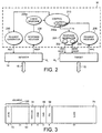
- the packet handler 2 comprises request generator logic 200, ordinary response generator logic 202, error response generator logic 204, request packet receiver logic 206, and response packet receiver logic 208. These are all under the general functional control of a control logic block 210.
- a request packet is constructed by a requesting module when that module needs to make an access to a particular target module.
- the address of the target module is recorded in the request packet destination field.
- the requesting module acts as a source of the request packet and sends that packet into the routing bus 15.
- the routing bus 15 arranges for that request packet to be routed from its source to its destination.
- the destination receives the request packet from the routing bus 15.
- the request packet receiver logic 206 checks whether or not the request is valid at 206a. If it is valid, an ordinary response packet is generated by the ordinary response generator logic 202 and the module services the requested access according to the information in the received request packet. If the request is not valid, the error response generator logic 204 generates an error response packet.
- a response packet (ordinary or error) is constructed in order to reply to the request packet.
- the module which originated the request packet is recorded in the response packet's destination field. This is discussed more fully later.
- the responding module is the source of the response packet and sends that packet onto the routing bus 15. This is done by the module interface 6.
- the response receiver logic 208 receives the response packet from the routing bus 15 and checks the response at 208a. If the response can be matched to the original request, the transaction is completed.
- Figure 3 shows the information carried by each request cell.
- Each packet is constructed from one or more cell framed using an end of packet (eop) signal.
- Each request cell comprises a 32-bit address field which indicates the destination address of the packet.
- an address comprises an 8-bit destination field 73 followed by a 24-bit offset field 63 which identifies a memory location within the destination. The offset information is present in request packets to identify the particular memory location at which the request is targeted.
- the destination field 73 is a 1-byte field used to route the packet to the destination or target module.
- a byte 74 conveys the opcode which identifies the nature of the requested access.
- the opcode can define a load word access for reading a register value and a store word access for writing a register value.
- a SRC byte 99 is a source field which identifies the source module and which is used as a return address for a response packet.
- a TID byte 98 conveys a transaction identifier which is used by the requester to associate responses with requests. The TID enables a module to identify response packets corresponding to respective request packets in cases where a plurality of request packets have been sent before response packets have been received for each request packet.
- a 64-bit data field 71 holds data to be conveyed with the request.
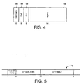
- Figure 4 illustrates the construction of a response packet cell. If the response packet contains more information than a single cell, it is constructed from a sequence of cells framed using a response end of packet (R-EOP) signal.
- the response packet includes an opcode byte 85 which denotes the nature of the requested transaction, a byte 84 which identifies the source module of the requesting packet which gave rise to the response and which acts as the return address for the response packet, a transaction identifier 98 and a data field 69.
- the opcode field 74 of a request packet has a number of different possible encodings to define the nature of the requested access. Bit 7 of the opcode is used to identify whether it is a request or a response packet however. With bit 7 set to one, the packet is a response and which bit 7 set to zero, the packet is a request. The opcode field 85 of the response packet thus has bit 7 set to one in each case. In addition, bit 0 is set to zero if the response is a ordinary response (successful transaction), and is set to one if it is an error response. Thus, the opcode field can quickly and readily identify whether a packet is a request or a response and whether the response is an ordinary response or an error response.
- a module When a module has a packet to send to another module, for example from the CPU unit 12 to the EMI module 32, it first signals this by asserting a request signal req to a dedicated line connecting that module to the central arbitration unit 22.
- M1 is the initiator module and M2 the target module. It also outputs an eight bit signal (DEST) on a destination bus to indicate to the arbitration unit 22 the intended destination of the packet it wishes to transmit.
- DEST eight bit signal
- a module M which is able to receive a packet from the routing bus 15 will assert a grant signal gnt to the central arbitration unit 22 regardless of whether a packet is available to be fed to that destination or not.
- the central arbitration unit 22 determines that a module wishes to send a packet to a destination and independently the destination has indicated that it is able to receive a packet from the bus 15, the unit 22 arranges for the transfer to take place.
- the unit 22 asserts a "grant send” signal gnt_snd to the appropriate interface 6 causing the sending module to put the packet onto the bus 15.
- the arbitration unit 22 then asserts a "send” signal snd which signals to the receiving module that it should accept the transfers currently on the bus 15.
- the packet transmission concludes when the sender asserts an "end of packet send" signal concurrently with the last transfer of packet data on the bus 15.
- Figure 5 illustrates the bit encoding of the opcode field 74 for request packets illustrated in Figure 3.
- Bit 7 identifies the packet type, that is whether the packet is a response or a request. With bit 7 set to one, this denotes that the packet is a response packet and with bit 7 set to zero this denotes that the packet is a request packet.
- Bits 0 to 3 identify the operation family which is encoded as illustrated in Table I. ⁇ 0000 ⁇ reserved ⁇ 0001 ⁇ load operation ⁇ 0010 ⁇ store operation ⁇ 0011 ⁇ reserved ⁇ 0100 ⁇ readmodwrite ⁇ 0101 ⁇ swap ⁇ 0110 ⁇ reserved ⁇ 0111 ⁇ reserved ⁇ 1000 ⁇ cache operations ⁇ 1001 ⁇ load group operations ⁇ 1010 ⁇ store group operations ⁇ 1011 - 1100 ⁇ reserved ⁇ 1101 ⁇ reserved ⁇ 1111 ⁇ user defined operation
- Each operation family may be further qualified by an operation qualifier at bits 6 to 4.
- bit 6 to 4 indicate the size of the data element the operation is working on. It uses a compact encoding 2 ⁇ n to represent the size. The values are defined as in Table II. ⁇ 000 ⁇ byte ⁇ 001 ⁇ 2 byte ⁇ 010 ⁇ 4 byte ⁇ 011 ⁇ 8 byte ⁇ 100 ⁇ 16 byte ⁇ 101 ⁇ 32 byte ⁇ 110 ⁇ 64 byte ⁇ 111 ⁇ reserved
- This encoding provides a number of advantages as mentioned below.
- bit 7 to denote the difference between request packets and response packets allows multiplexed request/response traffic to be implemented while rapidly detecting the difference between a request packet and a response packet.
- the basic memory operations have bits 2 and 3 set to zero which allows them to be rapidly determined. These basic memory operations are load and store.
- All normal memory operations including basic memory operations have bit 3 set to zero. This includes load, store, readmodwrite and swap.
- the 8 bit opcode uniquely defines the operation to be carried out by the request packet without any reference to the precise implementation of the system on which the packet is to be used.
- operation types which are supported in the described embodiment are summarised in Table III.
- operation types name qualifiers comment primitive operations load address datum, mask, data most modules typically only require the load/store 4 bytes for 32 bit systems, and load/store 8 bytes in 64 bit systems store readmodwrite swap composite operations load group address datum, mask, data this gives a mechanism for a module to enforce groupings of data which contain more than a single word store group cache operations address, address these operations are targeted as hardware assist for coherency issues flush purge locally defined user operations user defined this allows system with specific need which are not addressed by standard operations to build custom operation types which can be supported transparently by the system
- datum denotes the quantity of data/work the primitive operation is acting on.
- the qualifiers include packet qualifiers, such an address and mask as well as the operation qualifier defining the datum.
- the operations are defined in more detail in the following:
- Valid sizes for m are defined to be 2 n were n is an integer in the range 0-6.
- Valid sizes for m are defined to be 2 n where n is an integer in the range 0-6.
- Valid sizes for m are defined to be 2 n where n is an integer in the range 0-6.
- Valid sizes for m are defined to be 2 n where n is an integer in the range 0-6.
- Load a Group of words of M bytes Load Group
- the group consists of a number of elements, each of which contains m bytes, valid values for m are 2 n where n is an integer in the range 0-6.
- the group contains g* m bytes of data, and is complete when eop is asserted on the final cell of the final word to be transferred.
- the operation is a mechanism for the initiator to force the system to maintain a series of possibly unrelated operations as a single element.
- the group consists of a number of elements, each of which contains m bytes, valid values for m are 2 n where n is an integer in the range 0-6.
- the group contains g* m bytes of data, and is complete when eop is asserted on the final cell of the final word to be transferred.
- This operation is a mechanism for the initiator to force the system to maintain a series of possibly unrelated operations as a single element.
Landscapes
- Engineering & Computer Science (AREA)
- Software Systems (AREA)
- Theoretical Computer Science (AREA)
- Physics & Mathematics (AREA)
- General Engineering & Computer Science (AREA)
- General Physics & Mathematics (AREA)
- Data Exchanges In Wide-Area Networks (AREA)
Abstract
Description
| 〈0000〉 | reserved |
| 〈0001〉 | load operation |
| 〈0010〉 | store operation |
| 〈0011〉 | reserved |
| 〈0100〉 | readmodwrite |
| 〈0101〉 | swap |
| 〈0110〉 | reserved |
| 〈0111〉 | reserved |
| 〈1000〉 | cache operations |
| 〈1001〉 | load group operations |
| 〈1010〉 | store group operations |
| 〈1011 - 1100〉 | reserved |
| 〈1101〉 | reserved |
| 〈1111〉 | user defined operation |
| 〈000〉 | byte |
| 〈001〉 | 2 byte |
| 〈010〉 | 4 byte |
| 〈011〉 | 8 byte |
| 〈100〉 | 16 byte |
| 〈101〉 | 32 byte |
| 〈110〉 | 64 byte |
| 〈111〉 | reserved |
| operation types | name | qualifiers | comment |
| primitive operations | load | address datum, mask, data | most modules typically only require the load/ |
| store | |||
| readmodwrite | |||
| swap | |||
| composite operations | load group | address datum, mask, data | this gives a mechanism for a module to enforce groupings of data which contain more than a single word |
| store group | |||
| cache operations | address, address | these operations are targeted as hardware assist for coherency issues | |
| flush | |||
| purge | |||
| locally defined | user operations | user defined | this allows system with specific need which are not addressed by standard operations to build custom operation types which can be supported transparently by the system |
- address〈31:n〉
- the address of the word to be accessed
- address〈n-1:0〉
- the address of the most critical byte within the word. This ensures the system will return the critical byte as part of the first cell in the response packet.
- mask〈2^n-1:0〉
- the mask indicates which bytes with the word are significant
- r_data〈8x2n-1:0〉
- data to be transferred, the significance of bytes within this field is inferred from the mask information
- r_opcode
- result of operation
- address〈31:n〉
- the address of the word to be accessed
- address〈n-1:0〉
- the address of the most critical byte within the word
- mask〈2^n-1:0〉
- the mask indicates which bytes with the word are significant
- data〈8x2n-1:0〉
- data to be transferred
- address〈31:n〉
- the address of the word to be accessed
- address〈n-1:0〉
- the address of the most critical bytes within the word
- mask〈2^n-1:0〉
- the mask indicates which bytes with the word are significant
- data〈8x2n-1:0〉:
- data to be transferred from the initiator to the target
- r_data〈8x2n-1:0〉
- data to be transferred from the target to the initiator
- address〈31:n〉
- the address of the word to be accessed
- address〈n-1:0〉
- the address of the most critical byte within the word
- mask〈2^n-1:0〉
- the mask indicates which bytes with the word are significant
- data〈8x2n-1:0〉
- data to be transferred from the initiator to the target
- r_data〈8x2n-1:0〉:
- data to be transferred from the target to initiator
- g*address〈31:n〉:
- the address of the word to be accessed
- g*address〈n-1:0〉
- the address of the most critical byte within the word
- g*mask〈2^n-1:0〉
- the mask indicates which bytes within each word are significant
- g*r_data〈8x2n-1:0〉
- data to be transferred, the significance of bytes within this field is inferred from the mask information
- g*address〈31:n〉
- the address of the word to be accessed
- g*addregs〈n-1:0〉
- the address of the most critical byte within the word
- g*mask〈2^n-1:0〉
- the mask indicates which bytes with the word are significant
- g*r_data〈8x2n-1:0〉
- data to be transferred
| Primitive Operations | |||
| operation | 〈7〉 | bit〈6:4〉 | bit〈3:0〉 |
| reserved | - | --- | 0000 |
| | 0 | 000 | 0001 |
| load two | 0 | 001 | 0001 |
| load four | 0 | 010 | 0001 |
| load eight | 0 | 011 | 0001 |
| load sixteen | 0 | 100 | 0001 |
| load thirty-two | 0 | 101 | 0001 |
| load sixty-four | 0 | 110 | 0001 |
| - | --- | ---- | |
| reserved | 0 | --- | 0110 |
| reserved | - | --- | 0011 |
| | 0 | 000 | 0010 |
| store two | 0 | 001 | 0010 |
| store four | 0 | 010 | 0010 |
| store eight | 0 | 011 | 0010 |
| store sixteen | 0 | 100 | 0010 |
| store thirty-two | 0 | 101 | 0010 |
| store sixty-four | 0 | 110 | 0010 |
| - | --- | ---- | |
| swap four | 0 | 010 | 0101 |
| swap eight | 0 | 011 | 0101 |
| reserved | 0 | --- | 0111 |
| Compound Operations | |||
| operation | 〈7〉 | bit〈6:4〉 | bit〈3:0〉 |
| - | --- | ---- | |
| load group of | 0 | 000 | 1001 |
| load group of two | 0 | 001 | 1001 |
| load group of four | 0 | 010 | 1001 |
| load group of eight | 0 | 011 | 1001 |
| load group of sixteen | 0 | 100 | 1001 |
| load group of thirty-two | 0 | 101 | 1001 |
| load group of sixty-four | 0 | 110 | 1001 |
| store group of | 0 | 000 | 1010 |
| store group of two | 0 | 001 | 1010 |
| store group of four | 0 | 010 | 1010 |
| store group of eight | 0 | 011 | 1010 |
| store group of sixteen | 0 | 100 | 1010 |
| store group of thirty-two | 0 | 101 | 1010 |
| store group of thirty-two | 0 | 101 | 1010 |
| store group of sixty-four | 0 | 110 | 1010 |
Claims (20)
- An integrated circuit comprising:a plurality of functional modules interconnected via a packet router, each functional module having packet handling circuitry for generating and receiving packets conveyed by the packet router;
wherein at least a first set of said functional modules, acting as initiator modules, have packet handling circuitry which includes request packet generation circuitry for generating request packets for implementing transactions, each request packet including a destination indicator identifying a destination of the packet and an operation field denoting the function to be implemented by the request packet, wherein the operation field comprises eight bits of which a packet type bit denotes the type of the packet, four operation family bits denote the function to be implemented by the packet and three operation qualifier bits act to qualify the function. - An integrated circuit according to claim 1, wherein a second set of the function modules, acting as target modules, each have packet handling circuitry which includes packet receiver logic for receiving said request packets and for generating respective response packets, wherein the packet type bit distinguishes between request packets and response packets.
- An integrated circuit according to claim 1 or 2, wherein the function in each request packet is a memory access operation.
- An integrated circuit according to claim 3, wherein one of said operation family bits distinguishes between primitive memory access operations involving a single request packet and compound memory access operations involving a plurality of request packets.
- An integrated circuit according to claim 1, wherein each request packet includes a data object, the size of which is denoted by the three bit operation qualifier.
- An integrated circuit comprising:a plurality of function modules interconnected via a packet router, each functional module having packet handling circuitry for generating and receiving packets conveyed by the packet router;
wherein at least a first set of said functional module acting as initiator modules, have packet handling circuitry which includes request packet generation circuitry for generating request packets for implementing transactions, each request packet including a destination indicator identifying a destination of the packet and an operation field denoting the function to be implemented by the request packet, wherein the operation field comprises eight bits of which a packet type denotes the type of the packet, four operation family bits denotes the function to be implemented by the packet and three operation qualifier bits act to qualify the function, and
wherein a second set of said functional modules, acting as target modules, each having packet handling circuitry which includes packet receiver logic for receiving said request packets and for generating respective response packets, wherein the packet type bit distinguishes request packets and response packets. - An integrated circuit comprising:a plurality of functional modules interconnected via a packet router, each functional module having packet handling circuitry for generating and receiving packets conveyed by the packet router;
wherein each functional module has packet handling circuitry which includes request packet generation circuitry for generating request packets for implementing transactions, and packet receiver logic for receiving request packets and for generating respective response packets, each request packet including a destination indicator identifying a destination of the packet and an operation field denoting the function to be implemented by the packet, wherein the operation field comprises eight bits of which a packet type distinguishes between request packets and response packets, four operation family bits denote the function to be implemented by the packet and three operation qualifier bits act to qualify the function. - An integrated circuit according to claim 7, wherein each request packet includes a data object, the size of which is denoted by the three bit operation qualifier.
- An initiator functional module for connection in an integrated circuit comprising:an interface for supplying and receiving packets to and from the functional module, said interface being connected to a port for connecting the functional module to a packet router;packet handling circuitry for handling said packets and including request packet generating logic which generates request packets for supply to the packet router via the interface, each request packet having a destination indicator identifying a destination of the packet and an operation field denoting the function to be implemented by the request packet, wherein the operation field comprises eight bits of which a packet type bit denotes the type of the packet, four operation family bits denote the function to be implemented by the packet and three operation qualifier bits act to qualify the function.
- A target functional module for connection in an integrated circuit comprising:an interface for supplying and receiving packets to and from the functional module, said interface being connected to a port for connecting a functional module to a packet router;packet receiver logic which is operable to receive request packets supplied from the packet router via the interface to the target functional module, each request packet having an operation field denoting the function to be implemented by the request packet, said operation field including four operation family bits denoting the function to be implemented by the packet, one of said operation family bits distinguishing between primitive memory access operations and complex memory access operations, wherein the packet receiver logic comprises means for detecting the status of said one operation family bit to determine whether the memory access operation is primitive or compound.
- A target function module as claimed in claim 10, which comprises means for generating respective response packets or receipt of each request packet, wherein the operation field of both request and response packets includes a single packet type bit which distinguishes between request packets and response packets.
- A method of implementing transactions in an integrated circuit comprising a plurality of functional modules interconnected via a packet router, the method comprising:at one of said functional modules acting as an initiator module, generating a request packet including a destination indicator identifying a destination of the packet and an operation field denoting the function to be implemented by the request packet, wherein the operation field comprises eight bits of which a packet type bit denotes the type of a packet, four operation family bits denote the function to be implemented by the packet and three operation qualifier bits act to qualify the function;at the destination indicated by the destination indicator, receiving said request packet and identifying the function to be implemented from the four operation family bits and the operation qualifier bits; andgenerating a response packet for transmission to the initiator functional module, wherein the packet type bit distinguishes between request packets and response packets.
- A method according to claim 12, wherein the function in each request packet is a memory access operation.
- A method according to claim 12, wherein one of said operation family bits distinguishes between primitive memory access operations involving a single request packet and compound memory access operations involving a plurality of request packets, and wherein the method comprises detecting at the destination of the packet the status of this bit to determine whether a primitive memory access operation or a compound memory access operation is to be implemented.
- A method according to claim 12, wherein each request packet includes a data object, the size of which is denoted by the three bit operation qualifier, the method comprising at the destination of the packet, detecting the size of said data object from the three bit operation qualifier to determine how to implement the function in the request packet.
- A method according to claim 13, wherein said memory access operations include load, store, read-modify-write and swap operations.
- An integrated circuit according to claim 3, wherein the memory access operation includes cache operations.
- An integrated circuit according to claim 1, wherein the four operation family bits denote that the operation field is user defined.
- A method according to claim 13, wherein said memory access operation includes cache operations.
- A method according to claim 12, wherein said four operation family bits denote that the function defined in the operation field is user defined.
Applications Claiming Priority (2)
| Application Number | Priority Date | Filing Date | Title |
|---|---|---|---|
| US410974 | 1995-03-27 | ||
| US09/410,974 US6928073B2 (en) | 1999-10-01 | 1999-10-01 | Integrated circuit implementing packet transmission |
Publications (3)
| Publication Number | Publication Date |
|---|---|
| EP1089186A2 true EP1089186A2 (en) | 2001-04-04 |
| EP1089186A3 EP1089186A3 (en) | 2004-07-28 |
| EP1089186B1 EP1089186B1 (en) | 2007-03-21 |
Family
ID=23627029
Family Applications (1)
| Application Number | Title | Priority Date | Filing Date |
|---|---|---|---|
| EP00308366A Expired - Lifetime EP1089186B1 (en) | 1999-10-01 | 2000-09-25 | Method and apparatus for transmitting operation packets between functional modules of a processor |
Country Status (3)
| Country | Link |
|---|---|
| US (1) | US6928073B2 (en) |
| EP (1) | EP1089186B1 (en) |
| DE (1) | DE60033997D1 (en) |
Families Citing this family (3)
| Publication number | Priority date | Publication date | Assignee | Title |
|---|---|---|---|---|
| US7149212B2 (en) * | 2001-03-21 | 2006-12-12 | International Business Machines Corporation | Apparatus, method and limited set of messages to transmit data between scheduler and a network processor |
| US7512721B1 (en) | 2004-05-25 | 2009-03-31 | Qlogic, Corporation | Method and apparatus for efficient determination of status from DMA lists |
| US7729239B1 (en) * | 2004-12-27 | 2010-06-01 | Emc Corporation | Packet switching network end point controller |
Family Cites Families (76)
| Publication number | Priority date | Publication date | Assignee | Title |
|---|---|---|---|---|
| US4228496A (en) * | 1976-09-07 | 1980-10-14 | Tandem Computers Incorporated | Multiprocessor system |
| DE3584690D1 (en) | 1984-06-20 | 1992-01-02 | Convex Computer Corp | INPUT / OUTPUT BUS FOR COMPUTER. |
| US4935867A (en) | 1986-03-04 | 1990-06-19 | Advanced Micro Devices, Inc. | Signal processor memory management unit with indirect addressing using selectable offsets and modulo values for indexed address calculations |
| US4814981A (en) | 1986-09-18 | 1989-03-21 | Digital Equipment Corporation | Cache invalidate protocol for digital data processing system |
| US5483518A (en) | 1992-06-17 | 1996-01-09 | Texas Instruments Incorporated | Addressable shadow port and protocol for serial bus networks |
| JPH0666056B2 (en) | 1989-10-12 | 1994-08-24 | 甲府日本電気株式会社 | Information processing system |
| JP2835103B2 (en) * | 1989-11-01 | 1998-12-14 | 富士通株式会社 | Instruction designation method and instruction execution method |
| JPH03217949A (en) | 1990-01-23 | 1991-09-25 | Hitachi Ltd | computer system |
| US5452432A (en) | 1990-08-14 | 1995-09-19 | Chips And Technologies, Inc. | Partially resettable, segmented DMA counter |
| JP2855298B2 (en) * | 1990-12-21 | 1999-02-10 | インテル・コーポレーション | Arbitration method of interrupt request and multiprocessor system |
| JP2984463B2 (en) | 1991-06-24 | 1999-11-29 | 株式会社日立製作所 | Microcomputer |
| US5423050A (en) | 1991-11-27 | 1995-06-06 | Ncr Corporation | Intermodule test across system bus utilizing serial test bus |
| US5724549A (en) | 1992-04-06 | 1998-03-03 | Cyrix Corporation | Cache coherency without bus master arbitration signals |
| GB2266606B (en) | 1992-04-27 | 1996-02-14 | Intel Corp | A microprocessor with an external command mode |
| US5448576A (en) | 1992-10-29 | 1995-09-05 | Bull Hn Information Systems Inc. | Boundary scan architecture extension |
| JP3524110B2 (en) | 1992-11-06 | 2004-05-10 | 株式会社ルネサステクノロジ | Microcomputer system |
| JP3231429B2 (en) | 1992-11-06 | 2001-11-19 | 株式会社日立製作所 | Semiconductor integrated circuit device having central processing unit and multiplier |
| JPH06150023A (en) | 1992-11-06 | 1994-05-31 | Hitachi Ltd | Microcomputer and system thereof |
| JP3451103B2 (en) | 1992-11-27 | 2003-09-29 | 富士通株式会社 | Data communication device and method |
| US5627842A (en) | 1993-01-21 | 1997-05-06 | Digital Equipment Corporation | Architecture for system-wide standardized intra-module and inter-module fault testing |
| JP2731692B2 (en) | 1993-04-28 | 1998-03-25 | 日本電気アイシーマイコンシステム株式会社 | Debug device |
| US5598551A (en) | 1993-07-16 | 1997-01-28 | Unisys Corporation | Cache invalidation sequence system utilizing odd and even invalidation queues with shorter invalidation cycles |
| EP0636976B1 (en) | 1993-07-28 | 1998-12-30 | Koninklijke Philips Electronics N.V. | Microcontroller provided with hardware for supporting debugging as based on boundary scan standard-type extensions |
| JP3904244B2 (en) | 1993-09-17 | 2007-04-11 | 株式会社ルネサステクノロジ | Single chip data processor |
| US5914955A (en) * | 1993-10-20 | 1999-06-22 | Lsi Logic Corporation | Switched network hub on a chip |
| EP0652516A1 (en) | 1993-11-03 | 1995-05-10 | Advanced Micro Devices, Inc. | Integrated microprocessor |
| US5596734A (en) | 1993-12-17 | 1997-01-21 | Intel Corporation | Method and apparatus for programming embedded memories of a variety of integrated circuits using the IEEE test access port |
| US5828825A (en) | 1993-12-22 | 1998-10-27 | Intel Corporation | Method and apparatus for pseudo-direct access to embedded memories of a micro-controller integrated circuit via the IEEE test access port |
| US5434804A (en) | 1993-12-29 | 1995-07-18 | Intel Corporation | Method and apparatus for synchronizing a JTAG test control signal to an on-chip clock signal |
| US5488688A (en) | 1994-03-30 | 1996-01-30 | Motorola, Inc. | Data processor with real-time diagnostic capability |
| JPH07287668A (en) | 1994-04-19 | 1995-10-31 | Hitachi Ltd | Data processing device |
| GB9417602D0 (en) | 1994-09-01 | 1994-10-19 | Inmos Ltd | A controller for implementing scan testing |
| JPH08329687A (en) | 1995-06-05 | 1996-12-13 | Hitachi Ltd | Semiconductor integrated circuit |
| JP3672634B2 (en) | 1994-09-09 | 2005-07-20 | 株式会社ルネサステクノロジ | Data processing device |
| JP3740195B2 (en) | 1994-09-09 | 2006-02-01 | 株式会社ルネサステクノロジ | Data processing device |
| JP3713312B2 (en) | 1994-09-09 | 2005-11-09 | 株式会社ルネサステクノロジ | Data processing device |
| US5848247A (en) | 1994-09-13 | 1998-12-08 | Hitachi, Ltd. | Microprocessor having PC card interface |
| US5613153A (en) | 1994-10-03 | 1997-03-18 | International Business Machines Corporation | Coherency and synchronization mechanisms for I/O channel controllers in a data processing system |
| US5751621A (en) | 1994-11-17 | 1998-05-12 | Hitachi, Ltd. | Multiply-add unit and data processing apparatus using it |
| TW330265B (en) | 1994-11-22 | 1998-04-21 | Hitachi Ltd | Semiconductor apparatus |
| JP2752592B2 (en) | 1994-12-28 | 1998-05-18 | 日本ヒューレット・パッカード株式会社 | Microprocessor, signal transmission method between microprocessor and debug tool, and tracing method |
| US5778237A (en) | 1995-01-10 | 1998-07-07 | Hitachi, Ltd. | Data processor and single-chip microcomputer with changing clock frequency and operating voltage |
| US5664197A (en) | 1995-04-21 | 1997-09-02 | Intel Corporation | Method and apparatus for handling bus master channel and direct memory access (DMA) channel access requests at an I/O controller |
| US5867726A (en) | 1995-05-02 | 1999-02-02 | Hitachi, Ltd. | Microcomputer |
| US5570375A (en) | 1995-05-10 | 1996-10-29 | National Science Council Of R.O.C. | IEEE Std. 1149.1 boundary scan circuit capable of built-in self-testing |
| US5860127A (en) | 1995-06-01 | 1999-01-12 | Hitachi, Ltd. | Cache memory employing dynamically controlled data array start timing and a microcomputer using the same |
| US5774701A (en) | 1995-07-10 | 1998-06-30 | Hitachi, Ltd. | Microprocessor operating at high and low clok frequencies |
| US5708773A (en) | 1995-07-20 | 1998-01-13 | Unisys Corporation | JTAG interface system for communicating with compliant and non-compliant JTAG devices |
| US5704034A (en) * | 1995-08-30 | 1997-12-30 | Motorola, Inc. | Method and circuit for initializing a data processing system |
| US5737516A (en) | 1995-08-30 | 1998-04-07 | Motorola, Inc. | Data processing system for performing a debug function and method therefor |
| JP3655403B2 (en) | 1995-10-09 | 2005-06-02 | 株式会社ルネサステクノロジ | Data processing device |
| JP3623840B2 (en) | 1996-01-31 | 2005-02-23 | 株式会社ルネサステクノロジ | Data processing apparatus and microprocessor |
| US5950012A (en) | 1996-03-08 | 1999-09-07 | Texas Instruments Incorporated | Single chip microprocessor circuits, systems, and methods for self-loading patch micro-operation codes and patch microinstruction codes |
| US5978874A (en) | 1996-07-01 | 1999-11-02 | Sun Microsystems, Inc. | Implementing snooping on a split-transaction computer system bus |
| JPH09311786A (en) | 1996-03-18 | 1997-12-02 | Hitachi Ltd | Data processing device |
| JP3579205B2 (en) | 1996-08-06 | 2004-10-20 | 株式会社ルネサステクノロジ | Semiconductor storage device, semiconductor device, data processing device, and computer system |
| GB9617033D0 (en) | 1996-08-14 | 1996-09-25 | Int Computers Ltd | Diagnostic memory access |
| US5768152A (en) | 1996-08-28 | 1998-06-16 | International Business Machines Corp. | Performance monitoring through JTAG 1149.1 interface |
| JP3778573B2 (en) | 1996-09-27 | 2006-05-24 | 株式会社ルネサステクノロジ | Data processor and data processing system |
| JP3790307B2 (en) | 1996-10-16 | 2006-06-28 | 株式会社ルネサステクノロジ | Data processor and data processing system |
| JPH10177520A (en) | 1996-10-16 | 1998-06-30 | Hitachi Ltd | Data processor and data processing system |
| JP3641327B2 (en) | 1996-10-18 | 2005-04-20 | 株式会社ルネサステクノロジ | Data processor and data processing system |
| DE69715557T2 (en) | 1996-10-31 | 2003-06-12 | Stmicroelectronics Ltd., Almondsbury | Microcomputer with packet bus |
| GB9622686D0 (en) | 1996-10-31 | 1997-01-08 | Sgs Thomson Microelectronics | A test port controller and a method of effecting communication using the same |
| US5953538A (en) | 1996-11-12 | 1999-09-14 | Digital Equipment Corporation | Method and apparatus providing DMA transfers between devices coupled to different host bus bridges |
| US5983017A (en) | 1996-11-12 | 1999-11-09 | Lsi Logic Corporation | Virtual monitor debugging method and apparatus |
| US5771240A (en) | 1996-11-14 | 1998-06-23 | Hewlett-Packard Company | Test systems for obtaining a sample-on-the-fly event trace for an integrated circuit with an integrated debug trigger apparatus and an external pulse pin |
| US5956477A (en) | 1996-11-25 | 1999-09-21 | Hewlett-Packard Company | Method for processing information in a microprocessor to facilitate debug and performance monitoring |
| US5896550A (en) | 1997-04-03 | 1999-04-20 | Vlsi Technology, Inc. | Direct memory access controller with full read/write capability |
| US5978902A (en) | 1997-04-08 | 1999-11-02 | Advanced Micro Devices, Inc. | Debug interface including operating system access of a serial/parallel debug port |
| US5944841A (en) | 1997-04-15 | 1999-08-31 | Advanced Micro Devices, Inc. | Microprocessor with built-in instruction tracing capability |
| GB9802097D0 (en) | 1998-01-30 | 1998-03-25 | Sgs Thomson Microelectronics | DMA controller |
| GB9805482D0 (en) * | 1998-03-13 | 1998-05-13 | Sgs Thomson Microelectronics | Microcomputer |
| GB9806184D0 (en) | 1998-03-23 | 1998-05-20 | Sgs Thomson Microelectronics | A cache coherency mechanism |
| GB9809197D0 (en) * | 1998-04-29 | 1998-07-01 | Sgs Thomson Microelectronics | Microcomputer with packet translation for event packets and memory acess packets |
| GB9809203D0 (en) | 1998-04-29 | 1998-07-01 | Sgs Thomson Microelectronics | Packet distribution in a microcomputer |
-
1999
- 1999-10-01 US US09/410,974 patent/US6928073B2/en not_active Expired - Lifetime
-
2000
- 2000-09-25 DE DE60033997T patent/DE60033997D1/en not_active Expired - Lifetime
- 2000-09-25 EP EP00308366A patent/EP1089186B1/en not_active Expired - Lifetime
Also Published As
| Publication number | Publication date |
|---|---|
| US20030161308A1 (en) | 2003-08-28 |
| DE60033997D1 (en) | 2007-05-03 |
| EP1089186B1 (en) | 2007-03-21 |
| EP1089186A3 (en) | 2004-07-28 |
| US6928073B2 (en) | 2005-08-09 |
Similar Documents
| Publication | Publication Date | Title |
|---|---|---|
| US6598177B1 (en) | Monitoring error conditions in an integrated circuit | |
| US6353867B1 (en) | Virtual component on-chip interface | |
| EP4016309B1 (en) | System, apparatus and method for handling multi-protocol traffic in data link layer circuitry | |
| US6070214A (en) | Serially linked bus bridge for expanding access over a first bus to a second bus | |
| US5276684A (en) | High performance I/O processor | |
| EP1422626B1 (en) | Multi-core communications module, data communications system incorporating a multi-core communications module, and data communications process | |
| EP1032880B1 (en) | Method and apparatus for switching between source-synchronous and common clock data transfer modes in a multiple agent processing system | |
| CN100440183C (en) | Interprocessor Communication System | |
| US7640315B1 (en) | Implementing locks in a distributed processing system | |
| US6256693B1 (en) | Master/slave data bus employing undirectional address and data lines and request/acknowledge signaling | |
| AU721685B2 (en) | Bus interface control circuit | |
| US6826191B1 (en) | Packets containing transaction attributes | |
| EP1367499A1 (en) | Compute node to mesh interface for highly scalable parallel processing system | |
| US6763034B1 (en) | Connection ports for interconnecting modules in an integrated circuit | |
| US7131020B2 (en) | Distributed copies of configuration information using token ring | |
| US6590907B1 (en) | Integrated circuit with additional ports | |
| US6052754A (en) | Centrally controlled interface scheme for promoting design reusable circuit blocks | |
| US7043612B2 (en) | Compute node to mesh interface for highly scalable parallel processing system and method of exchanging data | |
| US7346072B2 (en) | Arbitration mechanism for packet transmission | |
| US6928073B2 (en) | Integrated circuit implementing packet transmission | |
| US7549091B2 (en) | Hypertransport exception detection and processing | |
| US5299196A (en) | Distributed address decoding for bus structures | |
| EP0840221A1 (en) | Microcomputer with packet bus | |
| US5944808A (en) | Partial parity correction logic | |
| JPH04102955A (en) | Interruption controller |
Legal Events
| Date | Code | Title | Description |
|---|---|---|---|
| PUAI | Public reference made under article 153(3) epc to a published international application that has entered the european phase |
Free format text: ORIGINAL CODE: 0009012 |
|
| AK | Designated contracting states |
Kind code of ref document: A2 Designated state(s): AT BE CH CY DE DK ES FI FR GB GR IE IT LI LU MC NL PT SE |
|
| AX | Request for extension of the european patent |
Free format text: AL;LT;LV;MK;RO;SI |
|
| RTI1 | Title (correction) |
Free format text: METHOD AND APPARATUS FOR TRANSMITTING OPERATION PACKETS BETWEEN FUNCTIONAL MODULES OF A PROCESSOR |
|
| PUAL | Search report despatched |
Free format text: ORIGINAL CODE: 0009013 |
|
| AK | Designated contracting states |
Kind code of ref document: A3 Designated state(s): AT BE CH CY DE DK ES FI FR GB GR IE IT LI LU MC NL PT SE |
|
| AX | Request for extension of the european patent |
Extension state: AL LT LV MK RO SI |
|
| 17P | Request for examination filed |
Effective date: 20050112 |
|
| AKX | Designation fees paid |
Designated state(s): DE FR GB IT |
|
| GRAP | Despatch of communication of intention to grant a patent |
Free format text: ORIGINAL CODE: EPIDOSNIGR1 |
|
| GRAS | Grant fee paid |
Free format text: ORIGINAL CODE: EPIDOSNIGR3 |
|
| GRAA | (expected) grant |
Free format text: ORIGINAL CODE: 0009210 |
|
| AK | Designated contracting states |
Kind code of ref document: B1 Designated state(s): DE FR GB IT |
|
| REG | Reference to a national code |
Ref country code: GB Ref legal event code: FG4D |
|
| REF | Corresponds to: |
Ref document number: 60033997 Country of ref document: DE Date of ref document: 20070503 Kind code of ref document: P |
|
| ET | Fr: translation filed | ||
| PLBE | No opposition filed within time limit |
Free format text: ORIGINAL CODE: 0009261 |
|
| STAA | Information on the status of an ep patent application or granted ep patent |
Free format text: STATUS: NO OPPOSITION FILED WITHIN TIME LIMIT |
|
| PG25 | Lapsed in a contracting state [announced via postgrant information from national office to epo] |
Ref country code: DE Free format text: LAPSE BECAUSE OF FAILURE TO SUBMIT A TRANSLATION OF THE DESCRIPTION OR TO PAY THE FEE WITHIN THE PRESCRIBED TIME-LIMIT Effective date: 20070622 |
|
| 26N | No opposition filed |
Effective date: 20071227 |
|
| PG25 | Lapsed in a contracting state [announced via postgrant information from national office to epo] |
Ref country code: IT Free format text: LAPSE BECAUSE OF FAILURE TO SUBMIT A TRANSLATION OF THE DESCRIPTION OR TO PAY THE FEE WITHIN THE PRESCRIBED TIME-LIMIT Effective date: 20070321 |
|
| GBPC | Gb: european patent ceased through non-payment of renewal fee |
Effective date: 20070925 |
|
| REG | Reference to a national code |
Ref country code: FR Ref legal event code: ST Effective date: 20080531 |
|
| PG25 | Lapsed in a contracting state [announced via postgrant information from national office to epo] |
Ref country code: FR Free format text: LAPSE BECAUSE OF NON-PAYMENT OF DUE FEES Effective date: 20071001 |
|
| PG25 | Lapsed in a contracting state [announced via postgrant information from national office to epo] |
Ref country code: GB Free format text: LAPSE BECAUSE OF NON-PAYMENT OF DUE FEES Effective date: 20070925 |