-
The present invention relates to an optical device and to a projection display
incorporating such an optical device.
-
GB 9 811 782.3 discloses a projection display in which a transmissive spatial light
modulator (SLM) in the form of a liquid crystal device (LCD) is illuminated by an
illumination source. The display is of the single panel type and includes a holographic
field element and a projection optical system. Each picture element (pixel) of the SLM
is associated with a holographic field element reflector which reflects light from the
source to the entrance aperture or pupil of a projection lens. The field function of the
display is thus incorporated in the holographic reflectors. The holographic reflectors
may be patterned in order to generate a spatially multiplexed image without the use of
absorptive colour filters.
-
This arrangement has the inconvenience that either the holographic field element
reflector in the form of a volume hologram must be incorporated immediately adjacent
the liquid crystal layer which involves manufacturing difficulties, or the holographic
reflectors may be incorporated inside the counter substrate of the SLM, which reduces
the aperture ratio and hence the display brightness.
-
Figures 1 and 2 of the accompanying drawings illustrate a known type of single panel
projection display as disclosed in H. Hamada et al, IDRC, 1994, pp 442-423 "A new
bright single panel LC-projection system without a mosaic colour filter" and in US 5
164 102. An illumination source (not shown) directs collimated white light to a set of
relatively tilted dichroic mirrors 1 for reflecting red, green and blue light with a relative
angular separation. The resulting colour component beams are directed to a microlens
array 2 disposed on the surface of a monochrome thin film transistor (TFT) LCD 3.
Each microlens of the array 2 is disposed above three pixels and focuses the red, green
and blue light beams onto the apertures of respective ones of the three pixels. The LCD
3 is of the transmissive type and the modulated light therefrom passes through a field
lens 4 and a projection lens 5 such that the image is projected onto a screen 6.
-
The size of the image of the light source produced at each pixel is determined by the
system etendue, the pitch of the LCD pixels and the thickness of the glass substrate.
Etendue is a term representing brightness at any point in a system and is defined as the
product of the beam area and solid angle of the beam divergence. For efficient coupling
of optical radiation through a projection system, the etendue should be matched at each
point through the system. Etendue mismatch causes a loss of brightness. In this
transmission panel system, the light must be focused into the relatively small aperture of
the pixel. Thus, the solid angle of the optical beam will be required to increase to
compensate in order to maintain brightness. If the glass substrate is too thick then such
a solid angle cannot be achieved by the microlenses and light is lost around the edge of
the pixel. Also, green light may spill from the aperture of the green pixel into the red
pixel and so on.
-
This type of arrangement works well for large low resolution LCD panels. However, if
it is required to provide a higher resolution display for a given size of LCD panel,
smaller pixel sizes must be provided and it may not be possible to illuminate such
smaller pixels accurately with the available etendue. Alternatively, a larger panel may
be used but this results in an increase in the bulk of the system.
-
C. Joubert et al, "Dispersive holographic microlens matrix for single LCD projection",
SPIE vol 2650 pp 243-249 discloses a projection display as illustrated in Figure 3 of the
accompanying drawings. An arc lamp 7 and parabolic reflector 8 supply collimated
white light to a phase volume hologram 9 which separates the illuminating white light
into red, green and blue beams with a small angular separation between each adjacent
pair of beams. A cylindrical microlens array 10 focuses the R,G,B beams into the
apertures of pixels in an LCD 11. This display is of the same type as that disclosed in
Hamada but with the dichroic filters replaced by the hologram 9. Accordingly, this
display suffers from the same problems associated with beam atendue, panel size and
glass thickness.
-
JP 9 015 626 A discloses a reflection mode projection display as shown in Figure 4 of
the accompanying drawings. An LCD 12 is provided with a microlens array 13 having
microlenses formed on its upper and lower surfaces. The LCD 12 comprises composite
pixels, each of which is aligned with a respective microlens 14 formed on the front
surface of the array 13. Each composite pixel comprises individual sub-pixels 15,16
and 17 aligned with respective microlenses such as 18 on the lower surface of the array
13. The sub-pixels 15,16 and 17 modulate red, green and blue light respectively, so as
to provide a single panel colour display.
-
The LCD 12 incorporates plane reflectors, each of which forms part of a respective
colour component sub-pixel. The green reflector 19 is disposed in the plane of the LCD
12 whereas the red and blue reflectors 20 and 21 are tilted in opposite directions.
-
Incident collimated colour component light beams are shown at 22B,22G and 22R.
Each of the light beams is focused by the microlens array 13 to the aperture the
corresponding sub-pixel and onto the corresponding reflector 19 to 21. The reflectors
19 to 21 have no optical power and reflect the colour component light beams
substantially back along the incident light paths. Thus, light is reflected back through
the same microlenses so that the input and output pupils are at the same location. It is
therefore necessary to provide a beam splitter in the optical system so that the output
light from the LCD 12 for projection can be separated from the path of the input light
from the illumination system. This results in increased bulk and weight together with
light and contrast losses. Also, as described hereinafter, vignetting occurs and this
results in further light losses.
-
JP 10221681 also discloses the use of a microlens array on the front surface of a
reflective LCD. Each colour component sub-pixel of the LCD has a plane reflector
which gives rise to vignetting and loss of light. Also, the microlens array is of the two
dimensional type and further loss occurs because of lens edge effects and the reduced
aperture ratio of the lenses. However, separate input and output pupils are provided so
that a beam splitter is not required.
-
US 5 825 443 discloses an arrangement which is similar to that disclosed in
JP10221681 and which therefore suffers from the same disadvantages.
-
EP 0 953 865 discloses a projection display which includes an optical modulator
comprising an LCD of reflective type and two microlens arrays. The microlens arrays
are aligned with each other and have a pitch which is three times the pitch of the
individual colour component pixels of the LCD. Each aligned pair of microlenses is
said to constitute a relay optical system having a magnification of 1. The rear electrodes
of the LCD pixels constitute plain reflectors. The use of the second microlens array
between the first microlens array and the LCD results in increased chromatic aberration
which reduces the coupling efficiency of the device. Also, there are several interfaces
between materials of different refractive index resulting in substantial losses due to
Fresnel reflection which reduce the efficiency of the device. Further, the separation
between the second array of microlenses and the reflective pixels results in loss of
brightness because of vignetting. Also, it is necessary during manufacture to align the
two microlens arrays in the counter substrate and then align this to the back plain of the
LCD, which makes the device difficult and expensive to manufacture.
-
According to a first aspect of the invention, there is provided an optical device
comprising an array of convergent microlenses disposed in front of a reflective spatial
light modulator comprising a plurality of rear reflectors, characterised in that each of the
rear reflectors has convergent optical power.
-
Each of the reflectors may be arranged to form a laterally displaced image of a
microlens aperture or a part thereof substantially at the plane of the apertures of the
microlenses of the array. The size of the image may be substantially the same as the
size of the microlens aperture or part thereof. For a predetermined direction of incident
illumination, each of the reflectors may be arranged to form an image of a first
microlens aperture or part thereof at or within a second microlens aperture or part
thereof.
-
Each of the reflectors may have a focal length substantially equal to half the optical path
between an associated one of the microlenses and the reflector.
-
Each reflector may have convergent optical power in a first direction transverse to an
optical axis of the device and may have no optical power in a second direction
transverse to the optical axis of the device and substantially perpendicular to the first
direction. Each reflector may be blazed in the second direction and the first and second
microlens apertures may comprise different parts of the same microlens aperture.
-
Each reflector may comprise a metallised relief structure. Each reflector may be
faceted.
-
Each reflector may comprise a volume holographic element.
-
Each of the microlenses may have optical power in a third direction transverse to an
optical axis of the device and no optical power in a fourth direction transverse to the
optical axis of the device and substantially perpendicular to the third direction. The
third and fourth directions may be substantially parallel to the first and second
directions, respectively. The array of microlenses may comprise a one dimensional
array of cylindrically converging microlenses.
-
Each microlens or part thereof may be associated with a respective set of the reflectors.
The spatial light modulator may comprise a plurality of composite picture elements,
each of which is associated with a respective microlens or part thereof, and comprises a
plurality of sub-picture elements, each of which is associated with a respective one of
the respective set of the reflectors. The reflectors of each set may be different from
each other and corresponding reflectors of the sets may be substantially identical to each
other.
-
The spatial light modulator may comprise a liquid crystal device. The reflectors may be
disposed between a liquid crystal layer and a substrate of the liquid crystal device. The
reflectors may planarised. As an alternative, a substrate of the liquid crystal device may
have a surface relief corresponding to the reflectors so that the liquid crystal layer has a
substantially uniform thickness.
-
According to a second aspect of the invention, there is provided a projection display
characterised by comprising a device according to the first aspect of the invention, an
illumination system for illuminating the device, and projection optics for projecting an
image corresponding to modulation of light from the illumination system by the spatial
light modulator.
-
The projection optics may have an input pupil which is laterally spaced from an output
pupil of the illumination system. The output pupil may be disposed off-axis with
respect to the device. The input pupil may be disposed on-axis or off-axis with respect
to the device.
-
The display may comprise a field lens disposed between the illumination system and
the array of microlenses.
-
The illumination system may comprise separating means for angularly separating red,
green and blue components of light for illuminating the spatial light modulator. The
separating means may comprise a plurality of relatively tilted dichroic mirrors. As an
alternative, the separating means may comprise a diffraction element, which may
comprise a blazed diffraction grating.
-
The illumination system may be arranged to illuminate the spatial light modulator with
light having a first polarisation and the projection optics may comprise a linear polariser
for passing light from the spatial light modulator having a second polarisation
substantially orthogonal to the first polarisation.
-
The device may comprise a linear polariser. The device may comprise a patterned half
wave retarder comprising first regions whose optic axes are parallel or perpendicular to
the transmission axis of the polariser and second regions whose optic axes are oriented
at 45° to the optic axes of the first regions. As an alternative, the device may comprise:
a patterned half wave retarder comprising first and second regions whose optic axis are
oriented at +22.5° and -22.5° to the transmission axis of the polariser; and an
unpatterned retarder whose optic axis is oriented at 67.5° to the transmission axis of the
polariser.
-
The illumination system may comprise a linear to circular polarisation converter, the
device may comprise a quarter waveplate and a linear polariser, and the projection
optics may comprise a circular to linear polarisation converter. Each of the linear to
circular and circular to linear polarisation converters may comprise a linear polariser
and a quarter waveplate.
-
The term "optical power" as used herein has the conventional meaning, for example as
disclosed in "Geometrical Optics and Lens Design", P Mouroulis and J McDonald,
Oxford University Press, 1997, ISBN 0-19-508931-6, pages 40 to 43. In the case of a
single spherical surface, optical power K is defined by K = c(n'-n), where c is the
curvature of the surface, n and n' represent the refractive indices before and after the
interface. For reflector systems, then n' = -n. A surface must have a non-zero K value
to possess optical power. A plane mirror has no power (c = 0).
-
The focal length f of a single spherical surface is defined as 1/K. However, the focal
length of a surface can be defined more generally and measured as the distance from the
surface to the "circle of least confusion" for a collimated illumination at the appropriate
cone angle. Thus, for "non-perfect" surfaces, there is still an imaging property of the
surface that can be measured. The focal length is defined as being the focal length
when measured in the relevant medium, for example in a counter substrate of the spatial
light modulator.
-
The circle of least confusion is defined, for example in "Optics", Hecht and Zajac,
Addison-Wesley, 1974, page 176, as being at the position at which the image blur of the
focused spot has its smallest diameter.
-
In the case of spherical or similar reflectors, there is optical power in two orthogonal
directions which are perpendicular to the optical axis of the reflector. However, a
reflector can have optical power in a single direction, for example when the reflector is
of the cylindrically converging type. In this case, the circle of least confusion is
replaced by a strip of least confusion and is at the position at which the image blur of
the focused strip has its smallest width. In this case, the optical power K is defined in
the same way as for a single spherical surface but is in one direction (in the case of a
cylindrical reflector, perpendicular to the axis of the cylinder and to the optical axis of
the reflector).
-
The focal length of the converging reflectors of the present optical device may be
substantially equal to half the optical separation of the microlenses from the reflectors
when the distance from an "input" microlens for incident light to a reflector and the
distance from the reflector to an "output" microlens for the reflected light are the same
i.e. the input and output light paths are symmetrical. In some embodiments where input
and output pupils are displaced in the second direction, the distance between the
microlens and the reflector includes the inclination of light beams through the spatial
light modulator, for example through the thickness of glass of a counter substrate. In
the case of non-symmetrical input and output paths, the focal length can be adjusted
accordingly to allow the input aperture to be imaged onto the output aperture.
-
The optimum converging reflecting surface may be an aspheric surface or a spheric
surface. Height variations of the surface may be made compatible with, for example, a
liquid crystal device manufacturing environment. For example, the surface of each
reflector may be faceted to minimise surface undulations for liquid crystal materials.
Such a surface may be fabricated from a single layer of photosensitive material by a
grey-scale masking technique.
-
In order to achieve the correct focal length, the tilt angle of the surface may vary across
the width of a sub-aperture and the tilt angle of the surface at any part of the surface of
the sub-pixel may be close to the tilt angle of the equivalent optimum surface. Thus, the
reflecting surface in a sub-pixel cannot be a single plane surface.
-
Although a diffractive surface may not have a surface curvature, nevertheless a
diffractive surface may be arranged to focus light with a focal length as defined above.
-
Such diffractive surfaces or structures thus constitute reflectors having convergent
optical power.
-
A plane surface has an infinite focal length whereas an assembly of faceted plane
surfaces with appropriate variations in tilt angles has a measurable focal length.
Accordingly, such a faceted surface also constitutes a reflector having convergent
optical power.
-
Although the device according to the first aspect of the invention may have other
applications and uses, for example in optical computing, this device is particularly
suitable for use in a projection display in accordance with the second aspect of the
invention.
-
It is thus possible to provide a projection system using a relatively large spatially
multiplexed device in a relatively compact reflective arrangement. Although colour
filtering may be provided within the device in order to provide a colour projection
display, such absorptive colour filters can be omitted so as to avoid light loss due to
absorptive filtering. High aperture ratio field reflectors can be used so as to maximise
efficiency and may be manufactured relatively easily. For example, such reflectors may
be manufactured using a metallised surface relief photoresist technique which is
compatible with existing LCD fabrication techniques.
-
It is possible to provide an arrangement in which the final pixel appearance is white
with a very high aperture ratio. Such arrangements are extendable to higher resolutions.
Arrangements using the crossed polariser mode, for example with a single large area
polariser and patterned retarder or with an input polariser in a condensing system of the
illumination system and a "crossed" output polariser at a point near a projection lens of
the projection optics, have low light absorption and can provide a higher contrast ratio
than may be achieved with standard single polariser mode arrangements. Also, front
reflection artefacts from the device may be cancelled by means of a suitable polarisation
arrangement before entering the projection optics and this provides an improved
contrast ratio.
-
The device may make use of conventional liquid crystal modes so that it is possible to
provide a low cost single panel projection system. For instance, high volume direct
view display panels, possibly with relatively small modifications, may be used and
specialist projection light valves are not required.
-
Vignetting which occurs in known types of displays can be eliminated or substantially
reduced so as to reduce light loss and improve the display brightness for a given level of
illumination. Also, input and output pupils can be separated so that a polarising beam
splitter is not necessary. This reduces the cost and bulk of a projection display and
eliminates the light losses associated with such beam splitters.
-
The use of a reflection panel allows a higher aperture ratio and hence the use of longer
focal length microlenses compared with high resolution transmission type panels for
reasons of efficient coupling of beam etendue through the system. Thus, it is more
practical to incorporate the microlenses externally of the LCD and this reduces cost and
complexity of the system
-
Some embodiments make use of a one dimensional microlens array, for example of the
cylindrically converging lenticular screen type, and this has advantages over
arrangements which use two dimensional microlens arrays. For example, a stripe LCD
panel may be used rather than a delta LCD panel. Stripe panels are more easily
available and are easier to manufacture than delta panel and non-standard pixel
configuration panels.
-
Cylindrically converging lenses are easier to tolerance with respect to alignment with a
stripe LCD panel. Also, such lenses are easy to make with substantially 100% aperture
ratio compared with the generally lower aperture ratio of two dimensional microlenses.
Further, such lenses have a reduced boundary area and this minimises scatter losses.
-
With such one dimensional microlens arrays, the output image is in the form of white
stripes. This produces an image with substantially square pixels which provides
improved viewing quality. In some embodiments, the input and output microlenses are
different parts of the same lenticule so that irregularities between input and output
surfaces may be minimised.
-
In the case where input and output pupils are separated along the cylindrical axis of the
lenticules, the visibility of facet errors in faceted reflectors is reduced.
-
The reflecting element is a less complex shape and can be made to less strict tolerance
compared with two dimensional microlenses because the imaging reflection is required
in only one dimension. Thus, increased errors in surface shape can be accepted and this
reduces complexity and cost. Also, there are fewer facet edges and this reduces light
loss caused by poor imaging performance of facets. This also reduces the probability of
degradation of alignment of the liquid crystal layer.
-
The invention will be further described, by way of example, with reference to the
accompanying drawings, in which:
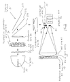
- Figure 1 is a cross-sectional diagram of a first known projection system;
- Figure 2 is a cross-sectional diagram illustrating a detail of Figure 1;
- Figure 3 is a cross-sectional diagram illustrating a second known projection system;
- Figure 4 is a cross-sectional diagram illustrating a third known projection system;
- Figure 5 is a cross-sectional diagram of a projection system constituting an embodiment
of the invention;
- Figure 6 is a cross-sectional diagram of an SLM of the system of Figure 5 constituting
an embodiment of the invention;
- Figure 7 is a cross-sectional diagram illustrating part of the system of Figure 5;
- Figures 8 and 9 are diagrams illustrating vignetting in a known projection system;
- Figure 10 is a diagram illustrating absence of vignetting in the system of Figure 5;
- Figure 11 is a diagram of part of a known type of projection system illustrating the
results of vignetting;
- Figures 12 and 13 are diagrams illustrating vignetting in systems of the type shown in
Figure 4;
- Figure 14 is a diagram illustrating absence of vignetting in the system shown in Figure
5;
- Figure 15 is a diagram illustrating the relative arrangement of pixels and lenticules in
the system of Figure 5;
- Figure 16 shows diagrammatic cross-sectional and planned views of part of the system
of Figure 5 illustrating input and output pupil separation in a first direction;
- Figure 17 is similar to 16 but illustrates a greater separation between input and output
pupils;
- Figure 18a is similar to Figure 16 but illustrates input and output pupil separation in a
second direction;
- Figures 18b and 18c are cross-sectional views on section lines B-B and C-C,
respectively, in Figure 18a illustrating imaging paths;
- Figure 19 is similar to Figure 18a, but illustrates an off-axis input pupil and an on-axis
output pupil;
- Figure 20 is a view similar to that of Figure 6, but illustrating an arrangement for
achieving the pupil arrangement of Figure 19;
- Figure 21 illustrates an arrangement of a curved reflector;
- Figure 22 illustrates an arrangement of a faceted reflector;
- Figure 23 is a cross-sectional diagram illustrating a projection system constituting
another embodiment of the invention and having a crossed polariser liquid crystal mode
of operation;
- Figure 24 is similar to Figure 23, but illustrates a different arrangement of polarisers;
- Figure 25 is a cross-sectional diagram illustrating a device constituting an embodiment
of the invention and including a patterned retarder to provide a crossed polariser liquid
crystal mode of operation;
- Figure 26 is a diagram illustrating polarising and optic axis of parts of the device shown
in Figure 25;
- Figure 27 is similar to Figure 26, but illustrates an alternative retarder arrangement;
- Figure 28 is a cross-sectional diagram illustrating off-axis input and output pupils;
- Figure 29 is a cross-sectional diagram illustrating a polarising arrangement for reducing
the effects of specular reflection.
- Figure 30 is a cross-sectional diagram of a device illustrating an alternative colour
separation arrangement;
- Figure 31 is a cross-sectional diagram illustrating an alternative illumination system
homogenising arrangement;
- Figure 32 is a diagram illustrating how etendue - modified colour images and
illumination source allow a smaller projection lens to be used;
- Figure 33 is a diagram illustrating an alternative etendue - modifying light source for
the projection system of Figure 5;
- Figures 34 to 36 illustrate a method of making reflectors for the device of Figure 6;
- Figure 37 is a cross-sectional diagram illustrating in more detail the structure of a
device as shown in Figure 6;
- Figure 38 is similar to Figure 37, but illustrates a modified structure;
- Figure 39 is a cross-sectional diagram of a device of the type shown in Figure 6
illustrating an arrangement of a microlens array; and
- Figure 40 is a cross-sectional diagram illustrating a device of the type shown in Figure
6, but modified to provide uniform liquid crystal layer thickness with curved reflectors.
-
-
Like reference numerals refer to like parts throughout the drawings.
-
The projection display shown in Figure 5 comprises a light source 30, for example in
the form of a high pressure metal-halide arc lamp, disposed within a parabolic reflector
31, which produces a substantially collimated output beam. The output beam is
supplied through a first fly-eye lens 32 and a second fly-eye lens 33 to a polarisation
conversion arrangement 34 of known type in the form of an array of polarising beam
splitters and waveplates. The light is converted by the polarisation conversion
arrangement 34 so that the output light is substantially linearly polarised in the s
polarisation state.
-
A first condenser lens 35 collects the light from the arrangement 34 and directs the light
into a substantially homogenised linearly polarised patch of light at a second condenser
lens 36 via a set of dichroic mirrors 37. The dichroic mirrors 37 comprise a mirror 37R
which reflects red light and transmits the remainder of the spectrum, a mirror 37G
which reflects green light and transmits the remainder of the spectrum, and a mirror 37B
which reflects blue light and transmits the remainder of the spectrum. Alternatively,
since only blue light passes through both of the mirrors 37R and 37G, the mirror 37B
may be a conventional silvered mirror or the like which reflects substantially all
incident light. The mirrors 37R, 37G and 37B are tilted with respect to each other by a
small angle so as to produce red, green and blue output light beams whose directions of
propagation are also angled with respect to each other.
-
The second condenser lens 36 produces an image of the first condenser lens 35 at a third
condenser lens 38. Light from the lens 38 is deflected by a plane mirror 39 towards a
reflective LCD panel 40 so that the lens 38 forms an image of the lens 36 at the panel
40. The lens 38 thus represents an illuminating light source for the panel 40. Light
from the lens 38 passes through a field lens 41, a microlens array 42 and a polariser 43
before being incident on the reflective panel 40. As an alternative, the lens 38 and the
mirror 39 may be combined into a single element in the form of a curved reflector.
-
The output pupil of the illumination source, which acts as an input pupil for the parts 40
to 43 of the display, is shown at 44. The parts 40 to 43 direct light to an output pupil
shown at 45 and representing the input pupil of a projection lens 46. The input and
output pupils 44 and 45 are laterally displaced from each other.
-
The reflective LCD panel 40, the microlens array 42 and the polariser 43 are shown in
more detail in Figure 6. The panel 40 comprises a substrate 50, a counter-substrate 51,
a liquid crystal layer 52 and a reflector arrangement 53. Electrodes, alignment layers
and other elements of the LCD panel 40 are not shown for the sake of clarity. The panel
40 is pixellated so as to comprise a plurality of composite pixels 54, each of which
comprises a red sub-pixel 55, a green sub-pixel 56 and a blue sub-pixel 57. The array
42 comprises a plurality of microlenses 58. The array 42 may comprise a two
dimensional array, for example, of square or rectangular microlenses, in which case
each microlens 58 is associated with a respective composite pixel 54. Alternatively, as
illustrated, the array 42 may comprise a one dimensional array of lenticular microlenses
so that each microlens 58 is disposed above a respective column of composite pixels 54.
-
The reflector arrangement 53 comprises a plurality of field reflectors 59, which are
shown as being faceted in Figure 6. Each field reflector 59 has convergent optical
power in a direction which is transverse to the device optical axis 60 but has no optical
power in a second direction which is transverse to the axis 60 and to the plane of Figure
6. The faceted surface has substantially the same effect as a continuous relief structure
except that the overall thickness is reduced. In the embodiment shown in Figure 6, each
of the reflectors 59 is cylindrically converging with its focal length being substantially
equal to half the distance between the reflector and the plane of the apertures of the
microlens array 42. Thus, for incident light of a predetermined angle, each reflector 59
forms an image of the aperture A of one microlens at or within the aperture B of an
adjacent microlens or, as described hereinafter, at a different part of the same microlens.
-
Figure 7 illustrates the operation for one of the component colour illuminating beams
from the input pupil 44. The microlens images the incident light to an image at the
plane of the liquid crystal layer 52 of the LCD panel 40. Each image is associated with
the aperture of a pixel and, because the red, green and blue illumination directions are
angularly separated, red, green and blue images are produced and aligned with the
apertures of respective sub-pixels 55 to 57.
-
The field reflectors 59, which are disposed immediately adjacent the liquid crystal layer
52, have optical power in the transverse direction shown in Figure 7 so that, for
example, the aperture A of an "input" microlens is imaged onto the aperture B of an
"output" microlens (which may act as an input microlens for an adjacent composite
colour pixel). The input pupil 44 is imaged to the output pupil 45.
-
Figures 8 to 10 compare the performance of the projection system illustrated in Figures
5 to 7 with that of the known system, for example as disclosed in US 5 825 443. For the
sake of clarity, these systems are illustrated in Figures 8 to 10 as the equivalent
transmission systems so that the ray paths can be more easily followed. Thus, as shown
in Figures 8 and 9, the equivalent transmission system to the reflective arrangement of
known type at the device level comprises input and output microlenses 61 and 62 and an
LCD pixel 63. In the known arrangement, the reflector has no optical power whatever
but is merely a plane mirror. Thus, for incident light passing through the centre of the
pixel 63, all of the incident light will be reflected as output light. However, for light
passing through an edge of the pixel 63 as shown in Figure 9, only part of the
illuminating light cone will be supplied to the projection lens. The remaining part of the
light cone is lost because of vignetting from the edge of the pixel.
-
Figure 10 illustrates the equivalent arrangement for the display shown in Figures 5 to 7.
In this case, the field reflector 59 is illustrated as the transmissive-mode equivalent of a
converging lens. The element 59 images the aperture of the input microlens 61 onto the
aperture of the output microlens 62 and the effect of this is to ensure that substantially
all of the input cone of illuminating light passes through the microlens 62 and hence to
the projection lens so that light loss caused by vignetting is greatly reduced or
eliminated. Accordingly, for a given illuminating power, a brighter display may be
produced.
-
Figure 11 illustrates the effect of vignetting on a known type of system which is similar
to that shown in Figure 7 but in which the field reflectors with optical power are
replaced by plane reflectors with no optical power. The effect of vignetting is to lose
reflected light to an auxiliary exit pupil 64. Such light is not gathered by the projection
optics whose input pupil corresponds to the output pupil 45. Thus, the brightness of the
image produced by the display is reduced. If the projection lens is large enough to
capture the light from the adjacent pupil 64 as well as the main pupil 45, then the light
from adjacent composite colour pixels will appear to come from the same microlens and
will then be mixed on the projection screen so that the modulation transfer function of
the display will be degraded. Additionally, such a high numerical aperture of capture of
the projection lens is unlikely to produce satisfactory aberrational performance.
-
Figures 12 to 14 are similar to Figures 8 to 10, respectively, but compare the
performance of the display shown in Figures 5 to 7 with the known type of display
shown in Figure 4 having the inclined plane reflectors 19 to 21. Thus, the edge sub-pixels
have the tilted plane mirrors 20 and 21 which steer light back towards the centre
of the output pupil. Figure 13 illustrates that vignetting still occurs for this system
whereas, as shown in Figure 14, the field reflector 59 with convergent optical power
substantially removes or avoids this effect.
-
Figure 15 illustrates the relative lateral alignment of the composite pixel 54 and the
colour component sub-pixels 55 to 57 with the microlenses 58 of the array 42. The
pixels and sub-pixels are arranged as a rectangular array of rows and columns and the
lenticules of the array 42 are arranged in the column direction. Adjacent pairs of
lenticules 42 are arranged symmetrically over a respective column of composite pixels
54. Such an arrangement produces input and output pupils which are "horizontally"
separated by one pupil separation as illustrated in Figure 16. Each reflector 59 forms an
image of the aperture A of part of one microlens at the aperture B of the adjacent
microlens. The remaining optical system of the display forms the output pupil
immediately adjacent the input pupil 46.
-
Figure 17 illustrates a modified arrangement in which the input and output pupils 44
and 45 are separated by two pupil separations or pitches. In this case, each reflector 59
forms an image of the aperture A at the aperture B of the next but one microlens.
-
Figures 18a to 18c illustrate an alternative arrangement in which the input and output
pupils are "vertically" separated by an arbitrary separation. In this case, each reflector
images a microlens aperture back onto the same microlens aperture as shown in Figure
18b but at a spacing in the direction of the cylindrical axis of the microlenses as shown
in Figure 18c.
-
Figure 19 illustrates a modified arrangement of the type shown in Figure 18 in which an
off-axis illumination results in a central output pupil. In order to achieve this, the
reflectors 59 are blazed in the second direction i.e. that perpendicular to the direction in
which they have optical power. An arrangement for achieving such off-axis input on-axis
output is illustrated in Figure 20.
-
Figure 21 illustrates one possible arrangement of the field reflectors 59, in which the
reflectors for the three sub-pixels 55 to 57 of a composite pixel are combined into a
single curved reflector surface. Figure 21 also illustrates at 59' how the single curved
surface may be replaced by an equivalent faceted surface.
-
Figure 22 illustrates another field reflector arrangement comprising an array of blazed
plane surfaces, each of which has a different tilt. There is a plurality of such surfaces
across the aperture and the effect of this is to provide a reflector of focal length such
that a focused image is produced at or near the aperture of the output microlens.
-
The display shown in Figure 23 differs from that shown in Figure 5 in that the polariser
43 is omitted and individual polarisers 65 and 66 are provided (the dichroic mirrors are
not shown in Figure 23 for the sake of clarity). The polariser 65 is located at the input
aperture and performs a "clean-up" function to ensure that the illuminating light which
is incident on the reflective panel 40 is linearly polarised to a high degree. The polariser
66 is located at the output pupil and acts as an analyser for light from the liquid crystal
pixels. The polarising axes of the polarisers 65 and 66 are orthogonal to each other so
as to provide a crossed polariser liquid crystal mode of operation. In this case, the
polariser 43 may be omitted.
-
The optical intensity at the polarisers 65 and 66 may be sufficiently high to degrade the
performance of these polarisers. Figure 24 shows an alternative arrangement in which
the polariser 65 is located in the illumination system where light intensity is much less.
Similarly, the analyser 66 is disposed at the output of the projection lens 46 where the
light intensity is much less. In this case, the analyser 66 comprises a non-absorbing
polariser 67 and an absorbing polariser 68. Again, the polariser 43 may be omitted
-
The display shown in Figure 5 has the LCD panel 40 operating in the single polariser
mode. However, such an arrangement may have limited contrast performance and may
be modified to operate as a crossed polariser device as shown in Figure 25. In this case,
a patterned half wave retarder 70, for example of the type disclosed in GB 2 326 729
and EP 0 887 667, is disposed between the polariser 43 and the liquid crystal layer 52.
-
Figure 26 illustrates the relative orientations of the transmission direction of the
polariser 43 and the optic axes of the strips of the patterned retarder 70. The effective
polarisation orientations of the light passing through the polariser 43 and the retarder 70
are illustrated at 71. The transmission direction of the polariser 43 is parallel to the
optic axes of a first set of strips of the patterned retarder whereas the optic axes of a
second set of strips, each of which is disposed between two of the first set of strips, is
oriented at 45° to the transmission direction of the polariser 43. Thus, light passing
through the first strips such as 72 has its polarisation direction unchanged whereas light
passing through the second strips such as 73 has its polarising direction rotated through
90°.
-
As shown in Figure 25, the strips 72 and 73 are aligned with respective microlenses 42.
Incident light for the liquid crystal layer 52 passes through, for example, a first strip 72
whereas the reflected light passes through the adjacent strip 73. This arrangement is
equivalent to a liquid crystal mode with crossed polarisers and thus provides improved
contrast ratio performance.
-
Figure 27 illustrates an alternative arrangement in which the patterned retarder 70 has
alternate optic axes oriented at +22.5° and -22.5° with respect to the transmission
direction of the polariser 43. The retarder 70 is disposed between the polariser 43 and
an unpatterned half wave retarder 75 whose optic axis is oriented at +67.5° to the
transmission direction of the polariser 43. The operation of this arrangement is
substantially the same as that illustrated in Figure 26 but the performance is more
achromatic.
-
Figure 28 illustrates a projection display which differs from that shown in Figures 5 to 7
in that the input and output pupils 44 and 45 are disposed off-axis with respect to the
panel 40. An off-axis field lens 41 is used in this arrangement.
-
An advantage of this arrangement is that specular reflection occurring within the device
40 and the associated parts are directed away from the output pupil 45. For example,
specular reflections 76 from the input surface of the field lens 41 are illustrated in
Figure 28 and are directed away from the projection lens pupil which coincides with the
output pupil 45. Thus, such an off-axis arrangement reduces the amount of stray light
entering the projection lens and has an improved contrast ratio.
-
In this respect, the crossed polariser arrangements illustrated in Figures 23 and 24
provide good rejection of stray light because specularly reflected stray light has
substantially the same polarisation as the illuminating light and is extinguished by the
output polariser.
-
Figure 29 illustrates another arrangement for improving the contrast ratio by reducing
the effects of Fresnel reflections at the field lens 41 and the microlens array 42 in a
single-polarisation type of configuration. A linear polariser 78 and a quarter waveplate
79 are disposed between the reflective panel 40 and the microlens array 42. A linear to
circular polarisation converter comprising a linear polariser 80 and a quarter waveplate
81 are disposed at the input pupil whereas a circular to linear polarisation converter
comprising a quarter waveplate 82 and a linear polariser 83 are disposed at the output
pupil.
-
Figure 30 illustrates an arrangement which differs from that shown in Figure 5 in that
the dichroic mirrors 37 for separating the colour components of illuminating light are
omitted and colour separation is performed by a blazed diffraction grating 85 or
equivalent holographic optical element disposed between the field lens 41 and the
microlens array 42. Light incident on the grating 85 is split into its spectral component
directions by the dispersion of the diffraction grating. Upon reflection from the panel
50, the dispersively separated light is recombined by the same transmission grating to
produce a white image of the illumination source at the projection lens pupil. Such an
arrangement does not increase the optical etendue of the light or separate the colour
pupils in the aperture of the projection lens (separation of colour pupils results in
different aberrations for the red, green and blue components).
-
Figure 31 illustrates a projection display which differs from that shown in Figure 5 in
that the parts 32,33 and 35 are replaced by an integrated rod 86 for homogenising the
output of the light source so as to produce uniform illumination of the panel 40. The
input aperture of the glass rod 86 is circular whereas the output aperture is rectangular
with an aspect ratio which matches that of the panel 40.
-
When dichroic mirrors are used to separate the light into three distinct colour beams, the
numerical aperture of the optical system must be increased to capture the increased
optical etendue of the beam to avoid degrading the system efficiency. If the shape of
the source is not altered, then the f-number of the projection lens must grow by a factor
of three to capture all the light. Figure 32 illustrates the cross-sectional area of the
white illuminating beam 90 and the reduction in the f number to capture the three
adjacent colour component beams is illustrated at 91.
-
By altering the shape of the source so as to be rectangular and so that the aspect ratio of
each of the colour images is 3:1, the entrance pupil of the projection lens can be more
efficiently filled so that the reduction in the f number of the projection lens is reduced to
approximately 2.2 as shown at 92.
-
Etendue modification of the illumination source may be performed as illustrated in
Figure 33. An homogeniser 94 comprises two sets of lenslet arrays 95 and 96, each
comprising off-centered or eccentric optical surfaces. The first array 95 comprises
apertures whose shape is substantially identical to that of the panel 40 and the optical
centres create an array of closely packed images of the light emitter 30 at the plane of
the second array 96. The array 96 comprises a respective lens located at each light
emitter image and with an optical centre whose position is determined by drawing a
straight line between the physical centre of the rectangular image of the corresponding
first lenslet of the array 95 and the physical centre of the intermediate rectangular image
of the first lenslet aperture produced at a relay lens 97. The etendue modified image of
the source is illustrated at 98.
-
Although not shown in Figure 33, the etendue modification may be performed with the
polarisation conversion in a combined arrangement.
-
As shown in Figure 21, the reflectors 59 may be formed as continuous surfaces.
However, reflectors of this type may require unacceptably large depth, for example
resulting in excessive variations in thickness of the liquid crystal layer or in
requirements for relatively deep planarisation. Figure 22 illustrates an alternative
arrangement in which the reflectors are faceted so as to limit the depth to a
predetermined maximum value.
-
Figures 34 to 36 illustrate a method of making a faceted reflector of the type shown in
Figure 22. Figure 34 illustrates a grey-scale mask 99 which, for example, is made
photographically in any suitable way. As shown in Figure 35, the mask 99 is disposed
over a layer 100 of a photo-resist and the optical density of the mask 99 is determined
so as to adjust the exposure of the layer 100 taking into account any non-linear response
of the material of the layer 100. The layer 100 is then exposed, for example to ultra
violet radiation, through the mask 99. The mask 99 is then removed and the exposed
layer 100 is developed so as to obtain the desired facet profile for the reflector. Finally,
the profile is metallised as shown in Figure 36 to form the reflectors 59.
-
In order to reduce the sensitivity to process condition variations, the grey-scale mask 99
may be replaced by a binary multi-step mask or a half-tone mask. Alternatively, the
required pattern of exposure may be formed directly on the layer 100 by direct writing
with a laser or an electron beam.
-
Another technique which may be used comprises forming an inverted surface profile in
a metallic shim and producing replicas by casting, embossing, or injection moulding
techniques.
-
The reflectors 59 may alternatively comprise volume reflection holograms.
-
Figure 37 illustrates in more detail a possible construction of the device 40 in the form
of a thin film transistor LCD. The counter-substrate 51 is made of glass and carries on
its lower surface a transparent electrode arrangement 110, for example made of indium
tin oxide (ITO), and a suitable alignment layer 111 for the liquid crystal mode employed
by the device.
-
The lower substrate 50 is also made of glass and carries on its upper surface a thin film
transistor addressing arrangement or circuitry 112 including transistors such as 113.
The reflectors 59 are disposed on top of the TFT circuitry 112 and via holes 113 are
formed to permit the appropriate connections from the transistors 113 to electrodes.
The holes are, for example, sputtered with metal so as to provide the conductive paths.
A planarisation layer 114 is formed on the reflectors 59 and carries an ITO electrode
arrangement 115 and an alignment layer 116. The two substrates are separated by
suitable space (not shown) and the intervening cavity is filled with liquid crystal
material 117.
-
Figure 38 illustrates an arrangement which differs from that shown in Figure 37 in that
planarisation of the reflectors 59 is not required. In this case, the faceted reflectors 59
are coated with aluminium and may be used as the electrodes for the liquid crystal
mode. A suitable alignment layer (not shown) is disposed on the reflectors 59.
-
The microlens array 42 may be made as an embossed acrylic or by any suitable
technique for forming surface relief lenses, such as melted photo-resist. The array 42
may alternatively comprise gradient index lenses such as Nippon Sheet Glass GRIN
lenses. A further alternative is illustrated in Figure 39. In this case, a substrate 120 has
formed therein negative profile lenses 121 which contain a high refractive index
transparent oil or gel 122.
-
Further alternatives include forming the microlenses of the array in the surface of the
counter-substrate 51 or within the structure of the counter-substrate 51.
-
As mentioned hereinbefore, the use of curved surfaces for the reflectors 59 as shown in
Figure 21 may be disadvantageous because of the depth required. Figure 40 illustrates a
technique for avoiding this difficulty. In this arrangement, the superstrate 51 has
formed thereon a compensating structure 125 which has the opposite profile of the
reflectors 59. This arrangement allows a liquid crystal layer 52 of substantially constant
thickness to be provided and so reduces or avoids undesirable effects which may occur
in a liquid crystal layer of varying thickness.