EP1088849A2 - Semi-conductive silicone rubber composition - Google Patents
Semi-conductive silicone rubber composition Download PDFInfo
- Publication number
- EP1088849A2 EP1088849A2 EP00120156A EP00120156A EP1088849A2 EP 1088849 A2 EP1088849 A2 EP 1088849A2 EP 00120156 A EP00120156 A EP 00120156A EP 00120156 A EP00120156 A EP 00120156A EP 1088849 A2 EP1088849 A2 EP 1088849A2
- Authority
- EP
- European Patent Office
- Prior art keywords
- silicone rubber
- carbon
- weight part
- carbon black
- semi
- Prior art date
- Legal status (The legal status is an assumption and is not a legal conclusion. Google has not performed a legal analysis and makes no representation as to the accuracy of the status listed.)
- Granted
Links
Images

Classifications
-
- C—CHEMISTRY; METALLURGY
- C08—ORGANIC MACROMOLECULAR COMPOUNDS; THEIR PREPARATION OR CHEMICAL WORKING-UP; COMPOSITIONS BASED THEREON
- C08K—Use of inorganic or non-macromolecular organic substances as compounding ingredients
- C08K3/00—Use of inorganic substances as compounding ingredients
- C08K3/02—Elements
- C08K3/04—Carbon
-
- C—CHEMISTRY; METALLURGY
- C08—ORGANIC MACROMOLECULAR COMPOUNDS; THEIR PREPARATION OR CHEMICAL WORKING-UP; COMPOSITIONS BASED THEREON
- C08L—COMPOSITIONS OF MACROMOLECULAR COMPOUNDS
- C08L83/00—Compositions of macromolecular compounds obtained by reactions forming in the main chain of the macromolecule a linkage containing silicon with or without sulfur, nitrogen, oxygen or carbon only; Compositions of derivatives of such polymers
- C08L83/04—Polysiloxanes
-
- C—CHEMISTRY; METALLURGY
- C08—ORGANIC MACROMOLECULAR COMPOUNDS; THEIR PREPARATION OR CHEMICAL WORKING-UP; COMPOSITIONS BASED THEREON
- C08K—Use of inorganic or non-macromolecular organic substances as compounding ingredients
- C08K2201/00—Specific properties of additives
- C08K2201/002—Physical properties
-
- C—CHEMISTRY; METALLURGY
- C08—ORGANIC MACROMOLECULAR COMPOUNDS; THEIR PREPARATION OR CHEMICAL WORKING-UP; COMPOSITIONS BASED THEREON
- C08K—Use of inorganic or non-macromolecular organic substances as compounding ingredients
- C08K2201/00—Specific properties of additives
- C08K2201/002—Physical properties
- C08K2201/005—Additives being defined by their particle size in general
-
- C—CHEMISTRY; METALLURGY
- C08—ORGANIC MACROMOLECULAR COMPOUNDS; THEIR PREPARATION OR CHEMICAL WORKING-UP; COMPOSITIONS BASED THEREON
- C08K—Use of inorganic or non-macromolecular organic substances as compounding ingredients
- C08K2201/00—Specific properties of additives
- C08K2201/002—Physical properties
- C08K2201/006—Additives being defined by their surface area
-
- Y—GENERAL TAGGING OF NEW TECHNOLOGICAL DEVELOPMENTS; GENERAL TAGGING OF CROSS-SECTIONAL TECHNOLOGIES SPANNING OVER SEVERAL SECTIONS OF THE IPC; TECHNICAL SUBJECTS COVERED BY FORMER USPC CROSS-REFERENCE ART COLLECTIONS [XRACs] AND DIGESTS
- Y10—TECHNICAL SUBJECTS COVERED BY FORMER USPC
- Y10T—TECHNICAL SUBJECTS COVERED BY FORMER US CLASSIFICATION
- Y10T428/00—Stock material or miscellaneous articles
- Y10T428/31504—Composite [nonstructural laminate]
- Y10T428/31652—Of asbestos
- Y10T428/31663—As siloxane, silicone or silane
Definitions
- This invention relates generally to semi-conductive silicone rubber compositions and, more particularly, to a semi-conductive silicone rubber composition which exhibits electric conductivity stable over a broad range of aspects.
- silicone rubber compositions for cure into silicone rubber, having a volume resistance value of approximately 10 5 to 10 12 ⁇ cm as an electric conductivity in the semi-conductive region have being broadly utilized for the applications of ranging from transfer rollers used as one members in image forming devices for electrophotographic apparatuses over to a variety of OA equipment and electronic components, as can be known from Japanese Patent Laid-open No. H10-254215 laid open on September 25, 1998.
- the semi-conductive silicone rubber composition of this kind blended and dispersed with carbon black is ready to greatly vary in its resistance value within the semi-conductive region due to various factors, thus suffering from a problem with insufficient resistance stability and reproducibility.
- Such resistance variation principally results from the following factors:
- the problem (a) is to be encountered in an ion-conductive type rubber composition blended with conductive oil or plasticizer in addition to a small amount of conductive carbon black. That is, silicone rubber is impaired in its inherent environmental characteristics and made dependent of electric resistance upon environmental change, such as humidity or temperature. As a result, the resistance largely decreases at an elevated temperature and humidity.
- the problem (b) may arise in a rubber composition added with carbon black, such as furnace black of FEF, GPF or the like, acetylene black or Ketjen black for providing electric conductivity. That is, slight change of addition amount causes large resistance variation and hence makes it difficult to put electric resistance under control.
- the above Japanese Patent Laid-open No. H10-254215 discloses a technology to stabilize the resistance value by dispersing two kinds of carbon black different in oil absorption characteristic (specifically, ketjen black and thermal black) in three kinds of rubber different in solubility parameters (specifically, nitrile-butadiene rubber, ethylene-propylene-dien rubber and chloroprene rubber or styrene-butadiene rubber).
- Another object of the invention is to provide a semi-conductive silicone rubber composition having resistance value stable within the semi-conductive region.
- a certain kind of soft carbon although conventionally used exclusively as reinforcer or filler for less-hard rubber without considered as carbon black for giving conductivity, is surprisingly capable of providing a suitable range of conductivity to silicone rubber in a manner free from adverse effects upon formability, wherein a silicone rubber composition blended therewith is less dependent upon the changes of various factors including carbon blending amount and hence having a resistance value stable in various aspects, thus solving all the above-stated problems at a same time.
- the present invention has a structure given below as means to solve the problem.
- the semi-conductive silicone rubber composition is basically a polyorganosiloxane composition which is curable, at normal temperature or by heating, into a rubber resilient material and added with thermal black at least satisfying the above conditions.
- Various additives and the like may be blended as required.
- the thermal black employed in the invention is carbon black produced by a thermal (or thermal cracking) method, i.e. thermally cracking a natural gas introduced in a furnace heated above a thermal-cracking temperature by burning fuel.
- the carbon black has large particle size, low structure and small specific surface area as compared to other furnace black, thus providing a merit of reduced impurity owing to the complete combustion method.
- the specific surface area - nitrogen absorption method must be within a range of 8.0 to 10.0 m 2 /g, a dibutyl phthalate absorption number be 30 to 40 cm 3 /100g and an averaged particle size of 200 to 330 nm (hereinafter, the thermal black fallen within this range is referred to as MT carbon).
- MT carbon is capable of providing silicone rubber with proper conductivity, against the generally accepted concept that the carbon black having a large particle size and low structure is improper as a conductivity-applying agent. As a reason of this, it is to be considered that particles of MT carbon be enhanced in degree of contact with one another because silicone rubber is by far softer than other rubber.
- MT carbon includes N991 (product name, produced by Cancarb), N908-UP (product name, produced by Cancarb), LPT (product name, produced by Cancarb) and Arosperse (product name, produced by Engineered Carbons).
- the polyorganosiloxane base polymer as a principal ingredient of the semi-conductive silicone rubber composition of the invention, suitably employs heat cured rubber, such as dimethyl siloxane and phenyl siloxane. One or two or more in combination of these of silicone raw rubber may be used.
- the polyorganosiloxane polymer is added with MT carbon as an essential ingredient.
- additives as arbitrary ingredients are to be blended and dispersed homogeneously as required which include curing agents, such as organic peroxide vulcanization agent and addition cross-linking agent, silica reinforcing filler, azodicarbonaamide or isobuthynitrile-azide blowing agent, other heat-resisting antioxidant, workability auxiliaries and so on.
- curing agents such as organic peroxide vulcanization agent and addition cross-linking agent, silica reinforcing filler, azodicarbonaamide or isobuthynitrile-azide blowing agent, other heat-resisting antioxidant, workability auxiliaries and so on.
- the semi-conductive silicone rubber composition of the invention has a resistance value moderately varying with variation of carbon addition amount.
- the change of resistance value from 10 12 ⁇ to 10 4 ⁇ requires an increase an MT carbon amount by nearly 25 weight part. Consequently, in a semi-conductive region where resistance value abruptly varies with variation in carbon-black addition amount, the resistance value is less affected and varied even if there is slight difference in carbon black content caused due to loss upon kneading or is delicate difference in dispersion caused upon forming such as by extrusion.
- the silicone rubber composition is high in resistance-value reproducibility and excellent in mass-production stability thus being utilized for various applications of semi-conductive rubber products. Meanwhile, there is an advantage that the resistance value is almost stable when applying a constant high voltage for a long time.
- the semi-conductive silicone rubber composition of the invention exhibits preferred stability of resistance value against variation in application voltage.
- I 1 a current value upon applying 1000V
- I 2 a current value upon applying 2000V
- I 2 /2I 1 lies within a range of 1.2 to 1.5. This range represents a current value available almost in proportion to application voltage. Thus, dependency on voltage is extremely low.
- the semi-conductive silicone rubber composition can make use of the characteristics that MT carbon is to be blended much in amount in a manner free from worsening operationality or workability. By adjusting the blending amount, to what degree conductivity is given is arbitrarily selectable from a broad range.
- the blending amount of MT carbon is not especially limited to but preferably selected within a range of 30 to 100 weight part for 100 weight part of silicone rubber in a manner depending upon the application.
- the invention is not an ion conductive type rubber composition and does not contain conductive oil or plasticizer at all. Rather, the invention is given conductivity by the addition of MT carbon singly. Consequently, resistance value can be held stable in a manner free from bad affection on the environmental characteristics inherently possessed by silicon rubber and from being affected by environmental change in temperature or humidity.
- the stability of resistance value in a semi-conductive region can be greatly improved in broad aspects while keeping the excellent environmental characteristic of silicone rubber stable in electric resistance against environmental change. Accordingly, the semi-conductive silicone rubber composition of the invention is well suited for the application for conductive members such as conductive rolls.
- TSE260-3U product name, produced by GE Toshiba Silicone
- TSE260-5U product name, produced by GE Toshiba Silicone
- 3 weight part of TC-4 product name, produced by GE Toshiba Silicone
- 65 weight part of N991 product name, produced by Cancarb
- MT carbon having a specific surface area - nitrogen absorption method of 9.0 m 2 /g, a dibutyl phthalate absorption number of 34 cm 3 /100g and an averaged particle size of 270 nm.
- the semi-conductive composition was put in a press-vulcanizer and subjected to first vulcanization at 170 °C for 15 minutes followed by second vulcanization at 200 °C for 2 hours, thereby being formed into a sheet sample (12 cm long ⁇ 13 cm wide ⁇ 3 mm thick).
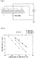
- the sheet sample 1 was sandwiched between the upper-arranged main electrode 2 and guard electrode 3 and the lower-arranged counter electrode 4, as shown in Fig. 1.
- a current value due to application of a voltage 500 V was measured at normal temperature and humidity by using an ammeter A.
- a resistance value ( ⁇ ) of the sample 1 was determined in compliance with Ohm's law.
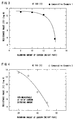
- the blending amount of N991 was changed as 70 weight part, 75 weight part and 80 weight part, in order to obtain resistance values. Results were obtained as shown in Table 1 and Figure 2.
- Samples with each carbon blending amount were prepared and measured similarly to Embodiment 1 excepting that the MT carbon of Embodiment 1 was changed to N908-UP (product name, produced by Cancarb) having a specific surface area - nitrogen absorption method of 9.5 m 2 /g, a dibutyl phthalate absorption number of 37 cm 3 /100g and mean particle size of 240 nm. Results were obtained as shown in table 1 and Figure 2.
- Samples with each carbon blending amount were prepared and measured similarly to Embodiment 1 excepting that the MT carbon of Embodiment 1 was changed to LPT (product name, produced by Cancarb) having a specific surface area - nitrogen absorption method of 8.5 m 2 /g, a dibutyl phthalate absorption number of 34 cm 3 /100g and an averaged particle size of 305 nm with the blending amount varied as 55 weight part, 60 weight part, 65 weight part and 70 weight part. Results were obtained as shown in Table 1 and Figure 2.
- LPT product name, produced by Cancarb
- samples with each carbon blending amount were prepared and measured similarly to Embodiment 1 excepting that the carbon black of Embodiment 1 was changed to Vulcan XC-72 (product name, produced by Cabot) having a specific surface area - nitrogen absorption method of 254 m 2 /g, a dibutyl phthalate absorption number of 174 cm 3 /100g and an averaged particle size of 30 nm. Results were obtained as shown in Table 2 and Figure 3. Resistance Value ( ⁇ ) Blending Amount of VULCAN XC-72 (Weight Part) 8 10 12 14 Comparative Example 1 1.0 ⁇ 10 13 7.0 ⁇ 10 12 1.7 ⁇ 10 12 4.7 ⁇ 10 5
- Samples with each carbon blending amount were prepared and measured similarly to Embodiment 1 excepting that the carbon black of Embodiment 1 was changed to Sevacarb MT-CI (product name, produced by Columbian Carbon) made by the oil furnace process and having a specific surface area - nitrogen absorption method of 8.0 m 2 /g, a dibutyl phthalate absorption number of 41 cm 3 /100g and an averaged particle size of 350 nm with the blending amount varied as 45 weight part, 50 weight part, 55 weight part and 60 weight part. Results were obtained as shown in Table 4 and Figure 5. Resistance Value (Q) Blending Amount of SEVACAB MT-CI (Weight Part) 45 50 55 60 Comparative Example 3 1.0 ⁇ 10 13 5.4 ⁇ 10 12 2.2 ⁇ 10 12 3.9 ⁇ 10 6
- Embodiments 1, 2 and 3 using MT carbon increased in carbon blending amount are free from abrupt lower in resistance value. If the MT carbon is increased by about 25 weight part with respect to 100 weight part of silicone rubber, the resistance value moderately lowers in a proportional fashion. In contrast, it was confirmed in each Comparative Example that there were regions where the resistance value is abruptly lowered by slight change in weight part (e.g. in Comparative Example 1, increase by 2 weight part from 12 to 14 weight part).
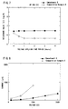
- a sample was prepared and measured similarly to Embodiment 4 except in that the N991 of Embodiment 4 was changed to 40 weight part of SRF-L#35 (product name, produced by Asahi Carbon) having a specific surface area - nitrogen absorption method of 24.0 m 2 /g, a dibutyl phthalate absorption number of 50 cm 3 /100g and an averaged particle size of 78 nm. Results were obtained as shown in Fig. 6.
- a sample was prepared similarly to Embodiment 1 excepting that N991 mentioned above was added in 45 weight part as silicone raw rubber to a 100 weight part of TSE201 (product name, produced by GE Toshiba Silicone).
- the current values on the sample were measured at normal temperature and humidity by using the ammeter while changing the application voltage from 0 to 2000 V.
- a resistance value R ( ⁇ ⁇ cm) of the sample when 500 V was applied was determined based on Ohm's law. Results are shown in Table 5 and Figure 8.
- a sample was prepared and measured similarly to Embodiment 6 excepting that the silicone raw rubber of Embodiment 6 was changed to TSE260-5U and the N991 was changed to 70 weight part of N908-UP. A result was obtained as shown in Table 5.
- a sample was prepared and measured similarly to Comparative Example 6 excepting that the carbon black of Comparative Example 6 was changed to 18 weight part of HAF#70 (product name, produced by Asahi Carbon) having a specific surface area - nitrogen absorption method of 77.0 m 2 /g, a dibutyl phthalate absorption number of 101 cm 3 /100g and an averaged particle size of 26 nm.
- HAF#70 product name, produced by Asahi Carbon
- Embodiments 6 to 10 using MT carbon have a resistance value held almost constant even if the application voltage is increased.
- a current value when applying 1000 V is I 1
- a current value when applying 2000 V is I 2
- the linear magnification expressed by I 2 /2I 1 is within a range of 1.2 to 1.5 and the dependency on voltage is extremely low.
- the resistance value greatly decreases with increase of application voltage.
- overcurrent flowed to make impossible to measure a current value I 2 Thus, a linear magnification could not be calculated.
Landscapes
- Chemical & Material Sciences (AREA)
- Health & Medical Sciences (AREA)
- Chemical Kinetics & Catalysis (AREA)
- Medicinal Chemistry (AREA)
- Polymers & Plastics (AREA)
- Organic Chemistry (AREA)
- Compositions Of Macromolecular Compounds (AREA)
- Pigments, Carbon Blacks, Or Wood Stains (AREA)
Abstract
Description
| Resistance Value (Ω) | ||||||
| Blending Amount of MT Carbon (Weight Part) | ||||||
| 55 | 60 | 65 | 70 | 75 | 80 | |
| Embodiment 1 | - | - | 1.8×10¹² | 1.6×10¹¹ | 1.8×10⁹ | 5.5×10⁷ |
| Embodiment 2 | - | - | 1.2×10¹¹ | 4.0×10⁹ | 1.3×10⁶ | 6.5×10⁴ |
| | 1.1×10¹³ | 1.1×10¹¹ | 7.4×10⁸ | 4.4×10⁶ | - | - |
| Resistance Value (Ω) | ||||
| Blending Amount of VULCAN XC-72 (Weight Part) | ||||
| 8 | 10 | 12 | 14 | |
| Comparative Example 1 | 1.0 × 10¹³ | 7.0 × 10¹² | 1.7 × 10¹² | 4.7 × 10⁵ |
| Resistance Value (Ω) | ||||
| Blending Amount of ASAHI THERMAL (Weight Part) | ||||
| 30 | 35 | 40 | 45 | |
| Comparative Example 2 | 1.6 × 10¹¹ | 2.3 × 10¹² | 8.2 × 10⁷ | 1.1 × 10⁵ |
| Resistance Value (Q) | ||||
| Blending Amount of SEVACAB MT-CI (Weight Part) | ||||
| 45 | 50 | 55 | 60 | |
| Comparative Example 3 | 1.0 × 10¹³ | 5.4 × 10¹² | 2.2 × 10¹² | 3.9 × 10⁶ |
| Voltage 500 (V) | Voltage 1000 (V) | Voltage 2000 (V) | Linearity Magnification (Times) | ||
| Volume Resistance Value RV (Ω · cm) | Current Value I (µA) | Current Value I1 (µA) | Current Value I2 (µA) | | |
| | 1.1 × 10¹⁰ | 48 | 135 | 380 | 1.4 |
| Embodiment 7 | 9.1 × 10⁸ | 417 | 824 | 1988 | 1.2 |
| | 7.6 × 10⁹ | 205 | 542 | 1352 | 1.5 |
| | 5.2 × 10⁹ | 256 | 593 | 1557 | 1.3 |
| | 1.5 × 10¹⁰ | 53 | 133 | 382 | 1.4 |
| Comparative Example 6 | 6.5 × 10⁹ | 250 | 833 | Non-Measurable | - |
| Comparative Example 7 | 1.2 × 10⁹ | 368 | 1700 | Non-Measurable | - |
| Comparative Example 8 | 4.4 × 10⁹ | 280 | 1360 | Non-Measurable | - |
| Comparative Example 9 | 4.9 × 10⁹ | 278 | 1330 | Non-Measurable | - |
Claims (6)
- A semi-conductive silicone rubber composition containing carbon black, wherein said carbon black includes thermal black obtained by thermally cracking a natural gas and having a specific surface area - nitrogen absorption method of 8.0 to 10.0 m2/g, a dibutyl phthalate absorption number of 30 to 40 cm3/100g and an average particle size of 200 to 300 nm.
- A composition according to claim 1, wherein said thermal black has a specific surface area of 9.0 to 9.5 m2/g, a dibutyl phthalate absorption number of 34 to 40 cm3/100g and an average particle size of 240 to 310 nm.
- A composition of claim 1, wherein said thermal black has a specific surface area of 9.0 to 9.5 m2/g, a dibutyl phthalate absorption number of 34 to 40 cm3/100g and an average particle size of 240 to 320 nm.
- A composition according to claim 1, wherein said silicone rubber is heat cured rubber based on polyorganosiloxane.
- A rubber roll, comprising:a conductive core member; anda silicone rubber layer coated on an outer peripheral surface of said conductive core member, said silicone rubber layer comprising a semiconductive silicone rubber composition containing carbon black, said carbon black including thermal black as defined in any of claims 1 to 3.
- A composition according to claim 5, wherein silicone rubber is heat cured rubber based on polyorganosiloxane.
Applications Claiming Priority (6)
| Application Number | Priority Date | Filing Date | Title |
|---|---|---|---|
| JP26661099 | 1999-09-21 | ||
| JP26661099 | 1999-09-21 | ||
| JP2000032658A JP3638008B2 (en) | 2000-02-03 | 2000-02-03 | Semiconductive silicone rubber roll |
| JP2000032658 | 2000-02-03 | ||
| JP2000177142A JP3649383B2 (en) | 1999-09-21 | 2000-06-08 | Method for stabilizing resistance value of semiconductive silicone rubber composition |
| JP2000177142 | 2000-06-08 |
Publications (3)
| Publication Number | Publication Date |
|---|---|
| EP1088849A2 true EP1088849A2 (en) | 2001-04-04 |
| EP1088849A3 EP1088849A3 (en) | 2001-10-31 |
| EP1088849B1 EP1088849B1 (en) | 2007-01-24 |
Family
ID=27335482
Family Applications (1)
| Application Number | Title | Priority Date | Filing Date |
|---|---|---|---|
| EP20000120156 Expired - Lifetime EP1088849B1 (en) | 1999-09-21 | 2000-09-21 | Semi-conductive silicone rubber composition |
Country Status (3)
| Country | Link |
|---|---|
| US (1) | US6444323B1 (en) |
| EP (1) | EP1088849B1 (en) |
| DE (1) | DE60033101T2 (en) |
Cited By (6)
| Publication number | Priority date | Publication date | Assignee | Title |
|---|---|---|---|---|
| US7138090B2 (en) | 2003-04-11 | 2006-11-21 | Therm-O-Disc, Incorporated | Vapor sensor and materials therefor |
| US7645422B2 (en) | 2003-04-11 | 2010-01-12 | Therm-O-Disc, Incorporated | Vapor sensor and materials therefor |
| US7708947B2 (en) | 2005-11-01 | 2010-05-04 | Therm-O-Disc, Incorporated | Methods of minimizing temperature cross-sensitivity in vapor sensors and compositions therefor |
| US8012420B2 (en) | 2006-07-18 | 2011-09-06 | Therm-O-Disc, Incorporated | Robust low resistance vapor sensor materials |
| US8691390B2 (en) | 2007-11-20 | 2014-04-08 | Therm-O-Disc, Incorporated | Single-use flammable vapor sensor films |
| CN105001641A (en) * | 2015-07-01 | 2015-10-28 | 昆明理工大学 | Carbon black filled pressure-sensitive conductive silicone rubber composite material and preparation method thereof |
Families Citing this family (5)
| Publication number | Priority date | Publication date | Assignee | Title |
|---|---|---|---|---|
| KR100592928B1 (en) * | 2002-11-13 | 2006-06-23 | 스미토모 고무 고교 가부시키가이샤 | A conductive elastomer composition, a conductive member using the composition, and an image forming apparatus provided with the conductive member |
| WO2007149783A1 (en) * | 2006-06-20 | 2007-12-27 | Polyone Corporation | Thermally conductive polymer compounds containing zinc sulfide and thermal carbon black |
| US20080025876A1 (en) * | 2006-07-26 | 2008-01-31 | Ramamurthy Praveen C | Vapor sensor materials having polymer-grafted conductive particles |
| JP5236111B1 (en) | 2012-02-17 | 2013-07-17 | キヤノン株式会社 | Developing member, process cartridge, and electrophotographic image forming apparatus |
| US11434345B2 (en) | 2017-04-18 | 2022-09-06 | Shin-Etsu Chemical Co., Ltd. | High dielectric insulating silicone rubber composition and electric field relaxation layer |
Family Cites Families (6)
| Publication number | Priority date | Publication date | Assignee | Title |
|---|---|---|---|---|
| DE2816872A1 (en) | 1978-04-18 | 1979-10-31 | Wacker Chemie Gmbh | PROCESS FOR PRODUCING ELECTRICALLY CONDUCTIVE ORGANOPOLYSILOXANE ELASTOMERS |
| JP2894526B2 (en) * | 1992-02-28 | 1999-05-24 | 東レ・ダウコーニング・シリコーン 株式会社 | Conductive silicone rubber composition for rolls |
| JP3424485B2 (en) | 1997-03-07 | 2003-07-07 | 富士ゼロックス株式会社 | Semiconductive roll |
| US6013201A (en) * | 1997-05-23 | 2000-01-11 | Shin-Estu Chemical Co., Ltd. | Semiconductive silicone rubber compositions and semiconductive silicone rubber rolls |
| JP3503454B2 (en) * | 1997-12-24 | 2004-03-08 | 信越化学工業株式会社 | Semiconductive silicone rubber composition and semiconductive silicone rubber roll |
| JPH11106657A (en) * | 1997-09-30 | 1999-04-20 | Shin Etsu Polymer Co Ltd | Silicone rubber composition and conductive silicone rubber member using the same |
-
2000
- 2000-09-14 US US09/662,040 patent/US6444323B1/en not_active Expired - Fee Related
- 2000-09-21 DE DE2000633101 patent/DE60033101T2/en not_active Expired - Lifetime
- 2000-09-21 EP EP20000120156 patent/EP1088849B1/en not_active Expired - Lifetime
Cited By (9)
| Publication number | Priority date | Publication date | Assignee | Title |
|---|---|---|---|---|
| US7138090B2 (en) | 2003-04-11 | 2006-11-21 | Therm-O-Disc, Incorporated | Vapor sensor and materials therefor |
| AU2004201531B2 (en) * | 2003-04-11 | 2009-12-03 | Therm-O-Disc, Incorporated | Vapor sensor and materials therefor |
| US7645422B2 (en) | 2003-04-11 | 2010-01-12 | Therm-O-Disc, Incorporated | Vapor sensor and materials therefor |
| US7708947B2 (en) | 2005-11-01 | 2010-05-04 | Therm-O-Disc, Incorporated | Methods of minimizing temperature cross-sensitivity in vapor sensors and compositions therefor |
| US8012420B2 (en) | 2006-07-18 | 2011-09-06 | Therm-O-Disc, Incorporated | Robust low resistance vapor sensor materials |
| US8105538B2 (en) | 2006-07-18 | 2012-01-31 | Therm-O-Disc Incorporated | Robust low resistance vapor sensor materials |
| AU2007201456B2 (en) * | 2006-08-28 | 2013-03-07 | Therm-O-Disc Incorporated | Vapor sensor and materials therefor |
| US8691390B2 (en) | 2007-11-20 | 2014-04-08 | Therm-O-Disc, Incorporated | Single-use flammable vapor sensor films |
| CN105001641A (en) * | 2015-07-01 | 2015-10-28 | 昆明理工大学 | Carbon black filled pressure-sensitive conductive silicone rubber composite material and preparation method thereof |
Also Published As
| Publication number | Publication date |
|---|---|
| EP1088849B1 (en) | 2007-01-24 |
| DE60033101T2 (en) | 2007-11-08 |
| EP1088849A3 (en) | 2001-10-31 |
| US6444323B1 (en) | 2002-09-03 |
| DE60033101D1 (en) | 2007-03-15 |
Similar Documents
| Publication | Publication Date | Title |
|---|---|---|
| US6444323B1 (en) | Semi-conductive silicone rubber composition | |
| EP0609038B1 (en) | Semiconductor rolls | |
| US5725922A (en) | Semiconductive silicone rubber compositions and semiconductive silicone rubber rolls | |
| EP2652043B1 (en) | Methods to control electrical resistivity in filler-polymer compositions and products related thereto | |
| JPH08339904A (en) | Positive temperature coefficient composition | |
| JP3501055B2 (en) | Semiconductive silicone rubber composition and silicone rubber roll | |
| US6013201A (en) | Semiconductive silicone rubber compositions and semiconductive silicone rubber rolls | |
| JP4196779B2 (en) | Process for producing conductive composition for electrophotographic equipment | |
| JP3649383B2 (en) | Method for stabilizing resistance value of semiconductive silicone rubber composition | |
| US6648807B2 (en) | Conductive rubber roller | |
| JP3638008B2 (en) | Semiconductive silicone rubber roll | |
| JP2005220317A (en) | Conductive composition for electrophotographic equipment, process for producing the same, and electroconductive member for electrophotographic equipment using the same | |
| KR20190068433A (en) | Conductive silicone composition and silicone composite prepared thereby | |
| JP3158879B2 (en) | Semiconductive silicone rubber members for office machines | |
| JPH0816195B2 (en) | Method for producing rubber composition | |
| JPH07258548A (en) | Conductive silicone rubber composition | |
| JP3383536B2 (en) | Semiconductive silicone rubber composition and silicone rubber roll | |
| JPH06166819A (en) | Method for producing conductive silicone rubber composition | |
| JP3503454B2 (en) | Semiconductive silicone rubber composition and semiconductive silicone rubber roll | |
| JP3656904B2 (en) | Conductive rubber roller | |
| JP2885651B2 (en) | Semiconductive rubber composition | |
| JPH1135830A (en) | Semiconductive silicone rubber composition and semiconductive silicone rubber roll | |
| JP3166026B2 (en) | Semiconductive silicone rubber composition and silicone rubber roll | |
| JP5514452B2 (en) | Conductive resin composition and molded body thereof | |
| JP3748133B2 (en) | Rubber composition |
Legal Events
| Date | Code | Title | Description |
|---|---|---|---|
| PUAI | Public reference made under article 153(3) epc to a published international application that has entered the european phase |
Free format text: ORIGINAL CODE: 0009012 |
|
| AK | Designated contracting states |
Kind code of ref document: A2 Designated state(s): AT BE CH CY DE DK ES FI FR GB GR IE IT LI LU MC NL PT SE Kind code of ref document: A2 Designated state(s): DE FR GB IT |
|
| AX | Request for extension of the european patent |
Free format text: AL;LT;LV;MK;RO;SI |
|
| PUAL | Search report despatched |
Free format text: ORIGINAL CODE: 0009013 |
|
| AK | Designated contracting states |
Kind code of ref document: A3 Designated state(s): AT BE CH CY DE DK ES FI FR GB GR IE IT LI LU MC NL PT SE |
|
| AX | Request for extension of the european patent |
Free format text: AL;LT;LV;MK;RO;SI |
|
| 17P | Request for examination filed |
Effective date: 20020311 |
|
| AKX | Designation fees paid |
Free format text: DE FR GB IT |
|
| 17Q | First examination report despatched |
Effective date: 20030123 |
|
| GRAP | Despatch of communication of intention to grant a patent |
Free format text: ORIGINAL CODE: EPIDOSNIGR1 |
|
| GRAS | Grant fee paid |
Free format text: ORIGINAL CODE: EPIDOSNIGR3 |
|
| GRAA | (expected) grant |
Free format text: ORIGINAL CODE: 0009210 |
|
| AK | Designated contracting states |
Kind code of ref document: B1 Designated state(s): DE FR GB IT |
|
| REG | Reference to a national code |
Ref country code: GB Ref legal event code: FG4D |
|
| REF | Corresponds to: |
Ref document number: 60033101 Country of ref document: DE Date of ref document: 20070315 Kind code of ref document: P |
|
| EN | Fr: translation not filed | ||
| PLBE | No opposition filed within time limit |
Free format text: ORIGINAL CODE: 0009261 |
|
| STAA | Information on the status of an ep patent application or granted ep patent |
Free format text: STATUS: NO OPPOSITION FILED WITHIN TIME LIMIT |
|
| 26N | No opposition filed |
Effective date: 20071025 |
|
| PG25 | Lapsed in a contracting state [announced via postgrant information from national office to epo] |
Ref country code: FR Free format text: LAPSE BECAUSE OF FAILURE TO SUBMIT A TRANSLATION OF THE DESCRIPTION OR TO PAY THE FEE WITHIN THE PRESCRIBED TIME-LIMIT Effective date: 20070914 Ref country code: IT Free format text: LAPSE BECAUSE OF FAILURE TO SUBMIT A TRANSLATION OF THE DESCRIPTION OR TO PAY THE FEE WITHIN THE PRESCRIBED TIME-LIMIT Effective date: 20070124 |
|
| PG25 | Lapsed in a contracting state [announced via postgrant information from national office to epo] |
Ref country code: FR Free format text: LAPSE BECAUSE OF FAILURE TO SUBMIT A TRANSLATION OF THE DESCRIPTION OR TO PAY THE FEE WITHIN THE PRESCRIBED TIME-LIMIT Effective date: 20070124 |
|
| PGFP | Annual fee paid to national office [announced via postgrant information from national office to epo] |
Ref country code: GB Payment date: 20090916 Year of fee payment: 10 |
|
| PGFP | Annual fee paid to national office [announced via postgrant information from national office to epo] |
Ref country code: DE Payment date: 20090923 Year of fee payment: 10 |
|
| GBPC | Gb: european patent ceased through non-payment of renewal fee |
Effective date: 20100921 |
|
| REG | Reference to a national code |
Ref country code: DE Ref legal event code: R119 Ref document number: 60033101 Country of ref document: DE Effective date: 20110401 |
|
| PG25 | Lapsed in a contracting state [announced via postgrant information from national office to epo] |
Ref country code: DE Free format text: LAPSE BECAUSE OF NON-PAYMENT OF DUE FEES Effective date: 20110401 |
|
| PG25 | Lapsed in a contracting state [announced via postgrant information from national office to epo] |
Ref country code: GB Free format text: LAPSE BECAUSE OF NON-PAYMENT OF DUE FEES Effective date: 20100921 |