EP1087648A2 - Multi-purpose finish for printed wiring boards and method of manufacture of such boards - Google Patents
Multi-purpose finish for printed wiring boards and method of manufacture of such boards Download PDFInfo
- Publication number
- EP1087648A2 EP1087648A2 EP00307856A EP00307856A EP1087648A2 EP 1087648 A2 EP1087648 A2 EP 1087648A2 EP 00307856 A EP00307856 A EP 00307856A EP 00307856 A EP00307856 A EP 00307856A EP 1087648 A2 EP1087648 A2 EP 1087648A2
- Authority
- EP
- European Patent Office
- Prior art keywords
- recited
- palladium
- pwb
- alloy
- cobalt
- Prior art date
- Legal status (The legal status is an assumption and is not a legal conclusion. Google has not performed a legal analysis and makes no representation as to the accuracy of the status listed.)
- Granted
Links
Images


Classifications
-
- H—ELECTRICITY
- H05—ELECTRIC TECHNIQUES NOT OTHERWISE PROVIDED FOR
- H05K—PRINTED CIRCUITS; CASINGS OR CONSTRUCTIONAL DETAILS OF ELECTRIC APPARATUS; MANUFACTURE OF ASSEMBLAGES OF ELECTRICAL COMPONENTS
- H05K3/00—Apparatus or processes for manufacturing printed circuits
- H05K3/22—Secondary treatment of printed circuits
- H05K3/24—Reinforcing of the conductive pattern
- H05K3/244—Finish plating of conductors, especially of copper conductors, e.g. for pads or lands
-
- H—ELECTRICITY
- H05—ELECTRIC TECHNIQUES NOT OTHERWISE PROVIDED FOR
- H05K—PRINTED CIRCUITS; CASINGS OR CONSTRUCTIONAL DETAILS OF ELECTRIC APPARATUS; MANUFACTURE OF ASSEMBLAGES OF ELECTRICAL COMPONENTS
- H05K3/00—Apparatus or processes for manufacturing printed circuits
- H05K3/22—Secondary treatment of printed circuits
-
- H—ELECTRICITY
- H05—ELECTRIC TECHNIQUES NOT OTHERWISE PROVIDED FOR
- H05K—PRINTED CIRCUITS; CASINGS OR CONSTRUCTIONAL DETAILS OF ELECTRIC APPARATUS; MANUFACTURE OF ASSEMBLAGES OF ELECTRICAL COMPONENTS
- H05K3/00—Apparatus or processes for manufacturing printed circuits
- H05K3/02—Apparatus or processes for manufacturing printed circuits in which the conductive material is applied to the surface of the insulating support and is thereafter removed from such areas of the surface which are not intended for current conducting or shielding
- H05K3/06—Apparatus or processes for manufacturing printed circuits in which the conductive material is applied to the surface of the insulating support and is thereafter removed from such areas of the surface which are not intended for current conducting or shielding the conductive material being removed chemically or electrolytically, e.g. by photo-etch process
- H05K3/061—Etching masks
- H05K3/062—Etching masks consisting of metals or alloys or metallic inorganic compounds
-
- H—ELECTRICITY
- H05—ELECTRIC TECHNIQUES NOT OTHERWISE PROVIDED FOR
- H05K—PRINTED CIRCUITS; CASINGS OR CONSTRUCTIONAL DETAILS OF ELECTRIC APPARATUS; MANUFACTURE OF ASSEMBLAGES OF ELECTRICAL COMPONENTS
- H05K2203/00—Indexing scheme relating to apparatus or processes for manufacturing printed circuits covered by H05K3/00
- H05K2203/05—Patterning and lithography; Masks; Details of resist
- H05K2203/0562—Details of resist
- H05K2203/0571—Dual purpose resist, e.g. etch resist used as solder resist, solder resist used as plating resist
-
- H—ELECTRICITY
- H05—ELECTRIC TECHNIQUES NOT OTHERWISE PROVIDED FOR
- H05K—PRINTED CIRCUITS; CASINGS OR CONSTRUCTIONAL DETAILS OF ELECTRIC APPARATUS; MANUFACTURE OF ASSEMBLAGES OF ELECTRICAL COMPONENTS
- H05K3/00—Apparatus or processes for manufacturing printed circuits
- H05K3/10—Apparatus or processes for manufacturing printed circuits in which conductive material is applied to the insulating support in such a manner as to form the desired conductive pattern
- H05K3/108—Apparatus or processes for manufacturing printed circuits in which conductive material is applied to the insulating support in such a manner as to form the desired conductive pattern by semi-additive methods; masks therefor
-
- H—ELECTRICITY
- H05—ELECTRIC TECHNIQUES NOT OTHERWISE PROVIDED FOR
- H05K—PRINTED CIRCUITS; CASINGS OR CONSTRUCTIONAL DETAILS OF ELECTRIC APPARATUS; MANUFACTURE OF ASSEMBLAGES OF ELECTRICAL COMPONENTS
- H05K3/00—Apparatus or processes for manufacturing printed circuits
- H05K3/22—Secondary treatment of printed circuits
- H05K3/28—Applying non-metallic protective coatings
-
- H—ELECTRICITY
- H05—ELECTRIC TECHNIQUES NOT OTHERWISE PROVIDED FOR
- H05K—PRINTED CIRCUITS; CASINGS OR CONSTRUCTIONAL DETAILS OF ELECTRIC APPARATUS; MANUFACTURE OF ASSEMBLAGES OF ELECTRICAL COMPONENTS
- H05K3/00—Apparatus or processes for manufacturing printed circuits
- H05K3/38—Improvement of the adhesion between the insulating substrate and the metal
- H05K3/382—Improvement of the adhesion between the insulating substrate and the metal by special treatment of the metal
- H05K3/384—Improvement of the adhesion between the insulating substrate and the metal by special treatment of the metal by plating
-
- H—ELECTRICITY
- H10—SEMICONDUCTOR DEVICES; ELECTRIC SOLID-STATE DEVICES NOT OTHERWISE PROVIDED FOR
- H10W—GENERIC PACKAGES, INTERCONNECTIONS, CONNECTORS OR OTHER CONSTRUCTIONAL DETAILS OF DEVICES COVERED BY CLASS H10
- H10W72/00—Interconnections or connectors in packages
- H10W72/071—Connecting or disconnecting
- H10W72/072—Connecting or disconnecting of bump connectors
-
- H—ELECTRICITY
- H10—SEMICONDUCTOR DEVICES; ELECTRIC SOLID-STATE DEVICES NOT OTHERWISE PROVIDED FOR
- H10W—GENERIC PACKAGES, INTERCONNECTIONS, CONNECTORS OR OTHER CONSTRUCTIONAL DETAILS OF DEVICES COVERED BY CLASS H10
- H10W72/00—Interconnections or connectors in packages
- H10W72/071—Connecting or disconnecting
- H10W72/075—Connecting or disconnecting of bond wires
-
- H—ELECTRICITY
- H10—SEMICONDUCTOR DEVICES; ELECTRIC SOLID-STATE DEVICES NOT OTHERWISE PROVIDED FOR
- H10W—GENERIC PACKAGES, INTERCONNECTIONS, CONNECTORS OR OTHER CONSTRUCTIONAL DETAILS OF DEVICES COVERED BY CLASS H10
- H10W72/00—Interconnections or connectors in packages
- H10W72/90—Bond pads, in general
- H10W72/951—Materials of bond pads
- H10W72/952—Materials of bond pads comprising metals or metalloids, e.g. PbSn, Ag or Cu
-
- Y—GENERAL TAGGING OF NEW TECHNOLOGICAL DEVELOPMENTS; GENERAL TAGGING OF CROSS-SECTIONAL TECHNOLOGIES SPANNING OVER SEVERAL SECTIONS OF THE IPC; TECHNICAL SUBJECTS COVERED BY FORMER USPC CROSS-REFERENCE ART COLLECTIONS [XRACs] AND DIGESTS
- Y10—TECHNICAL SUBJECTS COVERED BY FORMER USPC
- Y10T—TECHNICAL SUBJECTS COVERED BY FORMER US CLASSIFICATION
- Y10T29/00—Metal working
- Y10T29/49—Method of mechanical manufacture
- Y10T29/49002—Electrical device making
- Y10T29/49117—Conductor or circuit manufacturing
- Y10T29/49124—On flat or curved insulated base, e.g., printed circuit, etc.
- Y10T29/4913—Assembling to base an electrical component, e.g., capacitor, etc.
- Y10T29/49144—Assembling to base an electrical component, e.g., capacitor, etc. by metal fusion
-
- Y—GENERAL TAGGING OF NEW TECHNOLOGICAL DEVELOPMENTS; GENERAL TAGGING OF CROSS-SECTIONAL TECHNOLOGIES SPANNING OVER SEVERAL SECTIONS OF THE IPC; TECHNICAL SUBJECTS COVERED BY FORMER USPC CROSS-REFERENCE ART COLLECTIONS [XRACs] AND DIGESTS
- Y10—TECHNICAL SUBJECTS COVERED BY FORMER USPC
- Y10T—TECHNICAL SUBJECTS COVERED BY FORMER US CLASSIFICATION
- Y10T29/00—Metal working
- Y10T29/49—Method of mechanical manufacture
- Y10T29/49002—Electrical device making
- Y10T29/49117—Conductor or circuit manufacturing
- Y10T29/49124—On flat or curved insulated base, e.g., printed circuit, etc.
- Y10T29/49147—Assembling terminal to base
- Y10T29/49149—Assembling terminal to base by metal fusion bonding
-
- Y—GENERAL TAGGING OF NEW TECHNOLOGICAL DEVELOPMENTS; GENERAL TAGGING OF CROSS-SECTIONAL TECHNOLOGIES SPANNING OVER SEVERAL SECTIONS OF THE IPC; TECHNICAL SUBJECTS COVERED BY FORMER USPC CROSS-REFERENCE ART COLLECTIONS [XRACs] AND DIGESTS
- Y10—TECHNICAL SUBJECTS COVERED BY FORMER USPC
- Y10T—TECHNICAL SUBJECTS COVERED BY FORMER US CLASSIFICATION
- Y10T29/00—Metal working
- Y10T29/49—Method of mechanical manufacture
- Y10T29/49002—Electrical device making
- Y10T29/49117—Conductor or circuit manufacturing
- Y10T29/49124—On flat or curved insulated base, e.g., printed circuit, etc.
- Y10T29/49155—Manufacturing circuit on or in base
-
- Y—GENERAL TAGGING OF NEW TECHNOLOGICAL DEVELOPMENTS; GENERAL TAGGING OF CROSS-SECTIONAL TECHNOLOGIES SPANNING OVER SEVERAL SECTIONS OF THE IPC; TECHNICAL SUBJECTS COVERED BY FORMER USPC CROSS-REFERENCE ART COLLECTIONS [XRACs] AND DIGESTS
- Y10—TECHNICAL SUBJECTS COVERED BY FORMER USPC
- Y10T—TECHNICAL SUBJECTS COVERED BY FORMER US CLASSIFICATION
- Y10T428/00—Stock material or miscellaneous articles
- Y10T428/12—All metal or with adjacent metals
- Y10T428/12493—Composite; i.e., plural, adjacent, spatially distinct metal components [e.g., layers, joint, etc.]
- Y10T428/12528—Semiconductor component
-
- Y—GENERAL TAGGING OF NEW TECHNOLOGICAL DEVELOPMENTS; GENERAL TAGGING OF CROSS-SECTIONAL TECHNOLOGIES SPANNING OVER SEVERAL SECTIONS OF THE IPC; TECHNICAL SUBJECTS COVERED BY FORMER USPC CROSS-REFERENCE ART COLLECTIONS [XRACs] AND DIGESTS
- Y10—TECHNICAL SUBJECTS COVERED BY FORMER USPC
- Y10T—TECHNICAL SUBJECTS COVERED BY FORMER US CLASSIFICATION
- Y10T428/00—Stock material or miscellaneous articles
- Y10T428/12—All metal or with adjacent metals
- Y10T428/12493—Composite; i.e., plural, adjacent, spatially distinct metal components [e.g., layers, joint, etc.]
- Y10T428/12736—Al-base component
- Y10T428/1275—Next to Group VIII or IB metal-base component
-
- Y—GENERAL TAGGING OF NEW TECHNOLOGICAL DEVELOPMENTS; GENERAL TAGGING OF CROSS-SECTIONAL TECHNOLOGIES SPANNING OVER SEVERAL SECTIONS OF THE IPC; TECHNICAL SUBJECTS COVERED BY FORMER USPC CROSS-REFERENCE ART COLLECTIONS [XRACs] AND DIGESTS
- Y10—TECHNICAL SUBJECTS COVERED BY FORMER USPC
- Y10T—TECHNICAL SUBJECTS COVERED BY FORMER US CLASSIFICATION
- Y10T428/00—Stock material or miscellaneous articles
- Y10T428/12—All metal or with adjacent metals
- Y10T428/12493—Composite; i.e., plural, adjacent, spatially distinct metal components [e.g., layers, joint, etc.]
- Y10T428/12771—Transition metal-base component
- Y10T428/12861—Group VIII or IB metal-base component
- Y10T428/12875—Platinum group metal-base component
-
- Y—GENERAL TAGGING OF NEW TECHNOLOGICAL DEVELOPMENTS; GENERAL TAGGING OF CROSS-SECTIONAL TECHNOLOGIES SPANNING OVER SEVERAL SECTIONS OF THE IPC; TECHNICAL SUBJECTS COVERED BY FORMER USPC CROSS-REFERENCE ART COLLECTIONS [XRACs] AND DIGESTS
- Y10—TECHNICAL SUBJECTS COVERED BY FORMER USPC
- Y10T—TECHNICAL SUBJECTS COVERED BY FORMER US CLASSIFICATION
- Y10T428/00—Stock material or miscellaneous articles
- Y10T428/12—All metal or with adjacent metals
- Y10T428/12493—Composite; i.e., plural, adjacent, spatially distinct metal components [e.g., layers, joint, etc.]
- Y10T428/12771—Transition metal-base component
- Y10T428/12861—Group VIII or IB metal-base component
- Y10T428/12882—Cu-base component alternative to Ag-, Au-, or Ni-base component
-
- Y—GENERAL TAGGING OF NEW TECHNOLOGICAL DEVELOPMENTS; GENERAL TAGGING OF CROSS-SECTIONAL TECHNOLOGIES SPANNING OVER SEVERAL SECTIONS OF THE IPC; TECHNICAL SUBJECTS COVERED BY FORMER USPC CROSS-REFERENCE ART COLLECTIONS [XRACs] AND DIGESTS
- Y10—TECHNICAL SUBJECTS COVERED BY FORMER USPC
- Y10T—TECHNICAL SUBJECTS COVERED BY FORMER US CLASSIFICATION
- Y10T428/00—Stock material or miscellaneous articles
- Y10T428/12—All metal or with adjacent metals
- Y10T428/12493—Composite; i.e., plural, adjacent, spatially distinct metal components [e.g., layers, joint, etc.]
- Y10T428/12771—Transition metal-base component
- Y10T428/12861—Group VIII or IB metal-base component
- Y10T428/12903—Cu-base component
- Y10T428/1291—Next to Co-, Cu-, or Ni-base component
Definitions
- the present invention is directed, in general, to circuit boards and, more specifically, to a multi-purpose finish for printed wiring boards (PWBs) and method of manufacture of such PWBs.
- PWBs printed wiring boards
- PWB Printed Wiring Board
- Manufacturing processes are changing at a rapid rate because of the increasing demand for enhanced performance.
- the demand for enhanced performance is due to higher circuit densities, an increase in board complexities and an increase in the cost of environmental compliance.
- Many types of final finishes are used on PWBs. Final finish selection is generally dependent on the requirements the board must ultimately meet.
- Surface circuits on PWBs usually include copper and copper alloy materials that should be coated to provide good mechanical and electrical connection with other devices in the assembly.
- the coating on the circuits is called the surface finish.
- the circuits include non-contact areas and contact areas.
- the finish applied to the non-contact areas is called non-contact finish and the finish applied to the contact areas is called contact finish.
- the non-contact areas include wirebonding areas, chip attach areas, soldering areas and other non-contact areas. Both non-contact and contact finishes must meet certain different requirements. Non-contact finish requirements include good solderability, good wirebonding performance (for some PWBs, depending on applications), and high corrosion resistance. Contact finish requirements on the other hand, include high conductivity, high wear resistance and high corrosion resistance. To meet these different requirements, different coatings have been used for non-contact finishes and contact finishes.
- Some typical non-contact finishes include hot air solder level (HASL) coating, electroless nickel coating with immersion gold on top (EN/IAu), organic solderability preservative (OSP) coating, and organo-metallic, such as organo-silver, solderability preservative (OSP/Ag).
- a typical contact finish may include an electrolytic nickel coating with an electrolytic hard gold layer (gold-nickel or gold-cobalt alloys with nickel or cobalt less than 0.3 wt.%) on top.
- HASL The most common non-contact finish process in circuit boards is HASL.
- the use of HASL over the last few years has decreased dramatically. This is primarily due to the increasing demand for boards employable in mixed technologies, including surface mount technologies, of which HASL is not.
- a photoresist layer is placed on a base copper laminate substrate, and subjected to ultraviolet light, which develops the pattern for the desired circuits.
- the photoresist is washed, leaving openings in the areas that were masked off from the UV light, in the pattern of the circuits on the copper laminate.
- Electrolytic copper (acid copper) is then plated on top of the base copper laminate on the circuit areas, through the openings in the photoresist.
- a layer of tin or tin-lead is pattern plated on the circuits to act as an etch resist.
- the remaining photoresist material is stripped from the substrate, exposing the base copper laminate.
- the base copper laminate is then removed, exposing the bare substrate (commonly glass enforced plastics). At this point in the HASL process, nothing remains on the substrate except the etch resist material plated on the copper circuit lines.
- etch resist material has to first be applied and then removed, and usually solder mask (SM) applied before HASL finishing can be accomplished.
- SM solder mask
- HASL coatings cannot be employed in the applications of mixed technologies due to their inability to meet substrate coplanarity and wire bonding requirements.
- the HASL finishing is a labor and maintenance intensive process and causes many environmental concerns because it usually contains lead.
- OSP and OSP/Ag are two of these post etch technologies applied directly to the surface of copper circuits. However, they have limited storage lives, degrade when exposed to soldering temperature and do not have good wire bondability.
- a contact finish such as an electrolytic nickel layer with an electrolytic hard gold on top, must be applied on the contact areas after the non-contact finish is coated (as suggested previously).
- the contact finish has good conductivity and high wear resistance. However, it cannot be used as a non-contact finish due to its poor solderability and wire bondability. And to apply the contact finish to the board requires another masking step where SM is applied, the contact finish plated, then the SM stripped off. This increases processing steps and decreases production yields due to mis-registration of the SM.
- palladium or palladium-nickel alloys might be used as a multi-purpose finish in PWBs.
- pure palladium suffers from relatively high porosity and relatively high cost, and palladium-nickel alloys exhibit lower wear resistance than what is needed for today's demanding technologies.
- the present invention provides a multi-purpose finish for a PWB and a method of manufacturing the same.
- the PWB includes: (1) a substrate having a conductive trace located thereon and (2) a multi-purpose finish including palladium alloy where palladium is alloyed with cobalt or a platinum group metal and is located on at least a portion of the conductive trace, which forms both a non-contact finish and a contact finish for the PWB.
- Platinum group metal is a metal selected from the group consisting of Ruthenium, Rhodium, Palladium, Rhenium, Osmium, Iridium and Platinum.
- the PWB may also preferably include a material formed over the multi-purpose finish, and in such instances, the material may be palladium, silver, gold, rhodium, ruthenium, platinum, tin or their alloys, or an organic solderability preservative (OSP).
- OSP organic solderability preservative
- nickel may be applied, using conventional deposition processes, under the palladium alloy, forming a nickel under-layer.
- the nickel deposition step may be optional and omitted in some applications.
- other materials such as nickel alloy, cobalt, cobalt alloy, iron or iron alloy may also be used.
- the non-contact areas comprise surface-mount pads, wire bond pads, solder pads or interconnections.
- Interconnections as used by Applicants are defined as the circuit traces, plated through holes (PTH) and micro-vias.
- PTH plated through holes
- the palladium alloy may be advantageously employed in other PWB finishes, such as for vias or decorative designs.
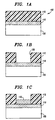
- FIGURE 1A there is illustrated a PWB 103 having a substrate 105, normally a material, such as glass enforced plastic, on which numerous layers may be formed. While the substrate 105 illustrated in this advantageous embodiment is composed of glass enforced plastic, those skilled in the art will realize that the substrate 105 may be composed of any substrate materials, including epoxies, polyimides, fluorinated polymers, ceramics, polyesters, phenolics, and aramide paper.
- a base copper laminate 110 or similar laminate material is placed over the entire substrate 105. Following the application of the base copper laminate 110, a photoresist layer 115 is then applied on top of the base copper laminate 110. The photoresist layer 115 is subjected to ultraviolet light which exposes the circuit trace pattern thereon and the circuit trace pattern is formed as seen in FIGURE 1B.
- an electrolytic copper plate 122 is formed in the opening 120 created by the photoresist, and on top of the base copper laminate 110.
- other types of copper, or similar material may also be used.
- a nickel layer 124 nickel under-layer
- the nickel layer 124 is placed upon the electrolytic copper plate 122 to prevent oxidation of the copper and to give additional hardness to the surface finish.
- Nickel like copper, is known to oxidize and produce nickel oxide, but contrary to copper oxide, nickel oxide does not creep along the surface.
- Nickel's tendency to produce nickel oxide is further reduced when the palladium alloy, is applied over nickel. While nickel is described in this embodiment, those skilled in the art should understand that the nickel deposition step may be optional and omitted in some applications. However, where nickel is required it should also be understood that materials similar to nickel such as nickel alloys, cobalt, cobalt alloys, iron and iron alloys may be used.
- a layer of a palladium alloy 125 is placed over the nickel layer 124, which is on top of the electrolytic copper plate 122.
- the palladium alloy 125 replaces the tin or tin-lead plating process present in conventional processes.
- the palladium is alloyed with cobalt or a platinum group metal as defined herein.
- the alloy may further include a tertiary metal, such as nickel or iron.
- the cobalt comprises about 1 wt.% or more of the palladium-cobalt alloy.
- the palladium alloy 125 illustrated may be comprised of 80 wt.% palladium and 20 wt.% cobalt or platinum group metal.
- the palladium alloy 125 may be comprised of palladium ranging from about 50 to about 95 wt.% of the alloy and cobalt or a platinum group metal ranging from about 5 to about 50 wt.% percent of the alloy.
- Other details of how the palladium alloy 125 may be formed are described in detail in U.S. Patent No. 5,976,344.
- the palladium alloy 125 provides in PWB manufacturing is its use as an etch resist replacement for tin or tin-lead.
- the palladium alloy 125 may now be used as a multi-purpose finish for both non-contact and contact finishes.
- the use of a palladium alloy 125 not only removes lead from the surface finishing production area, a major waste treatment expense, but the cycle time becomes much shorter as the plating and subsequent stripping of the etch resist material is eliminated. Fabrication time is substantially shortened because about 50% of the processing steps can be eliminated.
- the palladium alloys 125 have a characteristic of low porosity. Low porosity minimizes formation of corrosion products of exposed copper and/or nickel on the surface of the palladium alloy, which in turn, preserves conductivity, solderability and wire bondability of the surface.
- the palladium alloy 125 provides superior wear resistance, excellent diffusion/migration barrier properties, high thermal stability and good coplanarity. All these properties make the palladium alloy 125 a good finish for both non-contact and contact areas.
- the photoresist layer 115 is stripped. This uncovers portions of the base copper laminate 110 that are to be removed.
- the exposed base copper laminate 110 which was formerly covered by the photoresist (see FIGURE 1E), is etched away using conventional copper etch processes, which results in the circuit traces 130 as illustrated in FIGURE 1F.
- the palladium alloy 125 acts as an etch resist to a portion of the copper circuit traces 130. What is left after the resist strip and copper etch is a substrate 105, covered by a copper circuitry 130.
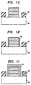
- the final, required, step of the process is shown in FIGURE 1G, and comprises the function of applying a solder mask 135 to the substrate 105.
- a solder mask 135 is applied to prevent solder bridges from forming during the assembly performed by the board user.
- the exposed copper circuitry 130 may be covered with a protective coating, in an additional step.
- the protective coating may be a variety of coatings, such as palladium, silver, gold, rhodium, ruthenium, platinum, tin or their alloys, or organic solderability preservative (OSP). These coatings may be applied by conventional processes.
- FIGURES 1H through 1J illustrate three of the many processes that may be applied to prevent copper creep.
- the copper circuitry 130 can be subjected to an immersion palladium plate 140 after the solder mask 135 is applied to the substrate 105. (See FIGURE 1H).
- the immersion palladium plate 140 is applied in a manner similar to electroless plating except that the reduction of metal ions in the plating solution is accomplished by the oxidation of the metal on the part being plated, rather than by a reducing agent in the solution.
- an electroless palladium plate 145 can be applied.
- the electroless palladium plate 145 is formed using a reduction process and covers the remaining copper circuitry 130.
- Using an electroless palladium plate provides more even thickness distribution, than when using an electrolytic palladium plate and greater thickness than received when using an immersion palladium plate 140.
- FIGURE 1J Another process, as shown in FIGURE 1J, consists of subjecting the PWB apparatus in FIGURE 1G to an immersion gold plate 150.
- an immersion gold plate 150 over the copper circuitry 130, an increase in solderability, wire bondability and wear resistance is achieved.
- Gold increases the wetting speed of the product when subjected to the molten solder, which in turn increases the solderability of the surface.
- the commonality of the two materials makes for a stronger wire bond.
- the properties of gold help it to function as a form of lubrication, which in turn increases the wear resistance of the surface.
- FIGURE 2 is a flow chart showing the various steps that might occur in the embodiments just discussed above.
- one embodiment may further include a clean copper laminate/substrate step 205 followed by a micro-etch copper laminate/substrate step 210 and an acid dip copper laminate/substrate step 215.
- the copper and the substrate may also be acid dipped in step 225.
- the substrate may undergo a pre-clean step 245.
- the other steps appearing in FIGURE 2 have been discussed with respect to the previously described embodiments.
Landscapes
- Engineering & Computer Science (AREA)
- Manufacturing & Machinery (AREA)
- Microelectronics & Electronic Packaging (AREA)
- Metallurgy (AREA)
- Manufacturing Of Printed Wiring (AREA)
- Electroplating Methods And Accessories (AREA)
- Parts Printed On Printed Circuit Boards (AREA)
- Manufacturing Of Printed Circuit Boards (AREA)
Abstract
Description
- The present invention is directed, in general, to circuit boards and, more specifically, to a multi-purpose finish for printed wiring boards (PWBs) and method of manufacture of such PWBs.
- Printed Wiring Board (PWB) manufacturing processes are changing at a rapid rate because of the increasing demand for enhanced performance. The demand for enhanced performance is due to higher circuit densities, an increase in board complexities and an increase in the cost of environmental compliance. Many types of final finishes are used on PWBs. Final finish selection is generally dependent on the requirements the board must ultimately meet. Surface circuits on PWBs usually include copper and copper alloy materials that should be coated to provide good mechanical and electrical connection with other devices in the assembly.
- Typically, the coating on the circuits is called the surface finish. The circuits include non-contact areas and contact areas. The finish applied to the non-contact areas is called non-contact finish and the finish applied to the contact areas is called contact finish. The non-contact areas include wirebonding areas, chip attach areas, soldering areas and other non-contact areas. Both non-contact and contact finishes must meet certain different requirements. Non-contact finish requirements include good solderability, good wirebonding performance (for some PWBs, depending on applications), and high corrosion resistance. Contact finish requirements on the other hand, include high conductivity, high wear resistance and high corrosion resistance. To meet these different requirements, different coatings have been used for non-contact finishes and contact finishes.
- Some typical non-contact finishes include hot air solder level (HASL) coating, electroless nickel coating with immersion gold on top (EN/IAu), organic solderability preservative (OSP) coating, and organo-metallic, such as organo-silver, solderability preservative (OSP/Ag). A typical contact finish may include an electrolytic nickel coating with an electrolytic hard gold layer (gold-nickel or gold-cobalt alloys with nickel or cobalt less than 0.3 wt.%) on top. To coat any of the above non-contact finishes on the circuits and to coat the finish on the contact areas requires considerable processing steps (24-28 steps), and a great amount of time, all of which decreases production yields and increases cost.
- The most common non-contact finish process in circuit boards is HASL. The use of HASL over the last few years has decreased dramatically. This is primarily due to the increasing demand for boards employable in mixed technologies, including surface mount technologies, of which HASL is not. In manufacturing a PWB using HASL, a photoresist layer is placed on a base copper laminate substrate, and subjected to ultraviolet light, which develops the pattern for the desired circuits. Next, the photoresist is washed, leaving openings in the areas that were masked off from the UV light, in the pattern of the circuits on the copper laminate. Electrolytic copper (acid copper) is then plated on top of the base copper laminate on the circuit areas, through the openings in the photoresist. After applying the electrolytic copper, a layer of tin or tin-lead, is pattern plated on the circuits to act as an etch resist. The remaining photoresist material is stripped from the substrate, exposing the base copper laminate. The base copper laminate is then removed, exposing the bare substrate (commonly glass enforced plastics). At this point in the HASL process, nothing remains on the substrate except the etch resist material plated on the copper circuit lines.
- One disadvantage of this process is that extra-processing steps have to be applied. The etch resist material has to first be applied and then removed, and usually solder mask (SM) applied before HASL finishing can be accomplished. Furthermore, HASL coatings cannot be employed in the applications of mixed technologies due to their inability to meet substrate coplanarity and wire bonding requirements. The HASL finishing is a labor and maintenance intensive process and causes many environmental concerns because it usually contains lead.
- The EN/IAu process requires essentially the same steps, up through the removal of tin or tin-lead and applying of SM, as the HASL process. Then, instead of applying flux and undergoing HASL, plating of electroless nickel and immersion gold is performed on the circuits. As with the HASL process, the EN/Au process has also many disadvantages. It suffers from high porosity, many processing steps, degradation when exposed to soldering temperatures and high expense.
- There are many other competing technologies that are applied, but all require an etch resist to first be applied and then removed, demanding many processing steps. OSP and OSP/Ag are two of these post etch technologies applied directly to the surface of copper circuits. However, they have limited storage lives, degrade when exposed to soldering temperature and do not have good wire bondability.
- None of the above-mentioned non-contact finishes can be used as a contact finish due to their poor wear resistence.
- A contact finish, such as an electrolytic nickel layer with an electrolytic hard gold on top, must be applied on the contact areas after the non-contact finish is coated (as suggested previously). The contact finish has good conductivity and high wear resistance. However, it cannot be used as a non-contact finish due to its poor solderability and wire bondability. And to apply the contact finish to the board requires another masking step where SM is applied, the contact finish plated, then the SM stripped off. This increases processing steps and decreases production yields due to mis-registration of the SM.
- The PWB industry has recently started to evaluate alternative surface finishes. There is a high demand for a multi-purpose finish that can be used for both non-contact circuits and contact areas and that can replace tin-lead in the PWB finishing process, to lower environmental concerns and make electronic circuit manufacturing "greener." To be qualified, such a finish should provide high etch resistance, good solderability, good wirebonding performance, high conductivity, high wear resistance, high corrosion resistance/low porosity, coplanarity (uniform thickness distribution), integrity after exposure to soldering temperatures for up to 10 minutes, ability to integrate into present manufacturing stream, long storage life (6 to 12 months), favorable economics and environmental safety. With such a finish, one can dramatically reduce the processing steps, increase the production throughput, reduce the cost and improve the quality of the PWBs. It was previously thought that palladium or palladium-nickel alloys might be used as a multi-purpose finish in PWBs. However, pure palladium suffers from relatively high porosity and relatively high cost, and palladium-nickel alloys exhibit lower wear resistance than what is needed for today's demanding technologies.
- Accordingly, what is needed in the art is a multi-purpose finish that meets all the above-mentioned requirements and achieves all the above-mentioned objectives.
- To address the above-discussed deficiencies of the prior art, the present invention provides a multi-purpose finish for a PWB and a method of manufacturing the same. In one embodiment, the PWB includes: (1) a substrate having a conductive trace located thereon and (2) a multi-purpose finish including palladium alloy where palladium is alloyed with cobalt or a platinum group metal and is located on at least a portion of the conductive trace, which forms both a non-contact finish and a contact finish for the PWB. Platinum group metal is a metal selected from the group consisting of Ruthenium, Rhodium, Palladium, Rhenium, Osmium, Iridium and Platinum.
- The present invention therefore introduces the broad concept of employing a palladium alloy, where the palladium alloy is alloyed with cobalt or a platinum group metal, as a multi-purpose finish for PWBs, suitable for forming both non-contact and contact finishes. The palladium alloy when alloyed with cobalt includes about 1 wt.% or more of cobalt and may further include nickel or iron. The palladium alloy may further be alloyed with both cobalt and a platinum group metal. The palladium alloy acts also as an etch resist layer.
- In one embodiment, the non-contact finish coats at least a portion of a non-contact area. In a related embodiment, the contact finish coats at least a portion of a contact area. In another embodiment the palladium alloy is located on all of the conductive traces. The conductive traces preferably comprise copper. However, other conductive materials such as copper alloys, aluminum, nickel, silver, gold, platinum or their alloys may be used for the conductive traces.
- The palladium alloy employed in the present invention is such that palladium comprises a weight percent of the palladium alloy ranging from about 10 wt.% to about 95 wt.% and cobalt or a platinum group metal comprises a weight percent of the palladium alloy ranging from about 5 wt.% to about 90 wt.% of the palladium alloy.
- The PWB may also preferably include a material formed over the multi-purpose finish, and in such instances, the material may be palladium, silver, gold, rhodium, ruthenium, platinum, tin or their alloys, or an organic solderability preservative (OSP).
- In another embodiment, nickel may be applied, using conventional deposition processes, under the palladium alloy, forming a nickel under-layer. Those skilled in the art should understand that the nickel deposition step may be optional and omitted in some applications. However, where nickel is required it should also be understood that other materials such as nickel alloy, cobalt, cobalt alloy, iron or iron alloy may also be used.
- In another embodiment of the present invention, the non-contact areas comprise surface-mount pads, wire bond pads, solder pads or interconnections. Interconnections as used by Applicants are defined as the circuit traces, plated through holes (PTH) and micro-vias. Those skilled in the pertinent art will realize, however, that the palladium alloy may be advantageously employed in other PWB finishes, such as for vias or decorative designs.
- The substrate may comprise various materials that are typically used for PWB fabrication. Examples of these materials contain epoxies, polyimides, fluorinated polymers, ceramics, polyesters, phenolics, and aramide paper.
- The foregoing has outlined, rather broadly, preferred and alternative features of the present invention so that those skilled in the art may better understand the detailed description of the invention that follows. Additional features of the invention are described hereinafter that form the subject of the claims of the invention. Those skilled in the art should appreciate that they can readily use the disclosed conception and specific embodiment as a basis for designing other structures for carrying out the same purposes of the present invention. Those skilled in the art should also realize that such equivalent constructions do not depart from the spirit and scope of the invention in its broadest form.
- For a more complete understanding of the present invention, reference is now made to the following descriptions taken in conjunction with the accompanying drawings, in which:
- FIGUREs 1A through 1J illustrate exemplary, cross-sectional views of a printed wiring board (PWB), which are not drawn to scale, constructed according to the principles of the present invention; and
- FIGURE 2 illustrates a method for using a palladium alloy as a final finish for a PWB.
-
- Turning initially to FIGURE 1A there is illustrated a
PWB 103 having asubstrate 105, normally a material, such as glass enforced plastic, on which numerous layers may be formed. While thesubstrate 105 illustrated in this advantageous embodiment is composed of glass enforced plastic, those skilled in the art will realize that thesubstrate 105 may be composed of any substrate materials, including epoxies, polyimides, fluorinated polymers, ceramics, polyesters, phenolics, and aramide paper. Abase copper laminate 110 or similar laminate material is placed over theentire substrate 105. Following the application of thebase copper laminate 110, aphotoresist layer 115 is then applied on top of thebase copper laminate 110. Thephotoresist layer 115 is subjected to ultraviolet light which exposes the circuit trace pattern thereon and the circuit trace pattern is formed as seen in FIGURE 1B. - Using an acid copper plating method, an
electrolytic copper plate 122 is formed in theopening 120 created by the photoresist, and on top of thebase copper laminate 110. However, other types of copper, or similar material, may also be used. (see FIGURE 1C). Next, as shown in FIGURE 1D, a nickel layer 124 (nickel under-layer) is plated within theopening 120, and on top of theelectrolytic copper plate 122, by conventional deposition processes. Thenickel layer 124 is placed upon theelectrolytic copper plate 122 to prevent oxidation of the copper and to give additional hardness to the surface finish. Nickel, like copper, is known to oxidize and produce nickel oxide, but contrary to copper oxide, nickel oxide does not creep along the surface. Nickel's tendency to produce nickel oxide is further reduced when the palladium alloy, is applied over nickel. While nickel is described in this embodiment, those skilled in the art should understand that the nickel deposition step may be optional and omitted in some applications. However, where nickel is required it should also be understood that materials similar to nickel such as nickel alloys, cobalt, cobalt alloys, iron and iron alloys may be used. - Referring next to FIGURE 1E, a layer of a
palladium alloy 125 is placed over thenickel layer 124, which is on top of theelectrolytic copper plate 122. Thepalladium alloy 125 replaces the tin or tin-lead plating process present in conventional processes. The palladium is alloyed with cobalt or a platinum group metal as defined herein. In those embodiments where the palladium is alloyed with cobalt, the alloy may further include a tertiary metal, such as nickel or iron. In these particular embodiments, the cobalt comprises about 1 wt.% or more of the palladium-cobalt alloy. In another embodiment, thepalladium alloy 125 illustrated may be comprised of 80 wt.% palladium and 20 wt.% cobalt or platinum group metal. However, those skilled in the art will realize, of course, that similar ratios of palladium to cobalt or a platinum group metal may also be used. For example, it has been found that thepalladium alloy 125 may be comprised of palladium ranging from about 50 to about 95 wt.% of the alloy and cobalt or a platinum group metal ranging from about 5 to about 50 wt.% percent of the alloy. Other details of how thepalladium alloy 125 may be formed are described in detail in U.S. Patent No. 5,976,344. - Other details regarding electroplating palladium alloys are described in U.S. Patent Application, Serial No. 08/644,347, filed May 10, 1996, which is also incorporated herein by reference.
- One major advantage that the
palladium alloy 125 provides in PWB manufacturing is its use as an etch resist replacement for tin or tin-lead. When used in this manner, thepalladium alloy 125 may now be used as a multi-purpose finish for both non-contact and contact finishes. The use of apalladium alloy 125 not only removes lead from the surface finishing production area, a major waste treatment expense, but the cycle time becomes much shorter as the plating and subsequent stripping of the etch resist material is eliminated. Fabrication time is substantially shortened because about 50% of the processing steps can be eliminated. - The
palladium alloys 125, as defined herein, have a characteristic of low porosity. Low porosity minimizes formation of corrosion products of exposed copper and/or nickel on the surface of the palladium alloy, which in turn, preserves conductivity, solderability and wire bondability of the surface. - Likewise, the
palladium alloy 125 provides superior wear resistance, excellent diffusion/migration barrier properties, high thermal stability and good coplanarity. All these properties make the palladium alloy 125 a good finish for both non-contact and contact areas. - After the
palladium alloy 125 deposition, thephotoresist layer 115 is stripped. This uncovers portions of thebase copper laminate 110 that are to be removed. The exposedbase copper laminate 110, which was formerly covered by the photoresist (see FIGURE 1E), is etched away using conventional copper etch processes, which results in the circuit traces 130 as illustrated in FIGURE 1F. Thepalladium alloy 125 acts as an etch resist to a portion of the copper circuit traces 130. What is left after the resist strip and copper etch is asubstrate 105, covered by acopper circuitry 130. - The final, required, step of the process is shown in FIGURE 1G, and comprises the function of applying a
solder mask 135 to thesubstrate 105. Asolder mask 135 is applied to prevent solder bridges from forming during the assembly performed by the board user. - One concern is that after using the
palladium alloy 125 as an etch resist, there may be exposedcopper circuitry 130 on the circuit side walls. The exposedcopper circuitry 130 may be covered with a protective coating, in an additional step. The protective coating may be a variety of coatings, such as palladium, silver, gold, rhodium, ruthenium, platinum, tin or their alloys, or organic solderability preservative (OSP). These coatings may be applied by conventional processes. - FIGURES 1H through 1J illustrate three of the many processes that may be applied to prevent copper creep. In one optional step, the
copper circuitry 130 can be subjected to animmersion palladium plate 140 after thesolder mask 135 is applied to thesubstrate 105. (See FIGURE 1H). Theimmersion palladium plate 140 is applied in a manner similar to electroless plating except that the reduction of metal ions in the plating solution is accomplished by the oxidation of the metal on the part being plated, rather than by a reducing agent in the solution. - As shown in FIGURE 1I, which is an alternative to an
immersion palladium plate 140, anelectroless palladium plate 145 can be applied. Theelectroless palladium plate 145 is formed using a reduction process and covers the remainingcopper circuitry 130. Using an electroless palladium plate provides more even thickness distribution, than when using an electrolytic palladium plate and greater thickness than received when using animmersion palladium plate 140. - Another process, as shown in FIGURE 1J, consists of subjecting the PWB apparatus in FIGURE 1G to an
immersion gold plate 150. By using animmersion gold plate 150 over thecopper circuitry 130, an increase in solderability, wire bondability and wear resistance is achieved. Gold increases the wetting speed of the product when subjected to the molten solder, which in turn increases the solderability of the surface. Additionally, since most wires that are attached to the surface of a PWB comprise gold and the surface comprises gold, the commonality of the two materials makes for a stronger wire bond. Also, the properties of gold help it to function as a form of lubrication, which in turn increases the wear resistance of the surface. - FIGURE 2 is a flow chart showing the various steps that might occur in the embodiments just discussed above. As shown, one embodiment may further include a clean copper laminate/
substrate step 205 followed by a micro-etch copper laminate/substrate step 210 and an acid dip copper laminate/substrate step 215. Following the copper plating, the copper and the substrate may also be acid dipped instep 225. To assure a clean surface on which to form the solder mask, the substrate may undergo apre-clean step 245. The other steps appearing in FIGURE 2 have been discussed with respect to the previously described embodiments. - As a result of the discussions above, the use of a palladium alloy as a multi-purpose PWB finish on both non-contact circuits and contact areas reduces more than 50% of the process steps, maintains or even improves the required material properties, and achieves considerable cost saving. Cost saving is achieved through process step reduction, cheaper deposit material, and improved finish performance.
- Although the present invention has been described in detail, those skilled in the art should understand that they can make various changes, substitutions and alterations herein without departing from the scope of the invention as set out in the claims.
Claims (33)
- A printed wiring board (PWB), comprising:a substrate having a conductive trace thereon; anda multi-purpose finish including palladium alloy, wherein palladium is alloyed with cobalt or a platinum group metal, said palladium alloy located on at least portions of said conductive trace, that forms both a non-contact finish and a contact finish for said PWB.
- The PWB as recited in Claim 1 wherein said palladium alloy is palladium-cobalt alloy and said palladium-cobalt alloy further includes nickel or iron.
- The PWB as recited in Claim 2 wherein said cobalt comprises about 1 wt.% or more of said palladium-cobalt alloy.
- The PWB as recited in Claim 1 wherein said palladium alloy is an etch resist layer.
- The PWB as recited in Claim 1 wherein said non-contact finish coats at least a portion of a non-contact area.
- The PWB as recited in Claim 1 wherein said contact finish coats at least a portion of a contact area.
- The PWB as recited in Claim 1 wherein said conductive trace is comprised of a metal selected from the group consisting of:copper;copper alloys;aluminum;aluminum alloys;nickel;nickel alloys;silver;gold; andplatinum.
- The PWB as recited in Claim 1 wherein palladium comprises a weight percent of said palladium alloy ranging from about 10 wt.% to about 95 wt.% and cobalt or a platinum group metal comprises a weight percent of said palladium alloy ranging from about 5 wt.% to about 90 wt.% of said palladium alloy.
- The PWB as recited in Claim 1 wherein palladium comprises a weight percent of said palladium alloy ranging from about 50 wt.% to about 95 wt.% and cobalt or a platinum group metal comprises a weight percent of said palladium alloy ranging from about 5 wt.% to about 50 wt.% of said palladium alloy.
- The PWB as recited in Claim 1 further comprising a material formed over said multi-purpose finish wherein said material is selected from the group consisting of:palladium;silver;gold;rhodium;ruthenium;platinum;tin; andorganic solderability preservative (OSP).
- The PWB as recited in Claim 1 wherein an under-layer located under said palladium alloy comprises a material selected from the group consisting of:nickel;nickel alloys;cobalt;cobalt alloys;iron; andiron alloys.
- The PWB as recited in Claim 1 wherein said palladium alloy is located on all of said conductive traces.
- The PWB as recited in Claim 5 wherein said non-contact area is selected from the group consisting of:a surface-mount pad,a wire bond pad,a solder pad, andan interconnection.
- The PWB as recited in Claim 1 wherein said substrate is comprised of a material selected from the group consisting of:epoxies;polyimides;fluorinated polymers;ceramics;polyesters;phenolics; andaramide paper.
- A method of manufacturing a printed wiring board (PWB), comprising:forming conductive traces on a substrate;depositing a multi-purpose finish including palladium alloy, wherein palladium is alloyed with cobalt or a platinum group metal, on predetermined portions of said conductive traces; andsubjecting said PWB to an etching process, a portion of said multi-purpose finish remaining to form both a non-contact finish and a contact finish for said PWB.
- The method as recited in Claim 15 wherein said palladium alloy is palladium-cobalt alloy and said palladium-cobalt alloy further includes nickel or iron.
- The method as recited in Claim 16 wherein said cobalt comprises about 1 wt.% or more of said palladium-cobalt alloy.
- The method as recited in Claim 15 wherein said palladium alloy is an etch resist layer.
- The method as recited in Claim 15 wherein said non-contact finish coats at least a portion of a non-contact area.
- The method as recited in Claim 15 wherein said contact finish coats at least a portion of a contact area.
- The method as recited in Claim 15 wherein said forming comprises acid copper plating said conductive traces.
- The method as recited in Claim 15 wherein said depositing comprises plating said multi-purpose finish.
- The method as recited in Claim 19 further comprising surface mounting components to said non-contact area.
- The method as recited in Claim 19 further comprising wire bonding electrical components to said non-contact area.
- The method as recited in Claim 19 further comprising forming solder pads on said non-contact area.
- The method as recited in Claim 19 further comprising forming interconnections in said non-contact area.
- The method as recited in Claim 15 wherein said conductive traces are comprised of a metal selected from the group consisting of:copper;copper alloys;aluminum;aluminum alloys;nickel;nickel alloys;silver;gold; andplatinum.
- The method as recited in Claim 15 wherein palladium comprises a weight percent of said palladium alloy ranging from about 10 wt.% to about 95 wt.% and cobalt or a platinum group metal comprises a weight percent of said palladium alloy ranging from about 5 wt.% to about 90 wt.% of said palladium alloy.
- The method as recited in Claim 15 wherein palladium comprises a weight percent of said palladium alloy ranging from about 50 wt.% to about 95 wt.% and cobalt or a platinum group metal comprises a weight percent of said palladium alloy ranging from about 5 wt.% to about 50 wt.% of said palladium alloy.
- The method as recited in Claim 15 further comprising, forming a material over said multi-purpose finish, said material selected from the group consisting of:palladium;silver;gold;rhodium;ruthenium;platinum;tin; andorganic solderability preservative (OSP).
- The method as recited in Claim 15 further including forming an under-layer on said conductive trace, selected from the group consisting of:nickel;nickel alloy;cobalt;cobalt alloy;iron; and iron alloy.
- The method as recited in Claim 19 wherein said non-contact area is selected from the group consisting of:a surface-mount pad,a wire bond pad,a solder pad, andan interconnection.
- The method as recited in Claim 15 wherein said substrate is comprised of material selected from the group consisting of:epoxies;polyimides;fluorinated polymers;ceramics;polyesters;phenolics; andaramide paper.
Applications Claiming Priority (2)
| Application Number | Priority Date | Filing Date | Title |
|---|---|---|---|
| US09/405,368 US6534192B1 (en) | 1999-09-24 | 1999-09-24 | Multi-purpose finish for printed wiring boards and method of manufacture of such boards |
| US405368 | 1999-09-24 |
Publications (3)
| Publication Number | Publication Date |
|---|---|
| EP1087648A2 true EP1087648A2 (en) | 2001-03-28 |
| EP1087648A3 EP1087648A3 (en) | 2005-09-07 |
| EP1087648B1 EP1087648B1 (en) | 2009-07-08 |
Family
ID=23603418
Family Applications (1)
| Application Number | Title | Priority Date | Filing Date |
|---|---|---|---|
| EP00307856A Expired - Lifetime EP1087648B1 (en) | 1999-09-24 | 2000-09-11 | Multi-purpose finish for printed wiring boards and method of manufacture of such boards |
Country Status (5)
| Country | Link |
|---|---|
| US (2) | US6534192B1 (en) |
| EP (1) | EP1087648B1 (en) |
| JP (1) | JP3662825B2 (en) |
| KR (1) | KR100356322B1 (en) |
| DE (1) | DE60042514D1 (en) |
Cited By (9)
| Publication number | Priority date | Publication date | Assignee | Title |
|---|---|---|---|---|
| US7622377B2 (en) | 2005-09-01 | 2009-11-24 | Micron Technology, Inc. | Microfeature workpiece substrates having through-substrate vias, and associated methods of formation |
| WO2012118896A3 (en) * | 2011-03-03 | 2013-01-17 | Skyworks Solutions, Inc. | Apparatus and methods related to wire bond pads and reducing impact of high rf loss plating |
| US8686537B2 (en) | 2011-03-03 | 2014-04-01 | Skyworks Solutions, Inc. | Apparatus and methods for reducing impact of high RF loss plating |
| US8889995B2 (en) | 2011-03-03 | 2014-11-18 | Skyworks Solutions, Inc. | Wire bond pad system and method |
| CN104981092A (en) * | 2015-06-17 | 2015-10-14 | 三星半导体(中国)研究开发有限公司 | Surface plating and semiconductor package including the surface plating |
| WO2016154315A1 (en) | 2015-03-23 | 2016-09-29 | Texas Instruments Incorporated | Metal bond pad with cobalt interconnect layer and solder thereon |
| US9660584B2 (en) | 2012-06-14 | 2017-05-23 | Skyworks Solutions, Inc. | Power amplifier modules including wire bond pad and related systems, devices, and methods |
| US10049970B2 (en) | 2015-06-17 | 2018-08-14 | Samsung Electronics Co., Ltd. | Methods of manufacturing printed circuit board and semiconductor package |
| US11984423B2 (en) | 2011-09-02 | 2024-05-14 | Skyworks Solutions, Inc. | Radio frequency transmission line with finish plating on conductive layer |
Families Citing this family (61)
| Publication number | Priority date | Publication date | Assignee | Title |
|---|---|---|---|---|
| KR100396787B1 (en) * | 2001-11-13 | 2003-09-02 | 엘지전자 주식회사 | Wire bonding pad structure of semiconductor package pcb |
| KR100476409B1 (en) * | 2002-06-07 | 2005-03-16 | 엘지전자 주식회사 | Plating method for PCB |
| US6984358B2 (en) * | 2002-09-13 | 2006-01-10 | Lockheed Martin Corporation | Diffusion bonding process of two-phase metal alloys |
| US7091124B2 (en) | 2003-11-13 | 2006-08-15 | Micron Technology, Inc. | Methods for forming vias in microelectronic devices, and methods for packaging microelectronic devices |
| US8084866B2 (en) | 2003-12-10 | 2011-12-27 | Micron Technology, Inc. | Microelectronic devices and methods for filling vias in microelectronic devices |
| US20050247894A1 (en) | 2004-05-05 | 2005-11-10 | Watkins Charles M | Systems and methods for forming apertures in microfeature workpieces |
| TWI256280B (en) * | 2004-06-10 | 2006-06-01 | Geetmann Taiwan Ltd | Method of raising manufacturing-yield of circuit board |
| US7232754B2 (en) | 2004-06-29 | 2007-06-19 | Micron Technology, Inc. | Microelectronic devices and methods for forming interconnects in microelectronic devices |
| JP2006080493A (en) * | 2004-08-12 | 2006-03-23 | Ricoh Microelectronics Co Ltd | Electrode substrate |
| SG120200A1 (en) | 2004-08-27 | 2006-03-28 | Micron Technology Inc | Slanted vias for electrical circuits on circuit boards and other substrates |
| JP4815771B2 (en) * | 2004-09-01 | 2011-11-16 | 住友電気工業株式会社 | Manufacturing method of electrical parts |
| US7300857B2 (en) | 2004-09-02 | 2007-11-27 | Micron Technology, Inc. | Through-wafer interconnects for photoimager and memory wafers |
| KR100601493B1 (en) * | 2004-12-30 | 2006-07-18 | 삼성전기주식회사 | BA package having a half-etched bonding pad and a cut plating line and manufacturing method thereof |
| US7271482B2 (en) | 2004-12-30 | 2007-09-18 | Micron Technology, Inc. | Methods for forming interconnects in microelectronic workpieces and microelectronic workpieces formed using such methods |
| US7795134B2 (en) * | 2005-06-28 | 2010-09-14 | Micron Technology, Inc. | Conductive interconnect structures and formation methods using supercritical fluids |
| US7863187B2 (en) | 2005-09-01 | 2011-01-04 | Micron Technology, Inc. | Microfeature workpieces and methods for forming interconnects in microfeature workpieces |
| US7262134B2 (en) | 2005-09-01 | 2007-08-28 | Micron Technology, Inc. | Microfeature workpieces and methods for forming interconnects in microfeature workpieces |
| US20080173470A1 (en) * | 2005-10-03 | 2008-07-24 | Michael Barbetta | Combined Solderable Multi-Purpose Surface Finishes on Circuit Boards and Method of Manufacture of Such Boards |
| US20070221503A1 (en) * | 2006-03-22 | 2007-09-27 | Brian Larson | Precoat composition for organic solderability preservative |
| US7749899B2 (en) | 2006-06-01 | 2010-07-06 | Micron Technology, Inc. | Microelectronic workpieces and methods and systems for forming interconnects in microelectronic workpieces |
| US7629249B2 (en) | 2006-08-28 | 2009-12-08 | Micron Technology, Inc. | Microfeature workpieces having conductive interconnect structures formed by chemically reactive processes, and associated systems and methods |
| US7972710B2 (en) | 2006-08-31 | 2011-07-05 | Antaya Technologies Corporation | Clad aluminum connector |
| US7902643B2 (en) | 2006-08-31 | 2011-03-08 | Micron Technology, Inc. | Microfeature workpieces having interconnects and conductive backplanes, and associated systems and methods |
| US20080268267A1 (en) * | 2007-04-27 | 2008-10-30 | Michael Barbetta | Combined solderable multi-purpose surface finishes on circuit boards and method of manufacture of such boards |
| SG150410A1 (en) | 2007-08-31 | 2009-03-30 | Micron Technology Inc | Partitioned through-layer via and associated systems and methods |
| US8641855B2 (en) * | 2007-09-25 | 2014-02-04 | Siemens Energy, Inc. | Method for spacing electrical conductors and related devices |
| JP4706690B2 (en) * | 2007-11-05 | 2011-06-22 | パナソニック電工株式会社 | Circuit board and manufacturing method thereof |
| US7884015B2 (en) | 2007-12-06 | 2011-02-08 | Micron Technology, Inc. | Methods for forming interconnects in microelectronic workpieces and microelectronic workpieces formed using such methods |
| US8594627B2 (en) * | 2008-10-06 | 2013-11-26 | Telecommunications Systems, Inc. | Remotely provisioned wirelessly proxy |
| EP2216796A1 (en) * | 2009-02-05 | 2010-08-11 | Delphi Technologies, Inc. | Sliding contact assembly |
| US8263177B2 (en) * | 2009-03-27 | 2012-09-11 | Kesheng Feng | Organic polymer coating for protection against creep corrosion |
| DE102009038674B4 (en) * | 2009-08-24 | 2012-02-09 | Epcos Ag | Carrier device, arrangement with such a carrier device and method for producing a structured layer stack comprising at least one ceramic layer |
| US8834729B2 (en) * | 2009-11-30 | 2014-09-16 | Eastman Kodak Company | Method of making bondable printed wiring member |
| JP5232823B2 (en) * | 2010-03-30 | 2013-07-10 | Jx日鉱日石金属株式会社 | Copper foil for printed wiring board excellent in etching property and laminate using the same |
| KR101184796B1 (en) * | 2010-12-29 | 2012-09-20 | 와이엠티 주식회사 | board structure and method for manufacturing the same |
| US8801914B2 (en) * | 2011-05-26 | 2014-08-12 | Eastman Kodak Company | Method of making wear-resistant printed wiring member |
| KR102014088B1 (en) * | 2012-03-20 | 2019-08-26 | 엘지이노텍 주식회사 | Memory card, pcb for the memory card and method for manufacturing the same |
| JP6075606B2 (en) * | 2012-09-26 | 2017-02-08 | 京セラ株式会社 | Wiring board and electronic device |
| JP2014187204A (en) * | 2013-03-22 | 2014-10-02 | Toshiba Corp | Semiconductor device manufacturing method and semiconductor device |
| CN103984009B (en) * | 2014-04-16 | 2016-04-13 | 刘致水 | Based on three kinds of porosity type quantitative inversion methods of P-wave And S well-log information |
| JP6311200B2 (en) * | 2014-06-26 | 2018-04-18 | 住友電工プリントサーキット株式会社 | Printed wiring board, electronic component, and printed wiring board manufacturing method |
| CN205726641U (en) * | 2016-01-04 | 2016-11-23 | 奥特斯(中国)有限公司 | There is the parts carrier of different surface layer and the electronic equipment containing this parts carrier |
| US10937915B2 (en) | 2016-10-28 | 2021-03-02 | Tesla, Inc. | Obscuring, color matching, and camouflaging solar panels |
| US12598838B2 (en) | 2016-11-09 | 2026-04-07 | Tesla, Inc. | System and methods for achieving a micro louver effect in a photovoltaic cell |
| CN108738240A (en) * | 2017-04-19 | 2018-11-02 | 鹏鼎控股(深圳)股份有限公司 | Flexible PCB and preparation method thereof |
| US10381973B2 (en) | 2017-05-17 | 2019-08-13 | Tesla, Inc. | Uniformly and directionally colored photovoltaic modules |
| US10985688B2 (en) | 2017-06-05 | 2021-04-20 | Tesla, Inc. | Sidelap interconnect for photovoltaic roofing modules |
| US10734938B2 (en) | 2017-07-21 | 2020-08-04 | Tesla, Inc. | Packaging for solar roof tiles |
| US10857764B2 (en) | 2017-07-25 | 2020-12-08 | Tesla, Inc. | Method for improving adhesion between glass cover and encapsulant for solar roof tiles |
| US10978990B2 (en) | 2017-09-28 | 2021-04-13 | Tesla, Inc. | Glass cover with optical-filtering coating for managing color of a solar roof tile |
| US10454409B2 (en) | 2018-02-02 | 2019-10-22 | Tesla, Inc. | Non-flat solar roof tiles |
| US10862420B2 (en) | 2018-02-20 | 2020-12-08 | Tesla, Inc. | Inter-tile support for solar roof tiles |
| US11190128B2 (en) | 2018-02-27 | 2021-11-30 | Tesla, Inc. | Parallel-connected solar roof tile modules |
| CA3268022A1 (en) | 2018-03-01 | 2025-10-30 | Tesla, Inc. | System and method for packaging photovoltaic roof tiles |
| US11431279B2 (en) | 2018-07-02 | 2022-08-30 | Tesla, Inc. | Solar roof tile with a uniform appearance |
| US11082005B2 (en) | 2018-07-31 | 2021-08-03 | Tesla, Inc. | External electrical contact for solar roof tiles |
| US11245354B2 (en) | 2018-07-31 | 2022-02-08 | Tesla, Inc. | Solar roof tile spacer with embedded circuitry |
| US11245355B2 (en) | 2018-09-04 | 2022-02-08 | Tesla, Inc. | Solar roof tile module |
| US11581843B2 (en) | 2018-09-14 | 2023-02-14 | Tesla, Inc. | Solar roof tile free of back encapsulant layer |
| US11431280B2 (en) | 2019-08-06 | 2022-08-30 | Tesla, Inc. | System and method for improving color appearance of solar roofs |
| US20230122858A1 (en) * | 2021-10-14 | 2023-04-20 | Compass Technology Company Limited | Method of Embedding a Multi-Layer Lithium Ion Battery on a Flexible Printed Circuit Board |
Citations (2)
| Publication number | Priority date | Publication date | Assignee | Title |
|---|---|---|---|---|
| US4911798A (en) | 1988-12-20 | 1990-03-27 | At&T Bell Laboratories | Palladium alloy plating process |
| DE4201129A1 (en) | 1991-01-18 | 1992-07-23 | Ishihara Chemical Co Ltd | Palladium-coated printed wiring boards - for integrated circuits, with improved solderability |
Family Cites Families (13)
| Publication number | Priority date | Publication date | Assignee | Title |
|---|---|---|---|---|
| EP0083488A3 (en) * | 1981-12-31 | 1985-11-06 | O'Hara, James Brian | Method of producing printed circuits |
| GB2137421A (en) * | 1983-03-15 | 1984-10-03 | Standard Telephones Cables Ltd | Printed circuits |
| US4529667A (en) * | 1983-04-06 | 1985-07-16 | The Furukawa Electric Company, Ltd. | Silver-coated electric composite materials |
| US4872851A (en) * | 1989-02-27 | 1989-10-10 | International Business Machines Corp. | Electrical connector with torsional contacts |
| KR0171685B1 (en) * | 1994-02-26 | 1999-02-18 | 문성수 | Palladium binary or ternary alloy plating composition, plating method and plating body using the same |
| DE4431847C5 (en) * | 1994-09-07 | 2011-01-27 | Atotech Deutschland Gmbh | Substrate with bondable coating |
| US5674326A (en) * | 1994-09-21 | 1997-10-07 | Motorola, Inc. | Solder paste |
| US5608966A (en) * | 1994-12-14 | 1997-03-11 | International Business Machines Corporation | Process for manufacture of spring contact elements and assembly thereof |
| JPH09232493A (en) * | 1995-12-20 | 1997-09-05 | Seiichi Serizawa | Lead frame |
| US5976344A (en) * | 1996-05-10 | 1999-11-02 | Lucent Technologies Inc. | Composition for electroplating palladium alloys and electroplating process using that composition |
| JPH1046384A (en) * | 1996-05-10 | 1998-02-17 | Lucent Technol Inc | Palladium alloy plating bath |
| US6162365A (en) * | 1998-03-04 | 2000-12-19 | International Business Machines Corporation | Pd etch mask for copper circuitization |
| US6180523B1 (en) * | 1998-10-13 | 2001-01-30 | Industrial Technology Research Institute | Copper metallization of USLI by electroless process |
-
1999
- 1999-09-24 US US09/405,368 patent/US6534192B1/en not_active Expired - Lifetime
-
2000
- 2000-09-11 EP EP00307856A patent/EP1087648B1/en not_active Expired - Lifetime
- 2000-09-11 DE DE60042514T patent/DE60042514D1/en not_active Expired - Lifetime
- 2000-09-22 JP JP2000287891A patent/JP3662825B2/en not_active Expired - Fee Related
- 2000-09-23 KR KR1020000055995A patent/KR100356322B1/en not_active Expired - Fee Related
-
2001
- 2001-08-28 US US09/941,086 patent/US6517893B2/en not_active Expired - Lifetime
Patent Citations (2)
| Publication number | Priority date | Publication date | Assignee | Title |
|---|---|---|---|---|
| US4911798A (en) | 1988-12-20 | 1990-03-27 | At&T Bell Laboratories | Palladium alloy plating process |
| DE4201129A1 (en) | 1991-01-18 | 1992-07-23 | Ishihara Chemical Co Ltd | Palladium-coated printed wiring boards - for integrated circuits, with improved solderability |
Cited By (23)
| Publication number | Priority date | Publication date | Assignee | Title |
|---|---|---|---|---|
| US7622377B2 (en) | 2005-09-01 | 2009-11-24 | Micron Technology, Inc. | Microfeature workpiece substrates having through-substrate vias, and associated methods of formation |
| WO2012118896A3 (en) * | 2011-03-03 | 2013-01-17 | Skyworks Solutions, Inc. | Apparatus and methods related to wire bond pads and reducing impact of high rf loss plating |
| US8686537B2 (en) | 2011-03-03 | 2014-04-01 | Skyworks Solutions, Inc. | Apparatus and methods for reducing impact of high RF loss plating |
| US8889995B2 (en) | 2011-03-03 | 2014-11-18 | Skyworks Solutions, Inc. | Wire bond pad system and method |
| US8896091B2 (en) | 2011-03-03 | 2014-11-25 | Skyworks Solutions, Inc. | Apparatus and methods for reducing impact of high RF loss plating |
| EP2681765A4 (en) * | 2011-03-03 | 2015-04-22 | Skyworks Solutions Inc | APPARATUS AND METHODS RELATED TO WIRE CONNECTION PLOTS AND FOR REDUCING THE IMPACT OF HIGH RF LOSS METAL COATING |
| US9287226B2 (en) | 2011-03-03 | 2016-03-15 | Skyworks Solutions, Inc. | Apparatus and methods for reducing impact of high RF loss plating |
| US9859231B2 (en) | 2011-03-03 | 2018-01-02 | Skyworks Solutions, Inc. | Radio frequency integrated circuit module |
| US9472514B2 (en) | 2011-03-03 | 2016-10-18 | Skyworks Solutions, Inc. | Methods to fabricate a radio frequency integrated circuit |
| US11984423B2 (en) | 2011-09-02 | 2024-05-14 | Skyworks Solutions, Inc. | Radio frequency transmission line with finish plating on conductive layer |
| US9660584B2 (en) | 2012-06-14 | 2017-05-23 | Skyworks Solutions, Inc. | Power amplifier modules including wire bond pad and related systems, devices, and methods |
| US9692357B2 (en) | 2012-06-14 | 2017-06-27 | Skyworks Solutions, Inc. | Power amplifier modules with bifet and harmonic termination and related systems, devices, and methods |
| US9755592B2 (en) | 2012-06-14 | 2017-09-05 | Skyworks Solutions, Inc. | Power amplifier modules including tantalum nitride terminated through wafer via and related systems, devices, and methods |
| US9847755B2 (en) | 2012-06-14 | 2017-12-19 | Skyworks Solutions, Inc. | Power amplifier modules with harmonic termination circuit and related systems, devices, and methods |
| US9887668B2 (en) | 2012-06-14 | 2018-02-06 | Skyworks Solutions, Inc. | Power amplifier modules with power amplifier and transmission line and related systems, devices, and methods |
| US10090812B2 (en) | 2012-06-14 | 2018-10-02 | Skyworks Solutions, Inc. | Power amplifier modules with bonding pads and related systems, devices, and methods |
| US10771024B2 (en) | 2012-06-14 | 2020-09-08 | Skyworks Solutions, Inc. | Power amplifier modules including transistor with grading and semiconductor resistor |
| US11451199B2 (en) | 2012-06-14 | 2022-09-20 | Skyworks Solutions, Inc. | Power amplifier systems with control interface and bias circuit |
| US12143077B2 (en) | 2012-06-14 | 2024-11-12 | Skyworks Solutions, Inc. | Power amplifier modules including semiconductor resistor and tantalum nitride terminated through wafer via |
| WO2016154315A1 (en) | 2015-03-23 | 2016-09-29 | Texas Instruments Incorporated | Metal bond pad with cobalt interconnect layer and solder thereon |
| EP3275009A4 (en) * | 2015-03-23 | 2018-10-17 | Texas Instruments Incorporated | Metal bond pad with cobalt interconnect layer and solder thereon |
| US10049970B2 (en) | 2015-06-17 | 2018-08-14 | Samsung Electronics Co., Ltd. | Methods of manufacturing printed circuit board and semiconductor package |
| CN104981092A (en) * | 2015-06-17 | 2015-10-14 | 三星半导体(中国)研究开发有限公司 | Surface plating and semiconductor package including the surface plating |
Also Published As
| Publication number | Publication date |
|---|---|
| DE60042514D1 (en) | 2009-08-20 |
| US6534192B1 (en) | 2003-03-18 |
| KR100356322B1 (en) | 2002-10-19 |
| JP2001144393A (en) | 2001-05-25 |
| KR20010050613A (en) | 2001-06-15 |
| US6517893B2 (en) | 2003-02-11 |
| EP1087648A3 (en) | 2005-09-07 |
| JP3662825B2 (en) | 2005-06-22 |
| EP1087648B1 (en) | 2009-07-08 |
| US20020015782A1 (en) | 2002-02-07 |
Similar Documents
| Publication | Publication Date | Title |
|---|---|---|
| US6534192B1 (en) | Multi-purpose finish for printed wiring boards and method of manufacture of such boards | |
| US4487654A (en) | Method of manufacturing printed wiring boards | |
| US4104111A (en) | Process for manufacturing printed circuit boards | |
| US6162365A (en) | Pd etch mask for copper circuitization | |
| US6015482A (en) | Printed circuit manufacturing process using tin-nickel plating | |
| US20090027864A1 (en) | Printed circuit board and manufacturing method thereof | |
| CA1191279A (en) | Method of producing printed circuits | |
| US4946563A (en) | Process for manufacturing a selective plated board for surface mount components | |
| JP2001035740A (en) | Electronic component equipped with external terminal electrode and manufacture thereof | |
| US6586683B2 (en) | Printed circuit board with mixed metallurgy pads and method of fabrication | |
| US5302492A (en) | Method of manufacturing printing circuit boards | |
| US20080268267A1 (en) | Combined solderable multi-purpose surface finishes on circuit boards and method of manufacture of such boards | |
| US6022466A (en) | Process of plating selective areas on a printed circuit board | |
| JP2003031914A5 (en) | ||
| US4525246A (en) | Making solderable printed circuit boards | |
| US6544584B1 (en) | Process for removal of undesirable conductive material on a circuitized substrate and resultant circuitized substrate | |
| KR20020042524A (en) | Process for the production of solderable and functional surfaces on circuit carriers | |
| EP0402811B1 (en) | Method of manufacturing printed circuit boards | |
| GB2141879A (en) | Manufacture of printed circuit boards | |
| JPH0864962A (en) | Method of manufacturing printed circuit board | |
| JP2501174B2 (en) | Method for manufacturing surface mount terminal | |
| HK1032708A (en) | Multi-purpose finish for printed wiring boards and method of manufacture of such boards | |
| JPH07268640A (en) | Electroless gold plating method | |
| US20080173470A1 (en) | Combined Solderable Multi-Purpose Surface Finishes on Circuit Boards and Method of Manufacture of Such Boards | |
| KR940009173B1 (en) | Method of preparing a printed substrate |
Legal Events
| Date | Code | Title | Description |
|---|---|---|---|
| PUAI | Public reference made under article 153(3) epc to a published international application that has entered the european phase |
Free format text: ORIGINAL CODE: 0009012 |
|
| AK | Designated contracting states |
Kind code of ref document: A2 Designated state(s): AT BE CH CY DE DK ES FI FR GB GR IE IT LI LU MC NL PT SE |
|
| AX | Request for extension of the european patent |
Free format text: AL;LT;LV;MK;RO;SI |
|
| RIN1 | Information on inventor provided before grant (corrected) |
Inventor name: FAN, CHONGLUN Inventor name: ABYS, JOSEPH A. Inventor name: XU, CHEN Inventor name: STACY, BRUCE F. Inventor name: SMITH, BRIAN T. |
|
| PUAL | Search report despatched |
Free format text: ORIGINAL CODE: 0009013 |
|
| AK | Designated contracting states |
Kind code of ref document: A3 Designated state(s): AT BE CH CY DE DK ES FI FR GB GR IE IT LI LU MC NL PT SE |
|
| AX | Request for extension of the european patent |
Extension state: AL LT LV MK RO SI |
|
| AKX | Designation fees paid |
Designated state(s): DE GB |
|
| 17P | Request for examination filed |
Effective date: 20060221 |
|
| REG | Reference to a national code |
Ref country code: HK Ref legal event code: WD Ref document number: 1032708 Country of ref document: HK |
|
| 17Q | First examination report despatched |
Effective date: 20080205 |
|
| GRAP | Despatch of communication of intention to grant a patent |
Free format text: ORIGINAL CODE: EPIDOSNIGR1 |
|
| RIN1 | Information on inventor provided before grant (corrected) |
Inventor name: SMITH, BRIAN T. Inventor name: FAN, CHONGLUN Inventor name: ABYS, JOSEPH A. Inventor name: STACY, BRUCE F. Inventor name: XU, CHEN |
|
| GRAS | Grant fee paid |
Free format text: ORIGINAL CODE: EPIDOSNIGR3 |
|
| GRAA | (expected) grant |
Free format text: ORIGINAL CODE: 0009210 |
|
| AK | Designated contracting states |
Kind code of ref document: B1 Designated state(s): DE GB |
|
| REG | Reference to a national code |
Ref country code: GB Ref legal event code: FG4D |
|
| REF | Corresponds to: |
Ref document number: 60042514 Country of ref document: DE Date of ref document: 20090820 Kind code of ref document: P |
|
| RAP4 | Party data changed (patent owner data changed or rights of a patent transferred) |
Owner name: LUCENT TECHNOLOGIES INC. |
|
| PLBE | No opposition filed within time limit |
Free format text: ORIGINAL CODE: 0009261 |
|
| STAA | Information on the status of an ep patent application or granted ep patent |
Free format text: STATUS: NO OPPOSITION FILED WITHIN TIME LIMIT |
|
| 26N | No opposition filed |
Effective date: 20100409 |
|
| REG | Reference to a national code |
Ref country code: GB Ref legal event code: 732E Free format text: REGISTERED BETWEEN 20131107 AND 20131113 |
|
| PGFP | Annual fee paid to national office [announced via postgrant information from national office to epo] |
Ref country code: GB Payment date: 20170921 Year of fee payment: 18 Ref country code: DE Payment date: 20170928 Year of fee payment: 18 |
|
| REG | Reference to a national code |
Ref country code: GB Ref legal event code: 732E Free format text: REGISTERED BETWEEN 20190131 AND 20190206 |
|
| REG | Reference to a national code |
Ref country code: DE Ref legal event code: R119 Ref document number: 60042514 Country of ref document: DE |
|
| REG | Reference to a national code |
Ref country code: DE Ref legal event code: R082 Ref document number: 60042514 Country of ref document: DE Representative=s name: MENZIETTI WETZEL, DE Ref country code: DE Ref legal event code: R081 Ref document number: 60042514 Country of ref document: DE Owner name: PROVENANCE ASSET GROUP LLC, PITTSFORD, US Free format text: FORMER OWNER: LUCENT TECHNOLOGIES INC., MURRAY HILL, N.J., US |
|
| REG | Reference to a national code |
Ref country code: DE Ref legal event code: R081 Ref document number: 60042514 Country of ref document: DE Owner name: PROVENANCE ASSET GROUP LLC, PITTSFORD, US Free format text: FORMER OWNER: NOKIA OF AMERICA CORP. (N. D. GES. D. STAATES DELAWARE), MURRAY HILL, NJ, US Ref country code: DE Ref legal event code: R081 Ref document number: 60042514 Country of ref document: DE Owner name: PROVENANCE ASSET GROUP LLC, PITTSFORD, US Free format text: FORMER OWNER: ALCATEL-LUCENT USA INC. (N. D. GES. D. STAATES DELAWARE), MURRAY HILL, N.J., US Ref country code: DE Ref legal event code: R082 Ref document number: 60042514 Country of ref document: DE |
|
| GBPC | Gb: european patent ceased through non-payment of renewal fee |
Effective date: 20180911 |
|
| PG25 | Lapsed in a contracting state [announced via postgrant information from national office to epo] |
Ref country code: DE Free format text: LAPSE BECAUSE OF NON-PAYMENT OF DUE FEES Effective date: 20190402 |
|
| PG25 | Lapsed in a contracting state [announced via postgrant information from national office to epo] |
Ref country code: GB Free format text: LAPSE BECAUSE OF NON-PAYMENT OF DUE FEES Effective date: 20180911 |