EP1087457A2 - Dielectric filter and method of manufacturing the same - Google Patents
Dielectric filter and method of manufacturing the same Download PDFInfo
- Publication number
- EP1087457A2 EP1087457A2 EP00307378A EP00307378A EP1087457A2 EP 1087457 A2 EP1087457 A2 EP 1087457A2 EP 00307378 A EP00307378 A EP 00307378A EP 00307378 A EP00307378 A EP 00307378A EP 1087457 A2 EP1087457 A2 EP 1087457A2
- Authority
- EP
- European Patent Office
- Prior art keywords
- conductor
- end surface
- auxiliary conductor
- open end
- ceramic block
- Prior art date
- Legal status (The legal status is an assumption and is not a legal conclusion. Google has not performed a legal analysis and makes no representation as to the accuracy of the status listed.)
- Granted
Links
- 238000004519 manufacturing process Methods 0.000 title claims description 11
- 239000004020 conductor Substances 0.000 claims abstract description 304
- 239000000919 ceramic Substances 0.000 claims abstract description 102
- 230000008878 coupling Effects 0.000 claims description 7
- 238000010168 coupling process Methods 0.000 claims description 7
- 238000005859 coupling reaction Methods 0.000 claims description 7
- 239000000843 powder Substances 0.000 claims description 7
- 238000005245 sintering Methods 0.000 claims description 2
- 230000015572 biosynthetic process Effects 0.000 description 11
- 238000000034 method Methods 0.000 description 11
- 230000008569 process Effects 0.000 description 7
- 238000007650 screen-printing Methods 0.000 description 6
- 230000007423 decrease Effects 0.000 description 3
- 229910001404 rare earth metal oxide Inorganic materials 0.000 description 3
- GWEVSGVZZGPLCZ-UHFFFAOYSA-N titanium dioxide Inorganic materials O=[Ti]=O GWEVSGVZZGPLCZ-UHFFFAOYSA-N 0.000 description 3
- 230000002238 attenuated effect Effects 0.000 description 2
- 239000011248 coating agent Substances 0.000 description 2
- 238000000576 coating method Methods 0.000 description 2
- 238000004891 communication Methods 0.000 description 2
- 230000003247 decreasing effect Effects 0.000 description 2
- 230000000694 effects Effects 0.000 description 2
- 230000008030 elimination Effects 0.000 description 2
- 238000003379 elimination reaction Methods 0.000 description 2
- 230000004048 modification Effects 0.000 description 2
- 238000012986 modification Methods 0.000 description 2
- 229910052709 silver Inorganic materials 0.000 description 2
- 239000004332 silver Substances 0.000 description 2
- 230000009471 action Effects 0.000 description 1
- 230000004323 axial length Effects 0.000 description 1
Images






Classifications
-
- H—ELECTRICITY
- H01—ELECTRIC ELEMENTS
- H01P—WAVEGUIDES; RESONATORS, LINES, OR OTHER DEVICES OF THE WAVEGUIDE TYPE
- H01P11/00—Apparatus or processes specially adapted for manufacturing waveguides or resonators, lines, or other devices of the waveguide type
- H01P11/007—Manufacturing frequency-selective devices
-
- H—ELECTRICITY
- H01—ELECTRIC ELEMENTS
- H01P—WAVEGUIDES; RESONATORS, LINES, OR OTHER DEVICES OF THE WAVEGUIDE TYPE
- H01P1/00—Auxiliary devices
- H01P1/20—Frequency-selective devices, e.g. filters
- H01P1/201—Filters for transverse electromagnetic waves
- H01P1/205—Comb or interdigital filters; Cascaded coaxial cavities
- H01P1/2056—Comb filters or interdigital filters with metallised resonator holes in a dielectric block
Definitions
- the present invention relates to a dielectric filter having an auxiliary conductor of a predetermined pattern which is provided on an open end surface and is electrically connected to an outer conductor provided on a side surface.
- the present invention also relates to a method of manufacturing such a dielectric filter.
- dielectric filters in which inner surfaces of through-holes of a dielectric ceramic block are coated with inner conductors so as to form a plurality of resonators disposed in parallel, and in which the outer surface of the dielectric ceramic block is coated with an outer conductor, except for the open end surface to which one end of each through-hole is opened.
- a dielectric filter having an improved structure is proposed in Japanese Utility Model Publication ( kokoku ) No. 4-8643.
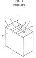
- strip-shaped auxiliary conductors f are formed on the open end surface d such that one auxiliary conductor f is located between resonators a and b, the other auxiliary conductor f is located between resonators b and c, and the auxiliary conductors f are electrically connected to an outer conductor e formed on the outer surface.
- the frequency characteristic of the dielectric filter shows an attenuation peak on the higher frequency side with respect to the center frequency.
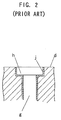
- a counterbore h is formed at the end of a through-hole g opened to the open end surface d, such that the diameter increases at the open end; and an inner conductor j covering the inner surface of the counterbore h is extended inward in the radial direction, to thereby increase the effective resonance length.
- This structure decreases the overall length of the dielectric filter as compared with a conventional dielectric filter having the same resonance length.
- dielectric filters having different shapes and characteristics are demanded.
- a dielectric filter which exhibits a filter characteristic having an attenuation peak on the higher-frequency side and which can be made compact.
- Such a demanded dielectric filter can be realized through combining the structure shown in FIG. 1 in which the strip-shaped conductors f are formed such that the filter characteristic has an attenuation peak, and the structure shown in FIG. 2 in which the overall length is shortened through formation of the counterbore h.
- the dielectric filter shown in FIG. 1 has the following drawback.
- the auxiliary conductors f and the outer conductor e are formed through a process in which a conductive material in the form of paste is applied, by means of screen printing, to each surface of a dielectric ceramic block in a predetermined pattern, followed by baking at a predetermined temperature.
- a conductive material in the form of paste In order to establish electrical connection between the auxiliary conductors f on the opened end surface d and the outer conductor e on the outer surface, the conductive material in the form of paste must be applied such that a conductive material layer on the opened end surface and a conductive material layer on a selected side surface must overlap each other at an edge portion where the opened end surface and the selected side surface intersect each other, so that mutual connection is established between the conductive material layers.
- each layer of applied conductive material is very thin and becomes thinner at the edge portion due to surface tension of the conductive material, when baking is performed in this state, a thin portion of the conductive material layer located at the edge portion easily breaks due to difference in thermal expansion coefficient between the dielectric ceramic block and the conductive material, with the result that so-called electrode breakage occurs at the edge portion.
- a conductive material in the form of paste is screen-printed on the flat open end surface. Therefore, the conductive material easily runs and spreads, which makes accurate formation of the auxiliary conductor f impossible.
- a first object of the, present invention is to provide a dielectric filter which has a shortened overall length and which can have a peak in its filter characteristic on the higher-frequency side with respect to the center frequency.
- Another object of the present invention is to provide a dielectric filter which has a structure that prevents electrode breakage which would otherwise occur at an edge portion and enables accurate formation of auxiliary conductors of a desired pattern.
- Still another object of the present invention is to provide a method of manufacturing a dielectric filter, which method prevents electrode breakage which would otherwise occur at an edge portion and enables accurate formation of auxiliary conductors of a desired pattern.
- a dielectric filter having three or more resonators which comprises: a dielectric ceramic block having three or more through-holes formed in parallel, the dielectric ceramic block having an open end surface to which one end of each through-hole is opened; an inner conductor covering the inner surface of each of the through-holes to thereby constitute the corresponding resonator; an outer conductor covering a predetermined outer surface of the dielectric ceramic block, excluding the open end surface; and input/output pads formed on one side surface of the dielectric ceramic block such that the pads are located near the open end surface and face resonators located at opposite ends, thereby establishing capacitance couplings therewith, wherein each of the through-holes of the resonators located at the opposite ends is provided with a counterbore which is formed at one end of the corresponding through-hole opened to the open end surface such that the diameter of the corresponding through-hole increases at the end; and an auxiliary conductor is disposed on the open end surface to face at
- each of through-holes constituting the resonators at the opposite ends has a counterbore which is formed at one end of the corresponding through-hole opened to the open end surface such that the diameter of the corresponding through-hole increases at the end. Therefore, the inner conductor covering the inner surface of the counterbore is extended inward in the radial direction, so that the effective resonance length increases. Thus, the lengths of the resonators at the opposite ends are shortened. Meanwhile, for at least one resonator other than the resonators at the opposite ends, an auxiliary conductor connected to the outer conductor on the side surface is disposed such that the auxiliary conductor surrounds the at least one resonator with an insulating gap formed therebetween.
- a capacitance C is produced between the auxiliary conductor and the inner conductor of the at least one resonator, and as will be described later, the length of the at least one resonator can be shortened by an amount corresponding to the capacitance C. Accordingly, the resonance length of the at least one resonator can be rendered the same as those of the resonators at the opposite ends upon generation of the capacitance C which is adjusted to a desired value through adjustment of the insulating gap and the length of the arcuate edge portion of the auxiliary conductor surrounding the at least one resonator. Thus, the overall length of the dielectric filter can be shortened. Further, the dielectric filter has a filter characteristic in which an attenuation peak appears on the higher-frequency side.
- the auxiliary conductor has an opened configuration such that the auxiliary conductor has an opening which is opened toward the side surface on which the input/output pads are not formed; and a second auxiliary conductor extends toward the opening from a portion of the outer conductor located on the side surface on which the input/output pads are not provided, such that the inner edge of the second auxiliary conductor faces the corresponding resonator with an insulating gap formed therebetween.
- a trap resonator may be disposed at one end of the dielectric ceramic block such that the trap resonator is located adjacent to at least one of the resonators disposed at the opposite ends.
- the inner surface of a through-hole of the trap resonator is covered with an inner conductor, and a counterbore is formed at one end of the through-hole opened to the open end surface such that the diameter of the through-hole increases at the end.
- a dielectric filter having a plurality of resonators which comprises: a dielectric ceramic block having a plurality of through-holes formed in parallel, the dielectric ceramic block having an open end surface to which one end of each through-hole is opened; an inner conductor covering the inner surface of each of the through-holes to thereby constitute the corresponding resonator; an outer conductor covering a predetermined outer surface of the dielectric ceramic block, excluding the open end surface; and an auxiliary conductor formed on the open end surface and having a predetermined pattern, the auxiliary conductor being electrically connected with a portion of the outer conductor located on one side surface of the dielectric ceramic block, wherein the auxiliary conductor is formed of a conductive material placed in a concave portion which has a pattern corresponding to the pattern of the auxiliary conductor and is formed on the open end surface.
- the auxiliary conductor of a desired pattern can be formed accurately.
- a method of manufacturing a dielectric filter comprising the steps of: press-forming ceramic powder to obtain a green body having a shape of a substantially rectangular prism in such a manner that a concave portion having a predetermined shape is formed on one end surface which is to serve as an open end surface; sintering the green body to obtain a dielectric ceramic block; charging a conductive material in the form of paste in the concave portion; applying a conductive material onto a predetermined outer surface of the dielectric ceramic block, excepting the end surface which is to serve as the open end surface; and baking the conductive materials to thereby form an outer conductor on the outer surface of the dielectric ceramic block and form an auxiliary conductor in the concave portion of the open end surface such that an outer end of the auxiliary conductor is electrically connected to a portion of the outer conductor located on one side surface of the dielectric ceramic block.
- a concave portion of predetermined shape can easily be formed in the green body simultaneously with formation of the green body, through employment of a mold which has on its inner surface a projection corresponding to the concave portion.
- a dielectric filter having three or more resonators which comprises: a dielectric ceramic block having three or more through-holes formed in parallel, the dielectric ceramic block having an open end surface to which one end of each through-hole is opened; an inner conductor covering the inner surface of each of the through-holes to thereby constitute the corresponding resonator; an outer conductor covering a predetermined outer surface of the dielectric ceramic block, excluding the open end surface; and input/output pads formed on one side surface of the dielectric ceramic block such that the pads are located near the open end surface and face resonators located at opposite ends, thereby establishing capacitance couplings therewith, wherein each of the through-holes of the resonators located at the opposite ends is provided with a counterbore which is formed at one end of the corresponding through-hole opened to the open end surface such that the diameter of the corresponding through-hole increases at the end; an auxiliary conductor is disposed on the open end surface to face the
- the overall length of the dielectric filter can be shortened, and the dielectric filter has a filter characteristic in which an attenuation peak appears on the higher-frequency side.
- the conductive material since the shape of the conductive material is defined by the concave portion; i.e., flow of the conductive material is restricted by the concave portion, the conductive material neither runs nor spreads. Moreover, since the auxiliary conductor can be formed accurately such that the insulating gap has an intended size and the arcuate edge portion of the auxiliary conductor surrounding the at least one resonator has an intended length, an intended capacitance C can be obtained reliably. Furthermore, since the auxiliary conductor has a thickness corresponding to the depth of the concave portion, the end surface of the auxiliary conductor facing the at least one resonator has a larger area, so that a larger capacitance C can be generated.
- the dielectric filter can be manufactured by the above-described method.
- the edge portion at which the bottom surface of the concave portion intersects with the corresponding side surface of the dielectric ceramic block is covered with a thick layer of the conductive material. Accordingly, the layers at the edge portion each attain a desired level of strength during a subsequent baking step. Thus, there can be prevented electrode breakage which would otherwise occur at the edge portion due to a difference in thermal expansion coefficient between the dielectric ceramic block and the conductive material.
- the auxiliary conductor has an opened configuration such that the auxiliary conductor has an opening which is opened toward the side surface on which the input/output pads are not formed; a second auxiliary conductor extends toward the opening from a portion of the outer conductor located on the side surface on which the input/output pads are not provided, such that the inner edge of the second auxiliary conductor faces the corresponding resonator with an insulating gap formed therebetween; and the second auxiliary conductor is formed of a conductive material placed in a second concave portion which has a pattern corresponding to the pattern of the second auxiliary conductor and is formed on the open end surface.
- the second auxiliary conductor can be formed accurately such that the insulating gap has an intended size and the second auxiliary conductor has an intended shape. Furthermore, since the end surface of the second auxiliary conductor facing the corresponding resonator has a larger area, a larger capacitance C can be generated. In addition, electrode breakage does not occur at the edge portion.
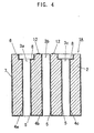
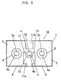
- FIGS. 3 to 5 show a dielectric filter 1A according to a first embodiment of the present invention.
- the dielectric filter 1A three resonators 3a, 3b, and 3c are formed in parallel in a single dielectric ceramic block 2.
- the dielectric ceramic block 2 has the shape of a rectangular prism and is made of a dielectric ceramic such as BaO-TiO 2 ceramic or BaO-TiO 2 -(rare earth oxide) ceramic.
- the resonators 3a, 3b, and 3c are formed parallel to each other such that they are oriented in the same direction.
- the resonators 3a, 3b, and 3c are formed by coating the inner surfaces of through-holes 4a, 4b, and 4c with inner conductors 5.
- the outer surface of the dielectric ceramic block 2 is coated with an outer conductor 7, except for an open end surface 6 to which upper ends of the through-holes 4a, 4b, and 4c are opened.
- the outer conductor 7 serves as a shield electrode.
- the left-hand resonator 3a and the right-hand resonator 3c have counterbores 8 which are formed at the upper ends of the through-hole 4a and 4c opened to the open end surface 6 such that the diameters of the through-holes 4a and 4c increase at the upper ends.
- the inner surfaces of the counterbores 8 are also covered with inner conductors 5.
- the inner conductors 5 covering the inner surfaces of the counterbores 8 are extended inward in the radial direction, so that the inner conductors 5 each extend over an increased distance, and the effective resonance length increases.
- the lengths of the resonators 3a and 3c are shortened as compared with a dielectric filter which has the same resonance length and in which the counterbores 8 are not formed.
- the resonance length of the resonators 3a and 3c is set to a length corresponding to ⁇ /4, where ⁇ is a resonance frequency.
- Input/output pads 9 are formed on one side surface of the dielectric ceramic block 2 such that the pads 9 are located near the open end surface 6 and face the left-hand and right-hand resonators 3a and 3c.
- the input/output pads 9 are isolated from the outer conductor 7 by means of rectangular conductor-removed portions 10. Thus, capacitance coupling is established between the resonator 3a and the corresponding input/output pad 9 and between the resonator 3c and the corresponding input/output pad 9.
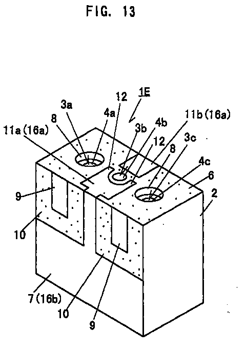
- a first auxiliary conductor 11a and a second auxiliary conductor 11b are provided on the upper end surface 6 to face the center resonator 3b.
- the first auxiliary conductor 11a is forked and has two branch portions 12, one of which is located between the resonators 3a and 3b, and the other of which is located between the resonators 3b and 3c.
- At the inner edge of the first auxiliary conductor 11a in proximity to the through-hole 4b is formed an arcuate edge portion 13 which is concentric with the through-hole 4b.
- the first auxiliary conductor 11a is disposed such that the arcuate edge portion 13 surrounds the through-hole 4b with an insulating gap s formed therebetween.
- the outer end of the first auxiliary conductor 11a is connected to a portion of the outer conductor 7 located on the side surface on which the input/output pads 9 are provided.
- the first auxiliary conductor 11a has an opened configuration such that the arcuate edge portion 13 forms an opening which is opened toward the side surface on which the input/output pads 9 are not formed.
- the second auxiliary conductor 11b is extended toward the opening from a portion of the outer conductor 7 located on the side surface on which the input/output pads 9 are not provided, such that the inner edge of the second auxiliary conductor 11b faces the resonator 3b with an insulating gap s' formed therebetween.
- the first auxiliary conductor 11a and the second auxiliary conductor 11b can be formed through a process in which a conductive material in the form of paste is screen-printed on the open end surface 6 in a predetermined pattern.
- the resonance length of the center resonator 3b can be rendered the same as those of the left-hand and right-hand resonators 3a and 3c upon generation of the capacitance C which is adjusted to a desired value through adjustment of the insulating gaps s and s' and the length of the arcuate edge portion 13 of the first auxiliary conductor 11a surrounding the resonator 3b.
- the center resonator 3b is shortened to have the same length as those of the left-hand and right-hand resonators 3a and 3c, whereby the overall length of the dielectric filter 1 can be shortened.
- the dielectric filter 1 has a filter characteristic as shown in FIG. 6 in which a frequency characteristic curve x involves an attenuation peak m on the higher-frequency side with respect to the center frequency, because the two branch portions 12 of the first auxiliary conductor 11a provided on the open end surface 6 are located between the resonators 3a and 3b and between the resonators 3b and 3c, respectively, and the outer end of the first auxiliary conductor 11a is connected to a portion of the outer conductor 7 located on the side surface on which the input/output pads 9 are provided. Therefore, the dielectric filter 1 can be designed to have a peak on the higher-frequency side through provision of the branch portions 12.
- FIG. 6 also shows a curve y indicating the reflection wave characteristic measured simultaneously.
- the second auxiliary conductor 11b is provided on the open end surface 6 only for the purpose of increasing the capacitance C. Therefore, when a desired capacitance C is obtained by provision of the first auxiliary conductor 11a only, provision of the second auxiliary conductor 11b is unnecessary. Further, the first, auxiliary conductor 11a may be formed to have an annular edge portion which surrounds the entire circumference of the through-hole 4b of the resonator 3b.
- a three-stage dielectric filter composed of three resonators 3a, 3b, and 3c is described.
- the present invention can be applied to a multi-stage dielectric filter having four or more stages.
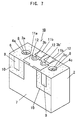
- FIG. 7 shows a four-stage dielectric filter 1B according to a second embodiment of the present invention.
- four resonators 3a, 3b, 3b', and 3c are formed in parallel in a single dielectric ceramic block 2.
- the left-hand resonator 3a and the right-hand resonator 3c have counterbores 8 which are formed at the upper ends of the through-hole 4a and 4c opened to the open end surface 6 such that the diameters of the through-holes 4a and 4c increase at the upper ends.
- a first auxiliary conductor 11a is provided on the upper end surface 6 to face the center resonators 3b and 3b', respectively.
- the first auxiliary conductor 11a is forked and has three branch portions 12.
- the first branch portion is located between the resonators 3a and 3b
- the second branch portion is located between the resonators 3b and 3b'
- the third branch portion is located between the resonators 3b' and 3c.
- the outer end of the first auxiliary conductor 11a is connected to a portion of the outer conductor 7 located on the side surface on which the input/output pads 9 are provided. If necessary, auxiliary conductors 11b are provided.
- the second auxiliary conductors 11b extend from the outer conductor 7 on the side surface on which the input/output pads 9 are not provided.
- the counterbores 8 of the left-hand and right-hand resonators 3a and 3c increase the effective resonance lengths of the resonators 3a and 3c, so that the lengths of the resonators 3a and 3c can be reduced.
- the lengths of the center-side resonators 3b and 3b' can be reduced by the action of the capacitance C of the open end surface 6 generated by the first auxiliary conductor 11a singly or in cooperation with the auxiliary conductors 11b. Therefore, the overall length of the dielectric filter 1B can be decreased.
- the dielectric filter 1B due to presence of the branch portions 12 of the first auxiliary conductor 11a, the dielectric filter 1B has a peak in frequency characteristic on the higher-frequency side with respect to the center frequency.
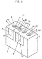
- FIG. 8 shows a dielectric filter 1C according to a third embodiment of the present invention.
- the dielectric filter 1C four resonators 3a, 3b, 3c, and 3d are formed in parallel in a single dielectric ceramic block 2.
- Three adjacent resonators 3a, 3b, and 3c (the three left-hand resonators in FIG. 8) constitute a three-stage dielectric filter, and the resonator 3d located at the right end serves as a trap resonator.
- the three-stage dielectric filter is completed through formation of the input/output pads 9 on one side surface of the dielectric ceramic block 2 such that the pads 9 are located near the open end surface 6 and face the left-hand and right-hand resonators 3a and 3c.
- the resonators 3a, 3b, and 3c have the same structures as those of the resonators 3a, 3b, and 3c in the first embodiment. Therefore, the same portions are denoted by the same reference numerals, and their descriptions are omitted for avoiding redundancy.
- the resonator 3d serving as a trap resonator has the same structure as those of the resonators 3a and 3c. That is, the inner surface of the through-hole 4d formed in the dielectric ceramic block 2 is covered with an inner conductor 5, and a counterbore 8 is formed at the upper end of the through-hole 4d opened to the open end surface 6 such that the diameter of the through-hole 4d increases at the upper end. Thus, the length of the resonator 3d is shortened as well.
- the resonator 3d serving as a trap resonator is disposed at the end of the dielectric ceramic block 2 such that inter-stage coupling is established between the resonator 3b and the resonator 3c at the preceding stage. Therefore, a trap effect is produced at a self-resonance frequency outside the pass band, whereby spurious signals can be attenuated for elimination thereof.
- the resonator 3d serving as a trap resonator is disposed at the end of the dielectric ceramic block 2 to be located adjacent to the resonator 3c, which is an output-side resonator.
- the resonator 3d serving as a trap resonator may be disposed at the opposite end of the dielectric ceramic block 2 to be located adjacent to the resonator 3a, which is an input-side resonator.
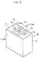
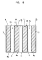
- FIGS. 9 and 10 show a dielectric filter 1D according to a fourth embodiment of the present invention.
- the dielectric filter 1D three resonators 3a, 3b, and 3c are formed in parallel in a single dielectric ceramic block 2 to thereby form a three-stage dielectric filter.
- the dielectric ceramic block 2 has the shape of a rectangular prism and is made of a dielectric ceramic such as BaO-TiO 2 ceramic or BaO-TiO 2 -(rare earth oxide) ceramic.
- the resonators 3a, 3b, and 3c are formed parallel to each other such that they are oriented in the same direction.
- the resonators 3a, 3b, and 3c are formed by coating the inner surfaces of through-holes 4a, 4b, and 4c with inner conductors 5.
- the outer surface of the dielectric ceramic block 2 is coated with an outer conductor 7, except for an open end surface 6 to which upper ends of the through-holes 4a, 4b, and 4c are opened.
- the outer conductor 7 serves as a shield electrode.
- auxiliary conductor 11 Two strip-shaped auxiliary conductor 11 are provided on the open end surface 6 such that one auxiliary conductor 11 crosses the space between the resonators 3a and 3b and the other auxiliary conductor 11 crosses the space between the resonators 3b and 3c.
- the opposite ends of each auxiliary conductor 11 are connected to the outer conductor 7 provided on the outer surface.
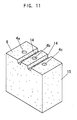
- the auxiliary conductor 11 is formed through a process in which concave portions 14 (see FIG. 11) are formed on the open end surface 6 in the same pattern as that of the auxiliary conductors 11, and a conductive material is charged into the concave portions 14.
- the dielectric filter 1D Next will be described a method of manufacturing the dielectric filter 1D.
- powder of dielectric ceramic such as BaO-TiO 2 ceramic or BaO-TiO 2 -(rare earth oxide) ceramic
- the mold used for press forming has on its inner surface convex portions corresponding to the concave portions 14.
- the concave portions 14 of a predetermined shape are formed on one end surface of the green body 15, which surface is to serve as the open end surface 6, such that the outer ends of each concave portion 14 are opened to the respective side surfaces of the green body 15.
- the through-holes 4a, 4b, and 4c are simultaneously formed in the green body 15 by means of shaft-shaped cores disposed within the mold. Subsequently, the green body 15 is sintered at a temperature of about 1200 to 1300°C, whereby the dielectric ceramic block 2 is obtained.
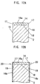
- a conductive material 16a such as silver, in the form of paste is charged into the concave portions 14 to a thickness corresponding to the depth of the concave portions 14.
- the charging of the conductive material 16a can be performed through screen printing or any other appropriate process.
- a layer of the conductive material 16a is formed in each concave portion 14 such that the opposite ends 17 of the layer become flush with the respective side surfaces of the dielectric ceramic block 2.
- a conductive material 16b in the form of paste is applied onto the outer surface of the dielectric ceramic block 2, excepting the open end surface 6, by means of screen printing.
- a layer of the conductive material 16b formed on each side surface of the dielectric ceramic block 2 is connected to the corresponding end surface 17 of the layer of the conductive material 16a charged into each concave portion 14.
- each edge portion 20 at which a bottom surface 18 of each concave portion 14 and the corresponding side surface of the dielectric ceramic block 2 intersect with each other is covered with thick layers.
- a conductive material in the form of paste ⁇ which is to serve as the inner conductor 5 ⁇ is applied onto the inner surface of the through-holes 4a, 4b, and 4c by means of vacuum suction or the like.
- the dielectric ceramic block 2 carrying the conductive materials is baked at a predetermined temperature.
- the conductive material 16b forms the outer conductor 7 on the outer surface of the dielectric ceramic block 2
- the conductive material 16a forms the auxiliary conductors 11 within the concave portions 14 of the open end surface 6 such that the opposite ends of the auxiliary conductors 11 are in electrical communication with portions of the outer conductor 7 located on the opposite side surfaces of the dielectric ceramic block 2.
- the dielectric filter 1D shown in FIG. 9 is obtained.
- the conductive material 16a in the form of paste is charged into the concave portions 14 ⁇ which have the same pattern as that of the auxiliary conductors 11 and are formed on the open end surface 6 ⁇ to a thickness corresponding to the depth of the concave portions 14, such that the ends 17 of the layer of the conductive material 16a become flush with the respective side surfaces of the dielectric ceramic block 2; and a conductive material 16b in the form of paste is applied onto the outer surface of the dielectric ceramic block 2, such that a layer of the conductive material 16b formed on each side surface of the dielectric ceramic block 2 is connected to the corresponding end surface 17 of the layer of the conductive material 16a.
- each edge portion 20 at which the bottom surface 18 of each concave portion 14 intersects with the corresponding side surface 19 of the dielectric ceramic block 2 is covered with the layers of the conductive materials 16a and 16b each having a desired thickness. Accordingly, the layers at the edge portion 20 each attain a desired level of strength during the subsequent baking step. Thus, there can be prevented electrode breakage which would otherwise occur at the edge portion 20 due to a difference in thermal expansion coefficient between the dielectric ceramic block 2 and the conductive materials 16a and 16b.
- the conductive material 16a in the form of paste is charged into the concave portions 14 formed on the open end surface 6. Since the shape of the conductive material 16a is defined by the concave portions 14; i.e., flow of the conductive material 16a is restricted by the concave portions 14, the conductive material 16a neither runs nor spreads. Thus, the auxiliary conductors 11 of a desired pattern can be formed accurately.
- input/output pads which are coupled with the resonators 3a and 3c by means of capacitance coupling may be formed during application of the conductive material 16b.
- the conductive material 16b is screen printed in a predetermined pattern on one side surface of the dielectric ceramic block 2 such that the input/output pads are formed on the side surface while being isolated from the outer conductor 7.
- a three-stage dielectric filter composed of three resonators 3a, 3b, and 3c is described.
- the structure feature of the present embodiment i.e., the provision of the strip-shaped auxiliary conductors 11 ⁇ which enables the dielectric filter to have a peak in its frequency characteristic on the higher-frequency side ⁇ can be applied to a two-stage dielectric filter or a multi-stage dielectric filter having four or more stages.
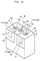
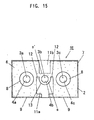
- FIGS. 13 to 15 show a dielectric filter 1E according to a fifth embodiment of the present invention. Since the dielectric filter 1E has a structure similar to that of the first embodiment, the structure of the dielectric filter 1E is not described here.
- the dielectric filter 1E is produced in the same manner as in the first embodiment, except for the step of forming the first auxiliary conductor 11a and the second auxiliary conductor 11b. That is, the auxiliary conductors 11a and 11b are formed through a process in which concave portions 14a and 14b having the same patterns as those of the auxiliary conductors 11a and 11b are formed on the open end surface 6 (see FIG. 16), and a conductive material is charged into the concave portions 14a and 14b.
- the dielectric filter 1E When powder of dielectric ceramic is press-formed so as to obtain a green body having the shape of a substantially rectangular prism, there is used a mold which has on its inner surface convex portions corresponding to the concave portions 14a and 14b.
- the concave portions 14a and 14b each having a predetermined shape are formed on one end surface of the green body 15, which surface is to serve as the open end surface 6, such that the outer ends of the concave portions 14a and 14b are opened to the corresponding side surfaces of the green body 15.
- the through-holes 4a, 4b, and 4c are simultaneously formed in the green body 15 by means of shaft-shaped cores disposed within the mold.
- counterbores 8 are formed at the upper ends of the through-holes 4a and 4c by means of projections which are disposed within the mold and have a shape corresponding to that of the counterbores 8.
- a conductive material 16a such as silver, in the form of paste is charged into the concave portions 14a and 14b to a thickness corresponding to the depth of the concave portions 14a and 14b.
- the charging of the conductive material 16a can be performed through screen printing or any other appropriate process.
- a layer of the conductive material 16a is formed in each of the concave portions 14a and 14b such that the outer end 17 of the layer become flush with the corresponding side surface 19 of the dielectric ceramic block 2.
- a conductive material 16b in the form of paste is applied onto the outer surface of the dielectric ceramic block 2, excepting the open end surface 6, by means of screen printing.
- input/output pads 9 are printed in a predetermined pattern on the side surface 19 of the dielectric ceramic block 2 to which the outer end of the concave portion 14a is opened.
- each edge portion 20 at which a bottom surface 18 of the concave portion 14a or 14b and the corresponding side surface of the dielectric ceramic block 2 intersect with each other is covered with thick layers. That is, there is no possibility that the thicknesses of the layers of the conductive materials 16a and 16b decrease at the edge portions due to surface tensions of the conductive materials 16a and 16b. Therefore, a desired layer thickness can be secured.
- a conductive material in the form of paste ⁇ which is to serve as the inner conductor 5 ⁇ is applied onto the inner surfaces of the through-holes 4a, 4b, and 4c, as well as onto the inner surface of the counterbores 8, by means of vacuum suction or the like.
- the dielectric ceramic block 2 carrying the conductive materials is baked at a predetermined temperature.
- the conductive material 16b forms the outer conductor 7 on the outer surface of the dielectric ceramic block 2
- the conductive material 16a forms the auxiliary conductors 11a and 11b within the concave portions 14a and 14b of the open end surface 6 such that the outer ends of the auxiliary conductors 11a and 11b are in electrical communication with portions of the outer conductor 7 located on the opposite side surfaces of the dielectric ceramic block 2.
- the dielectric filter 1E shown in FIG. 13 is obtained.
- the conductive material 16a in the form of paste is charged into the concave portions 14a and 14b ⁇ which have the same patterns as those of the auxiliary conductors 11a and 11b and are formed on the open end surface 6 ⁇ to a thickness corresponding to the depth of the concave portions 14a and 14b, such that the outer end surface 17 of the layer of the conductive material 16a becomes flush with the corresponding side surfaces of the dielectric ceramic block 2; and the conductive material 16b in the form of paste is applied onto the outer surface of the dielectric ceramic block 2, such that a layer of the conductive material 16b formed on each side surface of the dielectric ceramic block 2 is connected to the corresponding outer end surface 17 of the layer of the conductive material 16a over a relatively large area.
- each edge portion 20 at which a bottom surface 18 of the concave portion 14a or 14b intersects with the corresponding side surface 19 of the dielectric ceramic block 2 is covered with the layers of the conductive materials 16a and 16b each having a desired thickness. Accordingly, the layers at the edge portion 20 each attain a desired level of strength during the subsequent baking step. Thus, there can be prevented electrode breakage which would otherwise occur at the edge portion 20 due to a difference in thermal expansion coefficient between the dielectric ceramic block 2 and the conductive materials 16a and 16b.
- the dielectric filter of the preset embodiment provides the following advantages, as well as those provided by the dielectric filter of the first embodiment.
- the conductive material 16a in the form of paste is charged into the concave portions 14a and 14b formed on the open end surface 6. Since the shape of the conductive material 16a is defined by the concave portions 14a and 14b; i.e., flow of the conductive material 16a is restricted by the concave portions 14a and 14b, the conductive material 16a neither runs nor spreads.
- auxiliary conductor 11a and 11b can be formed accurately such that the above-described insulating gaps s and s' have an intended size and the arcuate edge portion of the auxiliary conductor 11a surrounding the resonator 3b has an intended length, an intended capacitance C can be obtained reliably.
- the auxiliary conductors 11a and 11b have a thickness corresponding to the depth of the concave portions 14a and 14b, the end surfaces of the auxiliary conductors 11a and 11b facing the resonator 3b each have a larger area, as compared with the case of the first embodiment, a larger capacitance C can be generated.
- FIGS. 18 and 19 show a four-stage dielectric filter 1F according to a sixth embodiment of the present invention. Since the dielectric filter 1F has a structure similar to that of the second embodiment, the structure of the dielectric filter 1F is not described here.
- the first auxiliary conductor 11a and the second conductors 11b are formed through a process in which concave portions 14a and 14b having the same patterns as those of the auxiliary conductors 11a and 11b are formed on the open end surface 6 (see FIG. 19), and a conductive material is charged into the concave portions 14a and 14b.
- the first auxiliary conductor 11a and the second auxiliary conductors 11b can be formed accurately so as to obtain a desired capacitance C, and a larger capacitance C can be generated.
- the dielectric filter of the present embodiment provides the same advantages as those provided by the second embodiment.
Landscapes
- Engineering & Computer Science (AREA)
- Manufacturing & Machinery (AREA)
- Physics & Mathematics (AREA)
- Electromagnetism (AREA)
- Control Of Motors That Do Not Use Commutators (AREA)
Abstract
Description
Claims (7)
- A dielectric filter having three or more resonators (3a, 3b, 3b', 3c), comprising a dielectric ceramic block (2) having three or more through-holes (4a, 4b, 4b', 4c) formed in parallel, the dielectric ceramic block (2) having an open end surface (6) to which one end of each through-hole (4a, 4b, 4b', 4c) is opened; an inner conductor (5) covering the inner surface of each of the through-holes (4a, 4b, 4b', 4c) to thereby constitute the corresponding resonator (3a, 3b, 3b', 3c); an outer conductor (7) covering a predetermined outer surface of the dielectric ceramic block (2), excluding the open end surface (6); and input/output pads (9) formed on one side surface of the dielectric ceramic block (2) such that the pads (9) are located near the open end surface (6) and face resonators (3a, 3c) located at opposite ends, thereby establishing capacitance couplings therewith, characterized in thateach of the through-holes (4a, 4c) of the resonators (3a, 3c) located at the opposite ends is provided with a counterbore (8) which is formed at one end of the corresponding through-hole opened to the open end surface (6) such that the diameter of the corresponding through-hole (4a, 4c) increases at the end; andan auxiliary conductor (11a) is disposed on the open end surface (6) to face at least one resonator (3b) excepting the resonators (3a, 3c) at the opposite ends, the auxiliary conductor (11a) being forked and having at least two branch portions (12), each being located between adjacent resonators (e.g., 3a, 3b) and the auxiliary conductor (11a) surrounding the at least one resonator (3b) with an insulating gap formed therebetween and being connected to a portion of the outer conductor (7) located on the side surface on which the input/output pads (9) are provided.
- A dielectric filter according to claim 1, characterized in that the auxiliary conductor (11a) has an opened configuration such that the auxiliary conductor (11a) has an opening which is opened toward the side surface on which the input/output pads (9) are not formed; and a second auxiliary conductor (11b) extends toward the opening from a portion of the outer conductor (7) located on the side surface on which the input/output pads (9) are not provided, such that the inner edge of the second auxiliary conductor (11b) faces the corresponding resonator (3b, 3c) with an insulating gap formed therebetween.
- A dielectric filter according to claim 1 or claim 2, characterized in that a trap resonator (3d) is disposed at one end of the dielectric ceramic block (2) such that the trap resonator (3d) is located adjacent to at least one of the resonators (3a, 3c) disposed at the opposite ends, the inner surface of a through-hole (4d) of the trap resonator (3d) being covered with an inner conductor (5), and a counterbore (8) being formed at one end of the through-hole (4d) opened to the open end surface (6) such that the diameter of the through-hole (4d) increases at the end.
- A dielectric filter according to claim 1, characterized in thatthe auxiliary conductor (11a) is formed of a conductive material (16b) placed in a concave portion (14a) which has a pattern corresponding to the pattern of the auxiliary conductor (11a) and is formed on the open end surface (6).
- A dielectric filter according to claim 4, characterized in that the auxiliary conductor (11a) has an opened configuration such that the auxiliary conductor (11a) has an opening which is opened toward the side surface on which the input/output pads (9) are not formed; a second auxiliary conductor (11b) extends toward the opening from a portion of the outer conductor (7) located on the side surface on which the input/output pads (9) are not provided, such that the inner edge of the second auxiliary conductor (11b) faces the corresponding resonator (e.g. 3b) with an insulating gap formed therebetween; and the second auxiliary conductor (11b) is formed of a conductive material (16a) placed in a second concave portion (14b) which has a pattern corresponding to the pattern of the second auxiliary conductor (11b) and is formed on the open end surface (6).
- A dielectric filter having a plurality of resonators (3a, 3b, 3c), comprising a dielectric ceramic block (2) having a plurality of through-holes (4a, 4b, 4c) formed in parallel, the dielectric ceramic block (2) having an open end surface (6) to which one end of each through-hole (4a, 4b, 4c) is opened; an inner conductor (5) covering the inner surface of each of the through-holes (4a, 4b, 4c) to thereby constitute the corresponding resonator (3a, 3b, 3c); an outer conductor (7) covering a predetermined outer surface of the dielectric ceramic block (2), excluding the open end surface (6); and an auxiliary conductor (11) formed on the open end surface (6) and having a predetermined pattern, the auxiliary conductor (11) being electrically connected with a portion of the outer conductor (7) located on one side surface of the dielectric ceramic block (2), characterized in thatthe auxiliary conductor (11) is formed of a conductive material placed in a concave portion (14) which has a pattern corresponding to the pattern of the auxiliary conductor (11) and is formed on the open end surface (6).
- A method of manufacturing a dielectric filter, characterized by comprising the steps of:press-forming ceramic powder to obtain a green body (15) having a shape of a substantially rectangular prism in such a manner that a concave portion (14, 14a, 14b) having a predetermined shape is formed on one end surface which is to serve as an open end surface (6);sintering the green body (15) to obtain a dielectric ceramic block (2);charging a conductive material (16a) in the form of paste in the concave portion (14, 14a, 14b);applying a conductive material (16b) onto a predetermined outer surface of the dielectric ceramic block (2), excepting the end surface which is to serve as the open end surface (6); andbaking the conductive materials (16a, 16b) to thereby form an outer conductor (7) on the outer surface of the dielectric ceramic block (2) and form an auxiliary conductor (11, 11a 11b) in the concave portion (14, 14a, 14b) of the open end surface (6) such that an outer end of the auxiliary conductor (11, 11a 11b) is electrically connected to a portion of the outer conductor (7) located on one side surface of the dielectric ceramic block (2).
Applications Claiming Priority (4)
| Application Number | Priority Date | Filing Date | Title |
|---|---|---|---|
| JP27066799A JP2001094305A (en) | 1999-09-24 | 1999-09-24 | Dielectric filter |
| JP27066799 | 1999-09-24 | ||
| JP34222299 | 1999-12-01 | ||
| JP34222299A JP2001160701A (en) | 1999-12-01 | 1999-12-01 | Dielectric filter and method of manufacturing the dielectric filter |
Publications (3)
| Publication Number | Publication Date |
|---|---|
| EP1087457A2 true EP1087457A2 (en) | 2001-03-28 |
| EP1087457A3 EP1087457A3 (en) | 2002-06-12 |
| EP1087457B1 EP1087457B1 (en) | 2006-12-13 |
Family
ID=26549308
Family Applications (1)
| Application Number | Title | Priority Date | Filing Date |
|---|---|---|---|
| EP00307378A Expired - Lifetime EP1087457B1 (en) | 1999-09-24 | 2000-08-29 | Dielectric filter and method of manufacturing the same |
Country Status (3)
| Country | Link |
|---|---|
| US (1) | US6501347B1 (en) |
| EP (1) | EP1087457B1 (en) |
| DE (1) | DE60032300T2 (en) |
Cited By (7)
| Publication number | Priority date | Publication date | Assignee | Title |
|---|---|---|---|---|
| US6816034B2 (en) | 2002-03-29 | 2004-11-09 | Ngk Spark Plug Co., Ltd. | Electronic part such as dielectric filter or duplexer and method of forming an electrode of such an electronic part |
| US6949987B2 (en) | 2002-03-29 | 2005-09-27 | Ngk Spark Plug Co., Ltd | Dielectric electronic component with attenuation adjustment electrode and method of adjusting attenuation characteristics of the same |
| USD805476S1 (en) * | 2016-12-20 | 2017-12-19 | Cirocomm Technology Corp. | Dielectric filter |
| USD805475S1 (en) * | 2016-12-20 | 2017-12-19 | Cirocomm Technology Corp. | Dielectric filter |
| USD805477S1 (en) * | 2016-12-20 | 2017-12-19 | Cirocomm Technology Corp. | Dielectric filter |
| USD806032S1 (en) * | 2016-12-20 | 2017-12-26 | Cirocomm Technology Corp. | Dielectric filter |
| CN121192390A (en) * | 2022-07-18 | 2025-12-23 | 苏州立讯技术有限公司 | Cavity Filter |
Families Citing this family (1)
| Publication number | Priority date | Publication date | Assignee | Title |
|---|---|---|---|---|
| CN115548604A (en) * | 2021-06-29 | 2022-12-30 | 华为技术有限公司 | A filtering device and communication system |
Family Cites Families (21)
| Publication number | Priority date | Publication date | Assignee | Title |
|---|---|---|---|---|
| JPS60114004A (en) | 1983-11-25 | 1985-06-20 | Murata Mfg Co Ltd | Dielectric coaxial resonator |
| JPS60152102A (en) * | 1984-01-19 | 1985-08-10 | Murata Mfg Co Ltd | Distributed constant type filter |
| JPS60152012A (en) | 1984-01-19 | 1985-08-10 | Sharp Corp | Transformer |
| JPS62103302A (en) | 1985-10-28 | 1987-05-13 | Kobe Steel Ltd | Manufacture of sintered hard metallic parts |
| US4879533A (en) * | 1988-04-01 | 1989-11-07 | Motorola, Inc. | Surface mount filter with integral transmission line connection |
| US4985690A (en) * | 1988-07-07 | 1991-01-15 | Matsushita Electric Industrial Co., Ltd. | Dielectric stepped impedance resonator |
| JPH04360301A (en) * | 1991-06-06 | 1992-12-14 | Mitsubishi Electric Corp | Strip line |
| JP2738409B2 (en) * | 1992-02-14 | 1998-04-08 | 宇部興産株式会社 | How to attach the case to the dielectric filter |
| JP2936443B2 (en) | 1992-04-30 | 1999-08-23 | 日本特殊陶業株式会社 | Dielectric filter |
| JPH0711002U (en) | 1993-07-23 | 1995-02-14 | 日本特殊陶業株式会社 | Dielectric filter |
| JP3319121B2 (en) * | 1994-02-22 | 2002-08-26 | 株式会社村田製作所 | Dielectric filter |
| JP3448341B2 (en) | 1994-04-11 | 2003-09-22 | 日本特殊陶業株式会社 | Dielectric filter device |
| JPH0964616A (en) * | 1995-08-29 | 1997-03-07 | Fuji Elelctrochem Co Ltd | Method for manufacturing dielectric filter |
| US5684439A (en) * | 1995-10-10 | 1997-11-04 | Motorola, Inc. | Half wave ceramic filter with open circuit at both ends |
| JPH09219605A (en) | 1996-02-09 | 1997-08-19 | Ngk Spark Plug Co Ltd | Dielectric filter and resonance frequency adjusting method thereof |
| US5793267A (en) * | 1996-03-07 | 1998-08-11 | Murata Manufacturing Co., Ltd. | Dielectric block filter having first and second resonator arrays coupled together |
| JP3014638B2 (en) * | 1996-03-15 | 2000-02-28 | ティーディーケイ株式会社 | Dielectric filter |
| JPH09312506A (en) | 1996-05-23 | 1997-12-02 | Ngk Spark Plug Co Ltd | Dielectric filter |
| US5929721A (en) * | 1996-08-06 | 1999-07-27 | Motorola Inc. | Ceramic filter with integrated harmonic response suppression using orthogonally oriented low-pass filter |
| JPH10126106A (en) * | 1996-10-18 | 1998-05-15 | Ngk Spark Plug Co Ltd | Dielectric filter |
| JPH1168407A (en) * | 1997-08-21 | 1999-03-09 | Murata Mfg Co Ltd | Dielectric filter |
-
2000
- 2000-08-29 DE DE60032300T patent/DE60032300T2/en not_active Expired - Lifetime
- 2000-08-29 EP EP00307378A patent/EP1087457B1/en not_active Expired - Lifetime
- 2000-08-31 US US09/652,016 patent/US6501347B1/en not_active Expired - Fee Related
Cited By (7)
| Publication number | Priority date | Publication date | Assignee | Title |
|---|---|---|---|---|
| US6816034B2 (en) | 2002-03-29 | 2004-11-09 | Ngk Spark Plug Co., Ltd. | Electronic part such as dielectric filter or duplexer and method of forming an electrode of such an electronic part |
| US6949987B2 (en) | 2002-03-29 | 2005-09-27 | Ngk Spark Plug Co., Ltd | Dielectric electronic component with attenuation adjustment electrode and method of adjusting attenuation characteristics of the same |
| USD805476S1 (en) * | 2016-12-20 | 2017-12-19 | Cirocomm Technology Corp. | Dielectric filter |
| USD805475S1 (en) * | 2016-12-20 | 2017-12-19 | Cirocomm Technology Corp. | Dielectric filter |
| USD805477S1 (en) * | 2016-12-20 | 2017-12-19 | Cirocomm Technology Corp. | Dielectric filter |
| USD806032S1 (en) * | 2016-12-20 | 2017-12-26 | Cirocomm Technology Corp. | Dielectric filter |
| CN121192390A (en) * | 2022-07-18 | 2025-12-23 | 苏州立讯技术有限公司 | Cavity Filter |
Also Published As
| Publication number | Publication date |
|---|---|
| EP1087457A3 (en) | 2002-06-12 |
| DE60032300T2 (en) | 2007-06-28 |
| US6501347B1 (en) | 2002-12-31 |
| DE60032300D1 (en) | 2007-01-25 |
| EP1087457B1 (en) | 2006-12-13 |
Similar Documents
| Publication | Publication Date | Title |
|---|---|---|
| US4963844A (en) | Dielectric waveguide-type filter | |
| JP2002524895A (en) | Multilayer dielectric evanescent mode waveguide filter | |
| KR20040027930A (en) | Millimeter wave filter for surface mount applications | |
| EP1087457B1 (en) | Dielectric filter and method of manufacturing the same | |
| JPH03212001A (en) | Dielectric filter | |
| JP3638468B2 (en) | Multilayer stripline resonator | |
| US6281763B1 (en) | Dielectric resonator, dielectric filter, dielectric duplexer, and method for manufacturing dielectric resonator | |
| CN217387485U (en) | Filter structure with two cavities forming zero point and filter | |
| JPH07312505A (en) | Dielectric filter | |
| JPH0635522Y2 (en) | Dielectric filter | |
| JP2567368B2 (en) | Dielectric resonator and filter | |
| JPH05347505A (en) | Dielectric filter | |
| JP2661004B2 (en) | Dielectric filter | |
| JPH04302503A (en) | Method of adjusting frequency characteristic of dielectric resonator | |
| JPH0964616A (en) | Method for manufacturing dielectric filter | |
| JPWO1998033229A1 (en) | Dielectric resonator, dielectric filter, dielectric duplexer, and method for manufacturing dielectric resonator | |
| JP3469476B2 (en) | Dielectric filter | |
| JP2001160701A (en) | Dielectric filter and method of manufacturing the dielectric filter | |
| JP4015904B2 (en) | Dielectric mode filter and manufacturing method thereof | |
| JP3614710B2 (en) | Dielectric filter | |
| JPH1188010A (en) | Multilayer dielectric filter | |
| JPH1197904A (en) | Dielectric filter and method of manufacturing the same | |
| JPH07321518A (en) | Dielectric resonator | |
| JPH09148870A (en) | Stacked resonator | |
| JPH05102703A (en) | Bandpass filter with triplate-type stripline |
Legal Events
| Date | Code | Title | Description |
|---|---|---|---|
| PUAI | Public reference made under article 153(3) epc to a published international application that has entered the european phase |
Free format text: ORIGINAL CODE: 0009012 |
|
| AK | Designated contracting states |
Kind code of ref document: A2 Designated state(s): AT BE CH CY DE DK ES FI FR GB GR IE IT LI LU MC NL PT SE |
|
| AX | Request for extension of the european patent |
Free format text: AL;LT;LV;MK;RO;SI |
|
| PUAL | Search report despatched |
Free format text: ORIGINAL CODE: 0009013 |
|
| AK | Designated contracting states |
Kind code of ref document: A3 Designated state(s): AT BE CH CY DE DK ES FI FR GB GR IE IT LI LU MC NL PT SE |
|
| AX | Request for extension of the european patent |
Free format text: AL;LT;LV;MK;RO;SI |
|
| 17P | Request for examination filed |
Effective date: 20020513 |
|
| AKX | Designation fees paid |
Designated state(s): DE FR GB |
|
| GRAP | Despatch of communication of intention to grant a patent |
Free format text: ORIGINAL CODE: EPIDOSNIGR1 |
|
| GRAS | Grant fee paid |
Free format text: ORIGINAL CODE: EPIDOSNIGR3 |
|
| GRAA | (expected) grant |
Free format text: ORIGINAL CODE: 0009210 |
|
| AK | Designated contracting states |
Kind code of ref document: B1 Designated state(s): DE FR GB |
|
| REG | Reference to a national code |
Ref country code: GB Ref legal event code: FG4D |
|
| REF | Corresponds to: |
Ref document number: 60032300 Country of ref document: DE Date of ref document: 20070125 Kind code of ref document: P |
|
| ET | Fr: translation filed | ||
| PLBE | No opposition filed within time limit |
Free format text: ORIGINAL CODE: 0009261 |
|
| STAA | Information on the status of an ep patent application or granted ep patent |
Free format text: STATUS: NO OPPOSITION FILED WITHIN TIME LIMIT |
|
| 26N | No opposition filed |
Effective date: 20070914 |
|
| PGFP | Annual fee paid to national office [announced via postgrant information from national office to epo] |
Ref country code: FR Payment date: 20090814 Year of fee payment: 10 |
|
| PGFP | Annual fee paid to national office [announced via postgrant information from national office to epo] |
Ref country code: DE Payment date: 20090827 Year of fee payment: 10 |
|
| PGFP | Annual fee paid to national office [announced via postgrant information from national office to epo] |
Ref country code: GB Payment date: 20100825 Year of fee payment: 11 |
|
| REG | Reference to a national code |
Ref country code: FR Ref legal event code: ST Effective date: 20110502 |
|
| REG | Reference to a national code |
Ref country code: DE Ref legal event code: R119 Ref document number: 60032300 Country of ref document: DE Effective date: 20110301 |
|
| PG25 | Lapsed in a contracting state [announced via postgrant information from national office to epo] |
Ref country code: DE Free format text: LAPSE BECAUSE OF NON-PAYMENT OF DUE FEES Effective date: 20110301 Ref country code: FR Free format text: LAPSE BECAUSE OF NON-PAYMENT OF DUE FEES Effective date: 20100831 |
|
| GBPC | Gb: european patent ceased through non-payment of renewal fee |
Effective date: 20110829 |
|
| PG25 | Lapsed in a contracting state [announced via postgrant information from national office to epo] |
Ref country code: GB Free format text: LAPSE BECAUSE OF NON-PAYMENT OF DUE FEES Effective date: 20110829 |