EP1086807A2 - Metal article coated with multilayer surface finish for porosity reduction - Google Patents
Metal article coated with multilayer surface finish for porosity reduction Download PDFInfo
- Publication number
- EP1086807A2 EP1086807A2 EP00307862A EP00307862A EP1086807A2 EP 1086807 A2 EP1086807 A2 EP 1086807A2 EP 00307862 A EP00307862 A EP 00307862A EP 00307862 A EP00307862 A EP 00307862A EP 1086807 A2 EP1086807 A2 EP 1086807A2
- Authority
- EP
- European Patent Office
- Prior art keywords
- metal
- nickel
- article
- substrate
- coated
- Prior art date
- Legal status (The legal status is an assumption and is not a legal conclusion. Google has not performed a legal analysis and makes no representation as to the accuracy of the status listed.)
- Granted
Links
Images


Classifications
-
- B—PERFORMING OPERATIONS; TRANSPORTING
- B32—LAYERED PRODUCTS
- B32B—LAYERED PRODUCTS, i.e. PRODUCTS BUILT-UP OF STRATA OF FLAT OR NON-FLAT, e.g. CELLULAR OR HONEYCOMB, FORM
- B32B15/00—Layered products comprising a layer of metal
- B32B15/01—Layered products comprising a layer of metal all layers being exclusively metallic
-
- C—CHEMISTRY; METALLURGY
- C23—COATING METALLIC MATERIAL; COATING MATERIAL WITH METALLIC MATERIAL; CHEMICAL SURFACE TREATMENT; DIFFUSION TREATMENT OF METALLIC MATERIAL; COATING BY VACUUM EVAPORATION, BY SPUTTERING, BY ION IMPLANTATION OR BY CHEMICAL VAPOUR DEPOSITION, IN GENERAL; INHIBITING CORROSION OF METALLIC MATERIAL OR INCRUSTATION IN GENERAL
- C23C—COATING METALLIC MATERIAL; COATING MATERIAL WITH METALLIC MATERIAL; SURFACE TREATMENT OF METALLIC MATERIAL BY DIFFUSION INTO THE SURFACE, BY CHEMICAL CONVERSION OR SUBSTITUTION; COATING BY VACUUM EVAPORATION, BY SPUTTERING, BY ION IMPLANTATION OR BY CHEMICAL VAPOUR DEPOSITION, IN GENERAL
- C23C18/00—Chemical coating by decomposition of either liquid compounds or solutions of the coating forming compounds, without leaving reaction products of surface material in the coating; Contact plating
- C23C18/02—Chemical coating by decomposition of either liquid compounds or solutions of the coating forming compounds, without leaving reaction products of surface material in the coating; Contact plating by thermal decomposition
- C23C18/08—Chemical coating by decomposition of either liquid compounds or solutions of the coating forming compounds, without leaving reaction products of surface material in the coating; Contact plating by thermal decomposition characterised by the deposition of metallic material
-
- B—PERFORMING OPERATIONS; TRANSPORTING
- B32—LAYERED PRODUCTS
- B32B—LAYERED PRODUCTS, i.e. PRODUCTS BUILT-UP OF STRATA OF FLAT OR NON-FLAT, e.g. CELLULAR OR HONEYCOMB, FORM
- B32B15/00—Layered products comprising a layer of metal
- B32B15/01—Layered products comprising a layer of metal all layers being exclusively metallic
- B32B15/013—Layered products comprising a layer of metal all layers being exclusively metallic one layer being formed of an iron alloy or steel, another layer being formed of a metal other than iron or aluminium
-
- B—PERFORMING OPERATIONS; TRANSPORTING
- B32—LAYERED PRODUCTS
- B32B—LAYERED PRODUCTS, i.e. PRODUCTS BUILT-UP OF STRATA OF FLAT OR NON-FLAT, e.g. CELLULAR OR HONEYCOMB, FORM
- B32B15/00—Layered products comprising a layer of metal
- B32B15/01—Layered products comprising a layer of metal all layers being exclusively metallic
- B32B15/013—Layered products comprising a layer of metal all layers being exclusively metallic one layer being formed of an iron alloy or steel, another layer being formed of a metal other than iron or aluminium
- B32B15/015—Layered products comprising a layer of metal all layers being exclusively metallic one layer being formed of an iron alloy or steel, another layer being formed of a metal other than iron or aluminium the said other metal being copper or nickel or an alloy thereof
-
- B—PERFORMING OPERATIONS; TRANSPORTING
- B32—LAYERED PRODUCTS
- B32B—LAYERED PRODUCTS, i.e. PRODUCTS BUILT-UP OF STRATA OF FLAT OR NON-FLAT, e.g. CELLULAR OR HONEYCOMB, FORM
- B32B15/00—Layered products comprising a layer of metal
- B32B15/01—Layered products comprising a layer of metal all layers being exclusively metallic
- B32B15/018—Layered products comprising a layer of metal all layers being exclusively metallic one layer being formed of a noble metal or a noble metal alloy
-
- C—CHEMISTRY; METALLURGY
- C25—ELECTROLYTIC OR ELECTROPHORETIC PROCESSES; APPARATUS THEREFOR
- C25D—PROCESSES FOR THE ELECTROLYTIC OR ELECTROPHORETIC PRODUCTION OF COATINGS; ELECTROFORMING; APPARATUS THEREFOR
- C25D5/00—Electroplating characterised by the process; Pretreatment or after-treatment of workpieces
- C25D5/10—Electroplating with more than one layer of the same or of different metals
-
- C—CHEMISTRY; METALLURGY
- C25—ELECTROLYTIC OR ELECTROPHORETIC PROCESSES; APPARATUS THEREFOR
- C25D—PROCESSES FOR THE ELECTROLYTIC OR ELECTROPHORETIC PRODUCTION OF COATINGS; ELECTROFORMING; APPARATUS THEREFOR
- C25D5/00—Electroplating characterised by the process; Pretreatment or after-treatment of workpieces
- C25D5/10—Electroplating with more than one layer of the same or of different metals
- C25D5/12—Electroplating with more than one layer of the same or of different metals at least one layer being of nickel or chromium
- C25D5/14—Electroplating with more than one layer of the same or of different metals at least one layer being of nickel or chromium two or more layers being of nickel or chromium, e.g. duplex or triplex layers
-
- C—CHEMISTRY; METALLURGY
- C25—ELECTROLYTIC OR ELECTROPHORETIC PROCESSES; APPARATUS THEREFOR
- C25D—PROCESSES FOR THE ELECTROLYTIC OR ELECTROPHORETIC PRODUCTION OF COATINGS; ELECTROFORMING; APPARATUS THEREFOR
- C25D5/00—Electroplating characterised by the process; Pretreatment or after-treatment of workpieces
- C25D5/60—Electroplating characterised by the structure or texture of the layers
- C25D5/615—Microstructure of the layers, e.g. mixed structure
- C25D5/619—Amorphous layers
-
- C—CHEMISTRY; METALLURGY
- C25—ELECTROLYTIC OR ELECTROPHORETIC PROCESSES; APPARATUS THEREFOR
- C25D—PROCESSES FOR THE ELECTROLYTIC OR ELECTROPHORETIC PRODUCTION OF COATINGS; ELECTROFORMING; APPARATUS THEREFOR
- C25D5/00—Electroplating characterised by the process; Pretreatment or after-treatment of workpieces
- C25D5/60—Electroplating characterised by the structure or texture of the layers
- C25D5/623—Porosity of the layers
-
- H—ELECTRICITY
- H01—ELECTRIC ELEMENTS
- H01R—ELECTRICALLY-CONDUCTIVE CONNECTIONS; STRUCTURAL ASSOCIATIONS OF A PLURALITY OF MUTUALLY-INSULATED ELECTRICAL CONNECTING ELEMENTS; COUPLING DEVICES; CURRENT COLLECTORS
- H01R13/00—Details of coupling devices of the kinds covered by groups H01R12/70 or H01R24/00 - H01R33/00
- H01R13/02—Contact members
- H01R13/03—Contact members characterised by the material, e.g. plating, or coating materials
-
- H—ELECTRICITY
- H10—SEMICONDUCTOR DEVICES; ELECTRIC SOLID-STATE DEVICES NOT OTHERWISE PROVIDED FOR
- H10W—GENERIC PACKAGES, INTERCONNECTIONS, CONNECTORS OR OTHER CONSTRUCTIONAL DETAILS OF DEVICES COVERED BY CLASS H10
- H10W70/00—Package substrates; Interposers; Redistribution layers [RDL]
- H10W70/40—Leadframes
- H10W70/456—Materials
- H10W70/457—Materials of metallic layers on leadframes
-
- Y—GENERAL TAGGING OF NEW TECHNOLOGICAL DEVELOPMENTS; GENERAL TAGGING OF CROSS-SECTIONAL TECHNOLOGIES SPANNING OVER SEVERAL SECTIONS OF THE IPC; TECHNICAL SUBJECTS COVERED BY FORMER USPC CROSS-REFERENCE ART COLLECTIONS [XRACs] AND DIGESTS
- Y10—TECHNICAL SUBJECTS COVERED BY FORMER USPC
- Y10S—TECHNICAL SUBJECTS COVERED BY FORMER USPC CROSS-REFERENCE ART COLLECTIONS [XRACs] AND DIGESTS
- Y10S428/00—Stock material or miscellaneous articles
- Y10S428/901—Printed circuit
-
- Y—GENERAL TAGGING OF NEW TECHNOLOGICAL DEVELOPMENTS; GENERAL TAGGING OF CROSS-SECTIONAL TECHNOLOGIES SPANNING OVER SEVERAL SECTIONS OF THE IPC; TECHNICAL SUBJECTS COVERED BY FORMER USPC CROSS-REFERENCE ART COLLECTIONS [XRACs] AND DIGESTS
- Y10—TECHNICAL SUBJECTS COVERED BY FORMER USPC
- Y10S—TECHNICAL SUBJECTS COVERED BY FORMER USPC CROSS-REFERENCE ART COLLECTIONS [XRACs] AND DIGESTS
- Y10S428/00—Stock material or miscellaneous articles
- Y10S428/922—Static electricity metal bleed-off metallic stock
- Y10S428/923—Physical dimension
- Y10S428/924—Composite
- Y10S428/926—Thickness of individual layer specified
-
- Y—GENERAL TAGGING OF NEW TECHNOLOGICAL DEVELOPMENTS; GENERAL TAGGING OF CROSS-SECTIONAL TECHNOLOGIES SPANNING OVER SEVERAL SECTIONS OF THE IPC; TECHNICAL SUBJECTS COVERED BY FORMER USPC CROSS-REFERENCE ART COLLECTIONS [XRACs] AND DIGESTS
- Y10—TECHNICAL SUBJECTS COVERED BY FORMER USPC
- Y10S—TECHNICAL SUBJECTS COVERED BY FORMER USPC CROSS-REFERENCE ART COLLECTIONS [XRACs] AND DIGESTS
- Y10S428/00—Stock material or miscellaneous articles
- Y10S428/922—Static electricity metal bleed-off metallic stock
- Y10S428/9265—Special properties
- Y10S428/929—Electrical contact feature
-
- Y—GENERAL TAGGING OF NEW TECHNOLOGICAL DEVELOPMENTS; GENERAL TAGGING OF CROSS-SECTIONAL TECHNOLOGIES SPANNING OVER SEVERAL SECTIONS OF THE IPC; TECHNICAL SUBJECTS COVERED BY FORMER USPC CROSS-REFERENCE ART COLLECTIONS [XRACs] AND DIGESTS
- Y10—TECHNICAL SUBJECTS COVERED BY FORMER USPC
- Y10T—TECHNICAL SUBJECTS COVERED BY FORMER US CLASSIFICATION
- Y10T428/00—Stock material or miscellaneous articles
- Y10T428/12—All metal or with adjacent metals
- Y10T428/12493—Composite; i.e., plural, adjacent, spatially distinct metal components [e.g., layers, joint, etc.]
- Y10T428/12771—Transition metal-base component
- Y10T428/12861—Group VIII or IB metal-base component
- Y10T428/12875—Platinum group metal-base component
-
- Y—GENERAL TAGGING OF NEW TECHNOLOGICAL DEVELOPMENTS; GENERAL TAGGING OF CROSS-SECTIONAL TECHNOLOGIES SPANNING OVER SEVERAL SECTIONS OF THE IPC; TECHNICAL SUBJECTS COVERED BY FORMER USPC CROSS-REFERENCE ART COLLECTIONS [XRACs] AND DIGESTS
- Y10—TECHNICAL SUBJECTS COVERED BY FORMER USPC
- Y10T—TECHNICAL SUBJECTS COVERED BY FORMER US CLASSIFICATION
- Y10T428/00—Stock material or miscellaneous articles
- Y10T428/12—All metal or with adjacent metals
- Y10T428/12493—Composite; i.e., plural, adjacent, spatially distinct metal components [e.g., layers, joint, etc.]
- Y10T428/12771—Transition metal-base component
- Y10T428/12861—Group VIII or IB metal-base component
- Y10T428/12889—Au-base component
-
- Y—GENERAL TAGGING OF NEW TECHNOLOGICAL DEVELOPMENTS; GENERAL TAGGING OF CROSS-SECTIONAL TECHNOLOGIES SPANNING OVER SEVERAL SECTIONS OF THE IPC; TECHNICAL SUBJECTS COVERED BY FORMER USPC CROSS-REFERENCE ART COLLECTIONS [XRACs] AND DIGESTS
- Y10—TECHNICAL SUBJECTS COVERED BY FORMER USPC
- Y10T—TECHNICAL SUBJECTS COVERED BY FORMER US CLASSIFICATION
- Y10T428/00—Stock material or miscellaneous articles
- Y10T428/12—All metal or with adjacent metals
- Y10T428/12493—Composite; i.e., plural, adjacent, spatially distinct metal components [e.g., layers, joint, etc.]
- Y10T428/12771—Transition metal-base component
- Y10T428/12861—Group VIII or IB metal-base component
- Y10T428/12903—Cu-base component
- Y10T428/1291—Next to Co-, Cu-, or Ni-base component
-
- Y—GENERAL TAGGING OF NEW TECHNOLOGICAL DEVELOPMENTS; GENERAL TAGGING OF CROSS-SECTIONAL TECHNOLOGIES SPANNING OVER SEVERAL SECTIONS OF THE IPC; TECHNICAL SUBJECTS COVERED BY FORMER USPC CROSS-REFERENCE ART COLLECTIONS [XRACs] AND DIGESTS
- Y10—TECHNICAL SUBJECTS COVERED BY FORMER USPC
- Y10T—TECHNICAL SUBJECTS COVERED BY FORMER US CLASSIFICATION
- Y10T428/00—Stock material or miscellaneous articles
- Y10T428/12—All metal or with adjacent metals
- Y10T428/12493—Composite; i.e., plural, adjacent, spatially distinct metal components [e.g., layers, joint, etc.]
- Y10T428/12771—Transition metal-base component
- Y10T428/12861—Group VIII or IB metal-base component
- Y10T428/12931—Co-, Fe-, or Ni-base components, alternative to each other
-
- Y—GENERAL TAGGING OF NEW TECHNOLOGICAL DEVELOPMENTS; GENERAL TAGGING OF CROSS-SECTIONAL TECHNOLOGIES SPANNING OVER SEVERAL SECTIONS OF THE IPC; TECHNICAL SUBJECTS COVERED BY FORMER USPC CROSS-REFERENCE ART COLLECTIONS [XRACs] AND DIGESTS
- Y10—TECHNICAL SUBJECTS COVERED BY FORMER USPC
- Y10T—TECHNICAL SUBJECTS COVERED BY FORMER US CLASSIFICATION
- Y10T428/00—Stock material or miscellaneous articles
- Y10T428/12—All metal or with adjacent metals
- Y10T428/12493—Composite; i.e., plural, adjacent, spatially distinct metal components [e.g., layers, joint, etc.]
- Y10T428/12771—Transition metal-base component
- Y10T428/12861—Group VIII or IB metal-base component
- Y10T428/12937—Co- or Ni-base component next to Fe-base component
-
- Y—GENERAL TAGGING OF NEW TECHNOLOGICAL DEVELOPMENTS; GENERAL TAGGING OF CROSS-SECTIONAL TECHNOLOGIES SPANNING OVER SEVERAL SECTIONS OF THE IPC; TECHNICAL SUBJECTS COVERED BY FORMER USPC CROSS-REFERENCE ART COLLECTIONS [XRACs] AND DIGESTS
- Y10—TECHNICAL SUBJECTS COVERED BY FORMER USPC
- Y10T—TECHNICAL SUBJECTS COVERED BY FORMER US CLASSIFICATION
- Y10T428/00—Stock material or miscellaneous articles
- Y10T428/12—All metal or with adjacent metals
- Y10T428/12493—Composite; i.e., plural, adjacent, spatially distinct metal components [e.g., layers, joint, etc.]
- Y10T428/12771—Transition metal-base component
- Y10T428/12861—Group VIII or IB metal-base component
- Y10T428/12944—Ni-base component
-
- Y—GENERAL TAGGING OF NEW TECHNOLOGICAL DEVELOPMENTS; GENERAL TAGGING OF CROSS-SECTIONAL TECHNOLOGIES SPANNING OVER SEVERAL SECTIONS OF THE IPC; TECHNICAL SUBJECTS COVERED BY FORMER USPC CROSS-REFERENCE ART COLLECTIONS [XRACs] AND DIGESTS
- Y10—TECHNICAL SUBJECTS COVERED BY FORMER USPC
- Y10T—TECHNICAL SUBJECTS COVERED BY FORMER US CLASSIFICATION
- Y10T428/00—Stock material or miscellaneous articles
- Y10T428/12—All metal or with adjacent metals
- Y10T428/12493—Composite; i.e., plural, adjacent, spatially distinct metal components [e.g., layers, joint, etc.]
- Y10T428/12771—Transition metal-base component
- Y10T428/12861—Group VIII or IB metal-base component
- Y10T428/12951—Fe-base component
Definitions
- This invention relates to plated metal articles for protecting a metal substrate from corrosion and, in particular, to an article having a multilayer finish comprising an. amorphous metal underlayer, a corrosion-resistant metal middle layer and one or more precious metal outer layers.
- the surface finish is especially useful for electrical and electronic devices such as connectors and integrated circuit lead frames.
- Corrosion resistance is particularly important in electrical and electronic devices including electrical connectors.
- High quality connectors are increasingly important in a wide variety of products including consumer electronics, household appliances, computers, automobiles, telecommunications, robotics and military equipment.
- Connectors provide the paths whereby electrical current flows from one device to another.
- Quality connectors should be highly conductive, corrosion resistant, wear resistant, readily connected by solder and preferably inexpensive.
- Nickel coatings have been applied under the precious metal outer layer to serve as barriers to the formation and migration of reactive copper products. However nickel coatings also exhibit porosity. Although the porosity and corrosion are reduced by the nickel barrier, the corrosion products of copper can still form and migrate through the finish. The porosity of the nickel coatings can be reduced by increasing the nickel thickness, but thick nickel coatings take substantially longer to produce and tend to crack in use. Longer production times mean lower productivity and higher production cost.
- a metal substrate is coated with a multilayer surface finish comprising, in succession, an amorphous metal underlayer, a corrosion-resistent metal middle layer and one or more outer layers of precious metal.
- the metal substrate comprises copper alloy
- the amorphous metal underlayer is Ni-P
- the middle layer is nickel
- the outer layer is palladium.
- Fig. 1 is a schematic cross section of a metal substrate 10 coated with a composite layer 11 including, in ascending order from the substrate, an underlayer 12 of amorphous metal, an intermediate layer 13 of corrosion resistant metal and an outer layer 14 of precious metal.
- the metal substrate is typically a metal subject to corrosion in typical ambients such as copper, copper alloy, iron and iron alloys.
- the underlayer is an amorphous metal coatable on the substrate. It typically has very low porosity.
- Nickel-phosphorus alloy with phosphorus ⁇ about 10 wt % is satisfactory for substrates comprising copper or iron.
- Nickel-phosphorus-tungsten or cobalt-phosphorus can also be used.
- the intermediate layer 13 of corrosion resistant metal can be nickel, nickel alloys, cobalt or cobalt alloys.
- the precious metal layer (or layers) 14 can be palladium, gold, rhodium, ruthenium, platinum or their alloys, especially palladium-nickel and palladium-cobalt.
- the amorphous underlayer 12 should have a thickness in the range about 0.1 - 2.5 ⁇ m.
- the intermediate layer 13 typically has a thickness about 0.1 -2.5 ⁇ m; and the precious metal layer is preferably less than about 1.5 ⁇ m.
- the amorphous metal has no substantial crystalline structure and no significant number of grain boundaries in the material. This eliminates structural defects in grain boundaries that are a source of porosity in a coating having a crystalline structure. Therefore, the amorphous metal coating can have very low porosity. In addition, the corrosion resistant metal coating immediately underneath the precious metal layer(s) minimizes the formation of corrosion products on the finished surface.
- the production of the coating underneath the precious metal layer(s) is usually the speed-controlling step.
- an underlayer coating with low intrinsic porosity one may significantly reduce its thickness without compromising the quality of the surface finish. This results in a dramatic increase in production speed and production yields and a considerable reduction in production cost.
- Fig. 2 is a block diagram of the steps in making a coated metal electrical connector.
- the first step, shown in Block A, is to provide a metal substrate. It can be formed into a desired configuration as stamping or etching a metal blank.
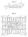
- Fig. 3 illustrates electrical connector 30 having a connector body 31 and a mating pin 32.
- the connector body 31 and the pin 32 are made of high conductivity metal such as copper-nickel-tin alloy No. 725 (88.2 wt % Cu, 9.5 Ni, 2.3 Sn; ASTM Spec. No. B122), and the pin and body serve as exemplary substrates for this process.
- the next step, shown in Block B, is to coat the conductive substrate with an amorphous coating such as a nickel-phosphorus coating.
- the amorphous layer should have a thickness greater than about 0.1 ⁇ m and is preferably about 0.5 to 1.0 ⁇ m. It can be electrodeposited Ni-P with P content higher than about 10 wt % to assure amorphous structure.
- a suitable Ni-P amorphous layer can be electrodeposited using the following bath composition: Nickel sulfate NiSO 4 6H 2 O 100 - 300 g/l Nickel chloride NiCl 2 6H 2 O 40 - 60 g/l Phosphorous acid H 3 PO 3 40 - 100 g/l Phosphoric acid H 3 PO 4 0 - 50 g/l
- the third step, Block C, is to apply over the amorphous coating a middle layer of corrosion resistant metal such as nickel.
- the metal middle layer should have a thickness greater than about 0.1 ⁇ m and is preferably about 0.5-1.0 ⁇ m.
- a suitable Ni layer can be electrodeposited using the following bath: Nickel sulfamate Ni(SO 3 NH 2 ) 2 4H 2 O 315 - 650 g/l Nickel chloride NiCl 2 6H 2 O 0 - 22 g/l Boric acid H 3 BO 3 30 - 45 g/l
- a wetting agent to avoid pits in deposit and a hardening agent to increase hardness of deposit may be added to the bath based on requirements.
- the metal middle coating can be a nickel alloy, cobalt or a cobalt alloy.
- the next step, shown in Block D, is to apply one or more layers of precious metal (palladium, gold, rhodium, ruthenium, platinum or their alloys such as palladium-nickel or palladium-cobalt) on top of the middle layer.
- the precious metal total thickness is less than about 1.5 ⁇ m.
- For a connector it is advantageously greater than about 0.1 ⁇ m and preferably about 0.5-1.0 ⁇ m.
- a suitable palladium layer can be deposited from the palladium electroplating solution described in United States Patent No. 4,911,799 issued on March 27, 1990 to J.A. Abys et al., which is incorporated herein by reference.
- a palladium-nickel alloy with nickel content preferably 10-30 wt % can be deposited from the electroplating solution described in United States Patent No. 4,911,798 issued on March 27, 1990 to J.A. Abys et al., which is incorporated herein by reference.
- a palladium-cobalt alloy can be deposited as described in the copending United States Patent application S.N. 08/974,120, filed by J.A. Abys et al. on November 19, 1997 which is incorporated herein by reference.
- Exemplary compositions and electroplating conditions for depositing gold layers are described in F.H. Reed et al., Gold Plating Technology , pp. 26 and 46 (Electrochemical Publications Ltd., Scotland, 1987). Plating of rhodium, ruthenium and platinum are described in Metal Finishing , (Guidebook and Directory Issue), Vol. 97, No. 1 (January, 1999).
- Figs. 4A and 4B show finished Cu substrates sequentially subjected to H 2 SO 3 (24 hrs), to (NH 4 ) 2 S(15 mins) and to heat at 75° C (15 min). Black spots indicate corrosion caused by porosity in the finish.
- Photograph Fig. 4A shows the conventional finish.
- Photograph 4B shows the finish described herein. As can be seen, the inventive finish exhibits less corrosion.
- An integrated circuit lead frame can also be fabricated by the process illustrated in Fig. 2. The only differences are that the substrate is different and the precious metal thickness can be less ( ⁇ 0.025 ⁇ m).
- Fig. 5 illustrates a substrate 50 formed into configuration for use as a lead frame for an integrated circuit (IC).
- the substrate 50 includes a paddle 52 on which the IC is to be mounted and the leads 53 on which the IC is to be bonded.
- Dam bars 54 interconnect the leads before packaging. After the integrated circuit is bonded and a packaging medium has been applied over an area shown in phantom lines 55, the dam bars 54 are trimmed away.
- the substrate of the lead frame can be copper or a copper alloy such as alloy No. 151 (99.9 wt.% Cu, 0.1% Zr) or alloy No. 194 (97.5 wt.% Cu, 2.35% Fe, 0.03% P, 0.12% Zn).
- Other conductive metals and alloys such as alloy No. 42 (42 wt. % Ni, 58% Fe) can also be used.
- an integrated circuit 56 is mounted and bonded to the coated substrate as described in United States Patent No. 5,675,177 issued October 7, 1997 to J.A. Abys et al.
- This surface finish is that it is much less porous than the conventional nickel/precious metal finish and is an efficient barrier to reduce exposure of the substrate metal.
Landscapes
- Chemical & Material Sciences (AREA)
- Engineering & Computer Science (AREA)
- Chemical Kinetics & Catalysis (AREA)
- Materials Engineering (AREA)
- Metallurgy (AREA)
- Organic Chemistry (AREA)
- Electrochemistry (AREA)
- Crystallography & Structural Chemistry (AREA)
- Physics & Mathematics (AREA)
- Thermal Sciences (AREA)
- General Chemical & Material Sciences (AREA)
- Mechanical Engineering (AREA)
- Electroplating Methods And Accessories (AREA)
- Parts Printed On Printed Circuit Boards (AREA)
- Non-Insulated Conductors (AREA)
- Lead Frames For Integrated Circuits (AREA)
Abstract
Description
| Nickel sulfate | NiSO46H2O | 100 - 300 g/l |
| Nickel chloride | NiCl26H2O | 40 - 60 g/l |
| Phosphorous acid | H3PO3 | 40 - 100 g/l |
| Phosphoric acid | H3PO4 | 0 - 50 g/l |
| Nickel sulfamate | Ni(SO3NH2)24H2O | 315 - 650 g/l |
| Nickel chloride | NiCl26H2O | 0 - 22 g/l |
| Boric acid | H3BO3 | 30 - 45 g/l |
Claims (8)
- A coated metal article comprising:a metal substrate;disposed on the substrate a multilayer surface finish comprising, in succession, an amorphous metal underlayer, a metal middle layer and at least one outer layer comprising precious metal.
- The article of claim 1 wherein the amorphous metal is selected from the group consisting of nickel-phosphorus, nickel-phosphorus-tungsten and cobalt-phosphorus.
- The article of claim 1 wherein the middle metal layer comprises a metal selected from the group consisting of nickel, nickel alloy, cobalt and cobalt alloy.
- The article of claim 1 wherein the precious metal comprises a metal selected from the group consisting of palladium, gold, rhodium, ruthenium and platinum.
- The article of claim 1 wherein the metal substrate comprises copper, iron or nickel.
- The article of claim 1 wherein the amorphous metal has a thickness in the range 0.1 - 2.5 µm, the metal middle layer has a thickness in the range 0.1 - 2.5 µm and the precious metal has a thickness less than 1.5 µm.
- An electrical connector comprising a coated article in accordance with claim 1.
- A lead frame for an integrated circuit comprising a coated article in accordance with claim 1.
Applications Claiming Priority (2)
| Application Number | Priority Date | Filing Date | Title |
|---|---|---|---|
| US09/404,059 US6335107B1 (en) | 1999-09-23 | 1999-09-23 | Metal article coated with multilayer surface finish for porosity reduction |
| US404059 | 1999-09-23 |
Publications (3)
| Publication Number | Publication Date |
|---|---|
| EP1086807A2 true EP1086807A2 (en) | 2001-03-28 |
| EP1086807A3 EP1086807A3 (en) | 2001-10-31 |
| EP1086807B1 EP1086807B1 (en) | 2004-11-10 |
Family
ID=23597974
Family Applications (1)
| Application Number | Title | Priority Date | Filing Date |
|---|---|---|---|
| EP00307862A Expired - Lifetime EP1086807B1 (en) | 1999-09-23 | 2000-09-11 | Metal article coated with multilayer surface finish for porosity reduction |
Country Status (7)
| Country | Link |
|---|---|
| US (1) | US6335107B1 (en) |
| EP (1) | EP1086807B1 (en) |
| JP (1) | JP2001152385A (en) |
| KR (1) | KR100783847B1 (en) |
| DE (1) | DE60015686T2 (en) |
| MY (1) | MY135997A (en) |
| SG (1) | SG87169A1 (en) |
Cited By (5)
| Publication number | Priority date | Publication date | Assignee | Title |
|---|---|---|---|---|
| EP1444528A4 (en) * | 2001-09-24 | 2005-12-28 | Rika Electronics Internat | Electrical test probes and methods of making the same |
| WO2011005302A1 (en) * | 2009-07-10 | 2011-01-13 | Xtalic Corporation | Coated articles and methods |
| WO2015154807A1 (en) * | 2014-04-10 | 2015-10-15 | Kromberg & Schubert Gmbh | Metal component, and method for producing a metal component |
| ITUA20162707A1 (en) * | 2016-04-19 | 2017-10-19 | Bluclad S R L | Phosphorus-Cobalt-Nickel alloy and its use in the processes of plating with noble metals of non-noble metal objects. |
| CN111926354A (en) * | 2020-10-12 | 2020-11-13 | 江西科技学院 | Electric element for computer data processing device and manufacturing method thereof |
Families Citing this family (26)
| Publication number | Priority date | Publication date | Assignee | Title |
|---|---|---|---|---|
| JP3519727B1 (en) | 2002-12-09 | 2004-04-19 | Fcm株式会社 | Connector terminal and connector having the same |
| JP3519726B1 (en) | 2002-11-26 | 2004-04-19 | Fcm株式会社 | Terminal and parts having it |
| JP3442764B1 (en) | 2002-08-22 | 2003-09-02 | エフシーエム株式会社 | Connector terminals and connectors |
| US6984358B2 (en) * | 2002-09-13 | 2006-01-10 | Lockheed Martin Corporation | Diffusion bonding process of two-phase metal alloys |
| JP3519731B1 (en) | 2003-07-29 | 2004-04-19 | Fcm株式会社 | Terminals, parts and products having them |
| JP3985788B2 (en) * | 2004-01-22 | 2007-10-03 | セイコーエプソン株式会社 | Electro-optical device and electronic apparatus |
| US7297397B2 (en) | 2004-07-26 | 2007-11-20 | Npa Coatings, Inc. | Method for applying a decorative metal layer |
| US7215014B2 (en) * | 2004-07-29 | 2007-05-08 | Freescale Semiconductor, Inc. | Solderable metal finish for integrated circuit package leads and method for forming |
| DE102004047522B3 (en) * | 2004-09-28 | 2006-04-06 | Infineon Technologies Ag | Semiconductor chip having a metal coating structure and method of making the same |
| DE102006018765A1 (en) * | 2006-04-20 | 2007-10-25 | Infineon Technologies Ag | Power semiconductor component, power semiconductor component and method for its production |
| US7521128B2 (en) * | 2006-05-18 | 2009-04-21 | Xtalic Corporation | Methods for the implementation of nanocrystalline and amorphous metals and alloys as coatings |
| WO2013094766A1 (en) * | 2011-12-22 | 2013-06-27 | オーエム産業株式会社 | Plated article and manufacturing method therefor |
| JP5991712B2 (en) * | 2012-10-26 | 2016-09-14 | Shマテリアル株式会社 | Semiconductor device mounting substrate and manufacturing method thereof |
| JP6057285B2 (en) * | 2012-10-26 | 2017-01-11 | Shマテリアル株式会社 | Semiconductor device mounting substrate |
| JP6085536B2 (en) * | 2013-08-05 | 2017-02-22 | 株式会社Shカッパープロダクツ | Copper strip, plated copper strip, lead frame and LED module |
| JP6181581B2 (en) * | 2014-03-10 | 2017-08-16 | トヨタ自動車株式会社 | Terminal connection structure, semiconductor device |
| US9070392B1 (en) | 2014-12-16 | 2015-06-30 | Hutchinson Technology Incorporated | Piezoelectric disk drive suspension motors having plated stiffeners |
| WO2017003782A1 (en) | 2015-06-30 | 2017-01-05 | Hutchinson Technology Incorporated | Disk drive head suspension structures having improved gold-dielectric joint reliability |
| DE202017001425U1 (en) | 2016-03-18 | 2017-07-06 | Apple Inc. | Contacts made of precious metal alloys |
| US10998657B2 (en) | 2016-03-18 | 2021-05-04 | Apple Inc. | Precious-metal-alloy contacts |
| KR101723975B1 (en) * | 2016-12-15 | 2017-04-07 | 주식회사 제이미크론 | Charger Terminals for Waterproofing of Cellular Phone and Manufacturing Method of it |
| DE102017002472A1 (en) * | 2017-03-14 | 2018-09-20 | Diehl Metal Applications Gmbh | Connectors |
| US20190103693A1 (en) * | 2017-09-29 | 2019-04-04 | Apple Inc. | Electrical contacts having sacrificial layer for corrosion protection |
| KR102148316B1 (en) * | 2018-12-11 | 2020-08-26 | 히로세코리아 주식회사 | Electrical contact terminal |
| JP7231720B2 (en) * | 2019-04-22 | 2023-03-01 | Ngkエレクトロデバイス株式会社 | Packages and metal frames for packages |
| JP2022105401A (en) * | 2021-01-04 | 2022-07-14 | 株式会社東芝 | Connector, contact pin connection method, contact pin, and storage medium |
Family Cites Families (11)
| Publication number | Priority date | Publication date | Assignee | Title |
|---|---|---|---|---|
| US3617320A (en) | 1968-08-06 | 1971-11-02 | Hooker Chemical Corp | Metallizing substrates |
| DE1804152A1 (en) * | 1968-10-19 | 1970-04-30 | Telefunken Patent | Ferromagnetic nickel iron alloy |
| GB2129441B (en) * | 1982-11-05 | 1985-12-11 | Standard Telephones Cables Ltd | Gold plating |
| ATE40721T1 (en) * | 1984-05-11 | 1989-02-15 | Burlington Industries Inc | ELECTRICAL CONTACT COATED WITH AN AMORPHOUS TRANSITION ALLOY WHICH IS ITSELF COATED WITH A GOLD FILM. |
| US4808967A (en) | 1985-05-29 | 1989-02-28 | Ohmega Electronics | Circuit board material |
| JPH01132072A (en) * | 1987-11-18 | 1989-05-24 | Yazaki Corp | Gold plated parts of terminal, contact, and the like |
| JPH0359972A (en) * | 1989-07-27 | 1991-03-14 | Yazaki Corp | Electrical contact |
| US5180482A (en) | 1991-07-22 | 1993-01-19 | At&T Bell Laboratories | Thermal annealing of palladium alloys |
| US5631094A (en) * | 1994-01-28 | 1997-05-20 | Komag, Incorporated | Magnetic alloy for improved corrosion resistance and magnetic performance |
| US5675177A (en) | 1995-06-26 | 1997-10-07 | Lucent Technologies Inc. | Ultra-thin noble metal coatings for electronic packaging |
| US6139977A (en) * | 1998-06-10 | 2000-10-31 | Lucent Technologies Inc. | Palladium surface coating suitable for wirebonding and process for forming palladium surface coatings |
-
1999
- 1999-09-23 US US09/404,059 patent/US6335107B1/en not_active Expired - Lifetime
-
2000
- 2000-09-11 EP EP00307862A patent/EP1086807B1/en not_active Expired - Lifetime
- 2000-09-11 DE DE60015686T patent/DE60015686T2/en not_active Expired - Lifetime
- 2000-09-19 SG SG200005261A patent/SG87169A1/en unknown
- 2000-09-21 MY MYPI20004397A patent/MY135997A/en unknown
- 2000-09-21 JP JP2000286389A patent/JP2001152385A/en active Pending
- 2000-09-22 KR KR1020000055641A patent/KR100783847B1/en not_active Expired - Fee Related
Cited By (9)
| Publication number | Priority date | Publication date | Assignee | Title |
|---|---|---|---|---|
| EP1444528A4 (en) * | 2001-09-24 | 2005-12-28 | Rika Electronics Internat | Electrical test probes and methods of making the same |
| WO2011005302A1 (en) * | 2009-07-10 | 2011-01-13 | Xtalic Corporation | Coated articles and methods |
| US8652649B2 (en) | 2009-07-10 | 2014-02-18 | Xtalic Corporation | Coated articles and methods |
| US9074294B2 (en) | 2009-07-10 | 2015-07-07 | Xtalic Corporation | Coated articles and methods |
| US9765438B2 (en) | 2009-07-10 | 2017-09-19 | Xtalic Corporation | Coated articles and methods |
| WO2015154807A1 (en) * | 2014-04-10 | 2015-10-15 | Kromberg & Schubert Gmbh | Metal component, and method for producing a metal component |
| ITUA20162707A1 (en) * | 2016-04-19 | 2017-10-19 | Bluclad S R L | Phosphorus-Cobalt-Nickel alloy and its use in the processes of plating with noble metals of non-noble metal objects. |
| WO2017182957A1 (en) * | 2016-04-19 | 2017-10-26 | Bluclad S.R.L. | Phosphorous-cobalt-nickel alloy and use thereof in plating processes of non-precious metal objects with precious metals |
| CN111926354A (en) * | 2020-10-12 | 2020-11-13 | 江西科技学院 | Electric element for computer data processing device and manufacturing method thereof |
Also Published As
| Publication number | Publication date |
|---|---|
| SG87169A1 (en) | 2002-03-19 |
| KR20010050575A (en) | 2001-06-15 |
| EP1086807A3 (en) | 2001-10-31 |
| MY135997A (en) | 2008-07-31 |
| HK1032562A1 (en) | 2001-07-27 |
| KR100783847B1 (en) | 2007-12-10 |
| EP1086807B1 (en) | 2004-11-10 |
| JP2001152385A (en) | 2001-06-05 |
| DE60015686D1 (en) | 2004-12-16 |
| DE60015686T2 (en) | 2005-12-01 |
| US6335107B1 (en) | 2002-01-01 |
Similar Documents
| Publication | Publication Date | Title |
|---|---|---|
| EP1086807B1 (en) | Metal article coated with multilayer surface finish for porosity reduction | |
| EP1257004B1 (en) | Metal article with multilayer coating | |
| EP1256981A1 (en) | Metal article coated with near-surface doped tin or tin alloy | |
| EP1352993B1 (en) | A method for preparation of metal-plated material | |
| US7808109B2 (en) | Fretting and whisker resistant coating system and method | |
| JP3880877B2 (en) | Plated copper or copper alloy and method for producing the same | |
| CN100528550C (en) | Heat-resistant protective film, method for producing same, and electrical and electronic component | |
| CN101981235A (en) | Connecting component metal material and manufacturing method thereof | |
| JP2726434B2 (en) | Sn or Sn alloy coating material | |
| US6090263A (en) | Process for coating an article with a conformable nickel coating | |
| JPH11222659A (en) | Process for producing metal composite strip | |
| US20050249969A1 (en) | Preserving solderability and inhibiting whisker growth in tin surfaces of electronic components | |
| US20050249968A1 (en) | Whisker inhibition in tin surfaces of electronic components | |
| US20080261071A1 (en) | Preserving Solderability and Inhibiting Whisker Growth in Tin Surfaces of Electronic Components | |
| US4895771A (en) | Electrical contact surface coating | |
| GB2186597A (en) | Electrical contact surface coating | |
| HK1032562B (en) | Metal article coated with multilayer surface finish for porosity reduction | |
| JPH043041B2 (en) | ||
| EP0531099A2 (en) | Corrosion resistant high temperature contacts or electrical connectors and method of fabrication thereof | |
| CN103317790A (en) | Multilayer matte tin plated film and preparation method thereof | |
| JP3066952B2 (en) | Lead frame material | |
| JPS60217693A (en) | Lead wire for electronic part | |
| JPH06340981A (en) | Alloy film and method for producing the same | |
| JPS6153434B2 (en) | ||
| HK1118950B (en) | Fretting and whisker resistant coating system and method |
Legal Events
| Date | Code | Title | Description |
|---|---|---|---|
| PUAI | Public reference made under article 153(3) epc to a published international application that has entered the european phase |
Free format text: ORIGINAL CODE: 0009012 |
|
| AK | Designated contracting states |
Kind code of ref document: A2 Designated state(s): DE GB Kind code of ref document: A2 Designated state(s): AT BE CH CY DE DK ES FI FR GB GR IE IT LI LU MC NL PT SE |
|
| AX | Request for extension of the european patent |
Free format text: AL;LT;LV;MK;RO;SI |
|
| PUAL | Search report despatched |
Free format text: ORIGINAL CODE: 0009013 |
|
| AK | Designated contracting states |
Kind code of ref document: A3 Designated state(s): AT BE CH CY DE DK ES FI FR GB GR IE IT LI LU MC NL PT SE |
|
| AX | Request for extension of the european patent |
Free format text: AL;LT;LV;MK;RO;SI |
|
| RIC1 | Information provided on ipc code assigned before grant |
Free format text: 7B 32B 15/01 A, 7C 25D 3/56 B, 7H 01H 1/02 B, 7H 01R 13/03 B |
|
| 17P | Request for examination filed |
Effective date: 20020420 |
|
| AKX | Designation fees paid |
Free format text: DE GB |
|
| 17Q | First examination report despatched |
Effective date: 20030325 |
|
| GRAP | Despatch of communication of intention to grant a patent |
Free format text: ORIGINAL CODE: EPIDOSNIGR1 |
|
| GRAS | Grant fee paid |
Free format text: ORIGINAL CODE: EPIDOSNIGR3 |
|
| GRAA | (expected) grant |
Free format text: ORIGINAL CODE: 0009210 |
|
| AK | Designated contracting states |
Kind code of ref document: B1 Designated state(s): DE GB |
|
| REG | Reference to a national code |
Ref country code: GB Ref legal event code: FG4D |
|
| REF | Corresponds to: |
Ref document number: 60015686 Country of ref document: DE Date of ref document: 20041216 Kind code of ref document: P |
|
| REG | Reference to a national code |
Ref country code: HK Ref legal event code: GR Ref document number: 1032562 Country of ref document: HK |
|
| PLBE | No opposition filed within time limit |
Free format text: ORIGINAL CODE: 0009261 |
|
| STAA | Information on the status of an ep patent application or granted ep patent |
Free format text: STATUS: NO OPPOSITION FILED WITHIN TIME LIMIT |
|
| 26N | No opposition filed |
Effective date: 20050811 |
|
| REG | Reference to a national code |
Ref country code: GB Ref legal event code: 732E Free format text: REGISTERED BETWEEN 20131107 AND 20131113 |
|
| PGFP | Annual fee paid to national office [announced via postgrant information from national office to epo] |
Ref country code: DE Payment date: 20160921 Year of fee payment: 17 Ref country code: GB Payment date: 20160920 Year of fee payment: 17 |
|
| REG | Reference to a national code |
Ref country code: DE Ref legal event code: R119 Ref document number: 60015686 Country of ref document: DE |
|
| GBPC | Gb: european patent ceased through non-payment of renewal fee |
Effective date: 20170911 |
|
| PG25 | Lapsed in a contracting state [announced via postgrant information from national office to epo] |
Ref country code: DE Free format text: LAPSE BECAUSE OF NON-PAYMENT OF DUE FEES Effective date: 20180404 Ref country code: GB Free format text: LAPSE BECAUSE OF NON-PAYMENT OF DUE FEES Effective date: 20170911 |
|
| REG | Reference to a national code |
Ref country code: DE Ref legal event code: R081 Ref document number: 60015686 Country of ref document: DE Owner name: WSOU INVESTMENTS, LLC, LOS ANGELES, US Free format text: FORMER OWNER: LUCENT TECHNOLOGIES INC., MURRAY HILL, N.J., US |