EP1085789A2 - Method of fabricating a laminated circuit assembly and product thereof - Google Patents
Method of fabricating a laminated circuit assembly and product thereof Download PDFInfo
- Publication number
- EP1085789A2 EP1085789A2 EP00119863A EP00119863A EP1085789A2 EP 1085789 A2 EP1085789 A2 EP 1085789A2 EP 00119863 A EP00119863 A EP 00119863A EP 00119863 A EP00119863 A EP 00119863A EP 1085789 A2 EP1085789 A2 EP 1085789A2
- Authority
- EP
- European Patent Office
- Prior art keywords
- sheet
- slit
- circuit
- circuit sheet
- backing sheet
- Prior art date
- Legal status (The legal status is an assumption and is not a legal conclusion. Google has not performed a legal analysis and makes no representation as to the accuracy of the status listed.)
- Withdrawn
Links
- 238000004519 manufacturing process Methods 0.000 title claims abstract description 10
- 239000000758 substrate Substances 0.000 claims abstract description 31
- 230000002093 peripheral effect Effects 0.000 claims abstract description 25
- 238000000034 method Methods 0.000 claims description 16
- 125000006850 spacer group Chemical group 0.000 claims description 12
- 239000000463 material Substances 0.000 claims description 11
- 239000000853 adhesive Substances 0.000 claims description 6
- 230000001070 adhesive effect Effects 0.000 claims description 6
- 238000005520 cutting process Methods 0.000 claims description 6
- 238000000151 deposition Methods 0.000 claims 1
- 239000010410 layer Substances 0.000 description 11
- 239000012528 membrane Substances 0.000 description 7
- 230000000712 assembly Effects 0.000 description 5
- 238000000429 assembly Methods 0.000 description 5
- 239000012790 adhesive layer Substances 0.000 description 2
- 239000002313 adhesive film Substances 0.000 description 1
- 230000015572 biosynthetic process Effects 0.000 description 1
- 239000004020 conductor Substances 0.000 description 1
- 230000000994 depressogenic effect Effects 0.000 description 1
- 238000005304 joining Methods 0.000 description 1
- 238000009877 rendering Methods 0.000 description 1
Images




Classifications
-
- H—ELECTRICITY
- H05—ELECTRIC TECHNIQUES NOT OTHERWISE PROVIDED FOR
- H05K—PRINTED CIRCUITS; CASINGS OR CONSTRUCTIONAL DETAILS OF ELECTRIC APPARATUS; MANUFACTURE OF ASSEMBLAGES OF ELECTRICAL COMPONENTS
- H05K3/00—Apparatus or processes for manufacturing printed circuits
- H05K3/0058—Laminating printed circuit boards onto other substrates, e.g. metallic substrates
-
- H—ELECTRICITY
- H05—ELECTRIC TECHNIQUES NOT OTHERWISE PROVIDED FOR
- H05K—PRINTED CIRCUITS; CASINGS OR CONSTRUCTIONAL DETAILS OF ELECTRIC APPARATUS; MANUFACTURE OF ASSEMBLAGES OF ELECTRICAL COMPONENTS
- H05K2201/00—Indexing scheme relating to printed circuits covered by H05K1/00
- H05K2201/09—Shape and layout
- H05K2201/09009—Substrate related
- H05K2201/0909—Preformed cutting or breaking line
-
- H—ELECTRICITY
- H05—ELECTRIC TECHNIQUES NOT OTHERWISE PROVIDED FOR
- H05K—PRINTED CIRCUITS; CASINGS OR CONSTRUCTIONAL DETAILS OF ELECTRIC APPARATUS; MANUFACTURE OF ASSEMBLAGES OF ELECTRICAL COMPONENTS
- H05K2201/00—Indexing scheme relating to printed circuits covered by H05K1/00
- H05K2201/20—Details of printed circuits not provided for in H05K2201/01 - H05K2201/10
- H05K2201/2009—Reinforced areas, e.g. for a specific part of a flexible printed circuit
-
- H—ELECTRICITY
- H05—ELECTRIC TECHNIQUES NOT OTHERWISE PROVIDED FOR
- H05K—PRINTED CIRCUITS; CASINGS OR CONSTRUCTIONAL DETAILS OF ELECTRIC APPARATUS; MANUFACTURE OF ASSEMBLAGES OF ELECTRICAL COMPONENTS
- H05K2203/00—Indexing scheme relating to apparatus or processes for manufacturing printed circuits covered by H05K3/00
- H05K2203/02—Details related to mechanical or acoustic processing, e.g. drilling, punching, cutting, using ultrasound
- H05K2203/0264—Peeling insulating layer, e.g. foil, or separating mask
-
- H—ELECTRICITY
- H05—ELECTRIC TECHNIQUES NOT OTHERWISE PROVIDED FOR
- H05K—PRINTED CIRCUITS; CASINGS OR CONSTRUCTIONAL DETAILS OF ELECTRIC APPARATUS; MANUFACTURE OF ASSEMBLAGES OF ELECTRICAL COMPONENTS
- H05K2203/00—Indexing scheme relating to apparatus or processes for manufacturing printed circuits covered by H05K3/00
- H05K2203/06—Lamination
- H05K2203/066—Transfer laminating of insulating material, e.g. resist as a whole layer, not as a pattern
-
- H—ELECTRICITY
- H05—ELECTRIC TECHNIQUES NOT OTHERWISE PROVIDED FOR
- H05K—PRINTED CIRCUITS; CASINGS OR CONSTRUCTIONAL DETAILS OF ELECTRIC APPARATUS; MANUFACTURE OF ASSEMBLAGES OF ELECTRICAL COMPONENTS
- H05K3/00—Apparatus or processes for manufacturing printed circuits
- H05K3/38—Improvement of the adhesion between the insulating substrate and the metal
- H05K3/386—Improvement of the adhesion between the insulating substrate and the metal by the use of an organic polymeric bonding layer, e.g. adhesive
-
- Y—GENERAL TAGGING OF NEW TECHNOLOGICAL DEVELOPMENTS; GENERAL TAGGING OF CROSS-SECTIONAL TECHNOLOGIES SPANNING OVER SEVERAL SECTIONS OF THE IPC; TECHNICAL SUBJECTS COVERED BY FORMER USPC CROSS-REFERENCE ART COLLECTIONS [XRACs] AND DIGESTS
- Y10—TECHNICAL SUBJECTS COVERED BY FORMER USPC
- Y10T—TECHNICAL SUBJECTS COVERED BY FORMER US CLASSIFICATION
- Y10T156/00—Adhesive bonding and miscellaneous chemical manufacture
- Y10T156/10—Methods of surface bonding and/or assembly therefor
- Y10T156/1052—Methods of surface bonding and/or assembly therefor with cutting, punching, tearing or severing
-
- Y—GENERAL TAGGING OF NEW TECHNOLOGICAL DEVELOPMENTS; GENERAL TAGGING OF CROSS-SECTIONAL TECHNOLOGIES SPANNING OVER SEVERAL SECTIONS OF THE IPC; TECHNICAL SUBJECTS COVERED BY FORMER USPC CROSS-REFERENCE ART COLLECTIONS [XRACs] AND DIGESTS
- Y10—TECHNICAL SUBJECTS COVERED BY FORMER USPC
- Y10T—TECHNICAL SUBJECTS COVERED BY FORMER US CLASSIFICATION
- Y10T156/00—Adhesive bonding and miscellaneous chemical manufacture
- Y10T156/10—Methods of surface bonding and/or assembly therefor
- Y10T156/1052—Methods of surface bonding and/or assembly therefor with cutting, punching, tearing or severing
- Y10T156/1056—Perforating lamina
-
- Y—GENERAL TAGGING OF NEW TECHNOLOGICAL DEVELOPMENTS; GENERAL TAGGING OF CROSS-SECTIONAL TECHNOLOGIES SPANNING OVER SEVERAL SECTIONS OF THE IPC; TECHNICAL SUBJECTS COVERED BY FORMER USPC CROSS-REFERENCE ART COLLECTIONS [XRACs] AND DIGESTS
- Y10—TECHNICAL SUBJECTS COVERED BY FORMER USPC
- Y10T—TECHNICAL SUBJECTS COVERED BY FORMER US CLASSIFICATION
- Y10T156/00—Adhesive bonding and miscellaneous chemical manufacture
- Y10T156/10—Methods of surface bonding and/or assembly therefor
- Y10T156/1052—Methods of surface bonding and/or assembly therefor with cutting, punching, tearing or severing
- Y10T156/1056—Perforating lamina
- Y10T156/1057—Subsequent to assembly of laminae
-
- Y—GENERAL TAGGING OF NEW TECHNOLOGICAL DEVELOPMENTS; GENERAL TAGGING OF CROSS-SECTIONAL TECHNOLOGIES SPANNING OVER SEVERAL SECTIONS OF THE IPC; TECHNICAL SUBJECTS COVERED BY FORMER USPC CROSS-REFERENCE ART COLLECTIONS [XRACs] AND DIGESTS
- Y10—TECHNICAL SUBJECTS COVERED BY FORMER USPC
- Y10T—TECHNICAL SUBJECTS COVERED BY FORMER US CLASSIFICATION
- Y10T156/00—Adhesive bonding and miscellaneous chemical manufacture
- Y10T156/10—Methods of surface bonding and/or assembly therefor
- Y10T156/1052—Methods of surface bonding and/or assembly therefor with cutting, punching, tearing or severing
- Y10T156/1062—Prior to assembly
-
- Y—GENERAL TAGGING OF NEW TECHNOLOGICAL DEVELOPMENTS; GENERAL TAGGING OF CROSS-SECTIONAL TECHNOLOGIES SPANNING OVER SEVERAL SECTIONS OF THE IPC; TECHNICAL SUBJECTS COVERED BY FORMER USPC CROSS-REFERENCE ART COLLECTIONS [XRACs] AND DIGESTS
- Y10—TECHNICAL SUBJECTS COVERED BY FORMER USPC
- Y10T—TECHNICAL SUBJECTS COVERED BY FORMER US CLASSIFICATION
- Y10T156/00—Adhesive bonding and miscellaneous chemical manufacture
- Y10T156/10—Methods of surface bonding and/or assembly therefor
- Y10T156/1052—Methods of surface bonding and/or assembly therefor with cutting, punching, tearing or severing
- Y10T156/1062—Prior to assembly
- Y10T156/1074—Separate cutting of separate sheets or webs
-
- Y—GENERAL TAGGING OF NEW TECHNOLOGICAL DEVELOPMENTS; GENERAL TAGGING OF CROSS-SECTIONAL TECHNOLOGIES SPANNING OVER SEVERAL SECTIONS OF THE IPC; TECHNICAL SUBJECTS COVERED BY FORMER USPC CROSS-REFERENCE ART COLLECTIONS [XRACs] AND DIGESTS
- Y10—TECHNICAL SUBJECTS COVERED BY FORMER USPC
- Y10T—TECHNICAL SUBJECTS COVERED BY FORMER US CLASSIFICATION
- Y10T428/00—Stock material or miscellaneous articles
- Y10T428/15—Sheet, web, or layer weakened to permit separation through thickness
-
- Y—GENERAL TAGGING OF NEW TECHNOLOGICAL DEVELOPMENTS; GENERAL TAGGING OF CROSS-SECTIONAL TECHNOLOGIES SPANNING OVER SEVERAL SECTIONS OF THE IPC; TECHNICAL SUBJECTS COVERED BY FORMER USPC CROSS-REFERENCE ART COLLECTIONS [XRACs] AND DIGESTS
- Y10—TECHNICAL SUBJECTS COVERED BY FORMER USPC
- Y10T—TECHNICAL SUBJECTS COVERED BY FORMER US CLASSIFICATION
- Y10T428/00—Stock material or miscellaneous articles
- Y10T428/24—Structurally defined web or sheet [e.g., overall dimension, etc.]
- Y10T428/24273—Structurally defined web or sheet [e.g., overall dimension, etc.] including aperture
- Y10T428/24298—Noncircular aperture [e.g., slit, diamond, rectangular, etc.]
- Y10T428/24314—Slit or elongated
-
- Y—GENERAL TAGGING OF NEW TECHNOLOGICAL DEVELOPMENTS; GENERAL TAGGING OF CROSS-SECTIONAL TECHNOLOGIES SPANNING OVER SEVERAL SECTIONS OF THE IPC; TECHNICAL SUBJECTS COVERED BY FORMER USPC CROSS-REFERENCE ART COLLECTIONS [XRACs] AND DIGESTS
- Y10—TECHNICAL SUBJECTS COVERED BY FORMER USPC
- Y10T—TECHNICAL SUBJECTS COVERED BY FORMER US CLASSIFICATION
- Y10T428/00—Stock material or miscellaneous articles
- Y10T428/24—Structurally defined web or sheet [e.g., overall dimension, etc.]
- Y10T428/24777—Edge feature
Definitions
- This invention generally relates to the art of electrical circuitry and, particularly, to a method of fabricating a laminated circuit assembly, such as an assembly for adhering to the face of a control panel of an electrical appliance.
- Laminated circuit assemblies are used in a wide variety of applications. For instance, such circuit assemblies are used in laminated electrical switches which sometimes are called membrane or "touch" switches.
- a membrane switch may include an insulative substrate or circuit sheet, such as of plastic material, which mounts or supports thin conductive contacts, such as printed circuitry.
- a flexible membrane is laminated to the substrate.
- a spacer layer often is sandwiched between the membrane and the substrate, with an aperture in the spacer layer aligned with the contacts. When the flexible membrane is depressed in the area of the aperture in the spacer layer, it flexes such that a contact on the membrane engages the contacts on the substrate to dose the switch.
- Laminated circuit assemblies such as laminated electrical switches as described above, often are adhered to the face of a control panel of an electrical appliance, such as household appliances.
- the back side of a substrate or circuit sheet has an adhesive film applied thereto, and a flexible backing sheet is adhered to the adhesive.
- the backing sheet is stripped from the substrate to expose the adhesive on the back side of the substrate.
- a pull tab is formed out of the substrate and remains adhered to the flexible backing sheet so that the backing sheet can be easily grasped and stripped. Problems often are encountered in forming the pull tab from the substrate so that the pull tab is easily separated from the substrate to facilitate stripping the flexible backing sheet.
- the various sheets or layers of the laminated circuit assembly are cut to their desired shapes or configurations in stamping-type cutting operations.
- a cut or slit must be stamped which will define and separate the pull tab from the substrate. This cut must not cut through the backing sheet or else the pull tab would separate from the backing sheet when pulled, rendering the pull tab useless for the purpose of stripping the backing sheet from the substrate.
- Positioning the cutting blade such that it will reliably cut completely through the substrate but not through the backing sheet is very difficult. This difficulty can result in the production of many assemblies that are out of specification, thereby increasing scrap cost.
- the present invention is directed to solving these problems.
- An object, therefore, of the invention is to provide a new and improved method of fabricating a laminated circuit assembly of the character described.
- Another object of the invention is to provide a method of fabricating a laminated circuit assembly for adhering to the face of a control panel of an electrical appliance, for instance.
- the method includes the steps of providing a plastic circuit sheet with electrical circuitry printed thereon.
- a slit is cut in the circuit sheet in an area where a pull tab subsequently is to be located.
- An adhesive is deposited on a back side of the circuit sheet, and a backing sheet is adhered thereto.
- the resulting laminated circuit sheet and backing sheet are cut with a peripheral cut around the circuitry.
- the peripheral cut intersects the slit with the cut forming a pull tab projecting outwardly from the slit. Therefore, the pull tab can be grasped and separated from the circuit sheet to strip the backing sheet from the circuit sheet when it is desired to adhere the circuit sheet to the face of the control panel.
- the slit is preferably U-shaped with the side legs of the U-shaped configuration defining spaced slit portions.
- the peripheral cut intersects the side legs of the U-shaped slit.
- the U-shaped slit is cut so that the side legs of the U-shaped configuration project outwardly.
- the backing sheet is provided of flexible material.
- the circuit sheet is of a material more rigid or stiff than the backing sheet.
- the invention is disclosed herein in a laminated electrical switch which includes a switch sheet adhered to the front side of the circuit sheet. A spacer layer is positioned between the switch sheet and the circuit sheet.
- the invention is embodied in a method of fabricating a laminated circuit assembly in the form of a laminated electrical switch assembly, generaily designated 10, which is adhered to the face of a control panel 12 of an electrical appliance, generaily designated 14.
- the appliance may be a dishwasher, a clothes washer, a clothes dryer or similar household appliance.
- the method of fabricating a laminated circuit assembly according to the invention is not limited to laminated electrical switch assemblies 10.
- Figures 2-8 represent various steps in the fabricating method of the invention. More particularly, Figure 2 shows a circuit sheet or substrate 16 of relatively stiff plastic material.
- the substrate has electrical circuitry, generaily designated 18, printed thereon.
- the term "printed" circuitry herein is meant in its broadest sense.
- Circuitry 18 can be applied to substrate 16 in a variety of processes other than literally printing the circuitry onto the substrate. In any event, the circuitry is formed by thin conductors including contact areas 20 and leads 22 which are connected to various operative components of appliance 14 whereby the circuitry can control operation of the appliance.
- a slit is cut or stamped in substrate 16 as seen in Figure 3.
- the slit is made in an area where a pull tab subsequently is to be located, as will be seen hereinafter.
- the slit 24 is preferably U-shaped to define a pair of spaced, parallel side legs or slits 24a joined by a cross slit 24b. Legs 24a project outwardly away from circuitry 18.
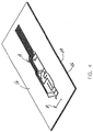
- Figure 4 shows the next step in the method of the invention, wherein an adhesive layer 26 is applied to a back side of circuit sheet 16 for subsequent adherence to the face of control panel 12 (Fig. 1).
- a backing sheet 28 is applied over adhesive layer 26 as sort of a "release sheet” to allow handling of the assembly prior to adherence to the appliance.
- the backing sheet also may be of plastic material, but of a relatively flexible material in comparison to circuit sheet 16 which is of a more rigid or stiff material.
- Figures 5 and 6 show the next step in the method of the invention whereby the now laminated circuit sheet 16 and backing sheet 28 are cut or stamped with a peripheral cut 30 defining a peripheral edge around circuitry 18 and in the final shape or configuration of the laminated circuit assembly. It should be noted that peripheral cut 30 intersects the slit 24. Peripheral cut 30 also is configured at 30a to define an outwardly projecting pull tab 32 cut completely thereabout and out of circuit sheet 16. Since slit 24 was made only in circuit sheet 16 and not backing sheet 28, pull tab 32 now has become separated from the circuit sheet and adhered to the backing sheet.
- the peripheral cut 30 intersects side legs 24a of the U-shaped slit 24. It should be understood that by having peripheral cut 30 intersect side legs or slit portions 24a of U-shaped slit 24, complete communication between the two cuts is easily achieved without much precision because the peripheral cut can intersect slit 24 anywhere along the length of slit portions 24a. This is in contrast to making the preliminary and final cuts by attempting to align two linear cut portions which would require much precision to prevent misalignment and the formation of webs joining the pull tab to the circuit sheet. Such webs would cause difficulty in separating the pull tab from the circuit sheet 16 when it is desired to strip backing sheet 28 from the circuit sheet.
- FIGs 7 and 8 show the laminated circuit assembly comprising circuit sheet 16 and backing sheet 28 used in laminated switch assembly 10 (Fig. 1). More particularly, a switch sheet 34 is adhered, as at 36, to a spacer layer 38 which, in turn, is adhered to a front side of circuit sheet 16, as at 40.
- layers 36 and 40 represent films of adhesive between top switch sheet 34, spacer layer 38 and circuit sheet 16.
- apertures 42 are shown (in phantom) in spacer layer 38 aligned with various contact areas 20 (Fig. 2) of circuitry 18.
- Corresponding aligned LEDs 44 are supported on the circuit sheet 16.
- the switch sheet will have various switch contacts (not shown) for engaging contact areas 20 of circuitry 18 through apertures 42 in spacer layer 38 to dose switches of the circuitry for operating various components of appliance 14.
- laminated electrical switch assembly 10 (Fig. 7) to the face of control panel 12 (Fig. 1) of appliance 14
- pull tab 32 which is cut from circuit sheet 16 and adhered to backing sheet 28 is pulled downwardly in the direction of arrow "A" as shown in Figures 7 and 8.
- the entire laminated switch assembly 10 then can be adhered to the face of control panel 12 of appliance 14 as shown in Figure 1.
Landscapes
- Engineering & Computer Science (AREA)
- Manufacturing & Machinery (AREA)
- Microelectronics & Electronic Packaging (AREA)
- Push-Button Switches (AREA)
- Structure Of Printed Boards (AREA)
Abstract
A method of fabricating a laminated circuit assembly and the assembly made
therefrom including the steps of providing a relatively stiff substrate. A U-shaped slit is
cut in the substrate in an area where a peripheral pull tab subsequently is to be located.
The side legs of the U-shaped configuration define spaced slit portions. A relatively
flexible backing sheet is adhered to a back side of the substrate. The laminated substrate
and backing sheet are cut with a peripheral cut intersecting the side legs of the U-shaped
slit, with the peripheral cut forming a pull tab projecting outwardly from the U-shaped
slit. The pull tab can be grasped and separated from the substrate to strip the backing
sheet therefrom.
Description
- This invention generally relates to the art of electrical circuitry and, particularly, to a method of fabricating a laminated circuit assembly, such as an assembly for adhering to the face of a control panel of an electrical appliance.
- Laminated circuit assemblies are used in a wide variety of applications. For instance, such circuit assemblies are used in laminated electrical switches which sometimes are called membrane or "touch" switches. A membrane switch may include an insulative substrate or circuit sheet, such as of plastic material, which mounts or supports thin conductive contacts, such as printed circuitry. A flexible membrane is laminated to the substrate. In a normally open membrane switch, a spacer layer often is sandwiched between the membrane and the substrate, with an aperture in the spacer layer aligned with the contacts. When the flexible membrane is depressed in the area of the aperture in the spacer layer, it flexes such that a contact on the membrane engages the contacts on the substrate to dose the switch.
- Laminated circuit assemblies, such as laminated electrical switches as described above, often are adhered to the face of a control panel of an electrical appliance, such as household appliances. In these applications, the back side of a substrate or circuit sheet has an adhesive film applied thereto, and a flexible backing sheet is adhered to the adhesive. When it is desired to apply the circuit or switch assembly to the face of the control panel of the electrical appliance, the backing sheet is stripped from the substrate to expose the adhesive on the back side of the substrate. In order to facilitate stripping the backing sheet, a pull tab is formed out of the substrate and remains adhered to the flexible backing sheet so that the backing sheet can be easily grasped and stripped. Problems often are encountered in forming the pull tab from the substrate so that the pull tab is easily separated from the substrate to facilitate stripping the flexible backing sheet.
- In particular, the various sheets or layers of the laminated circuit assembly are cut to their desired shapes or configurations in stamping-type cutting operations. In order to be able to separate the pull tab from the remainder of the substrate or circuit sheet, a cut or slit must be stamped which will define and separate the pull tab from the substrate. This cut must not cut through the backing sheet or else the pull tab would separate from the backing sheet when pulled, rendering the pull tab useless for the purpose of stripping the backing sheet from the substrate. Positioning the cutting blade such that it will reliably cut completely through the substrate but not through the backing sheet is very difficult. This difficulty can result in the production of many assemblies that are out of specification, thereby increasing scrap cost. The present invention is directed to solving these problems.
- An object, therefore, of the invention is to provide a new and improved method of fabricating a laminated circuit assembly of the character described.
- Another object of the invention is to provide a method of fabricating a laminated circuit assembly for adhering to the face of a control panel of an electrical appliance, for instance.
- In the exemplary embodiment of the invention, the method includes the steps of providing a plastic circuit sheet with electrical circuitry printed thereon. A slit is cut in the circuit sheet in an area where a pull tab subsequently is to be located. An adhesive is deposited on a back side of the circuit sheet, and a backing sheet is adhered thereto. The resulting laminated circuit sheet and backing sheet are cut with a peripheral cut around the circuitry. The peripheral cut intersects the slit with the cut forming a pull tab projecting outwardly from the slit. Therefore, the pull tab can be grasped and separated from the circuit sheet to strip the backing sheet from the circuit sheet when it is desired to adhere the circuit sheet to the face of the control panel.
- The slit is preferably U-shaped with the side legs of the U-shaped configuration defining spaced slit portions. The peripheral cut intersects the side legs of the U-shaped slit. The U-shaped slit is cut so that the side legs of the U-shaped configuration project outwardly.
- As disclosed herein, the backing sheet is provided of flexible material. The circuit sheet is of a material more rigid or stiff than the backing sheet. The invention is disclosed herein in a laminated electrical switch which includes a switch sheet adhered to the front side of the circuit sheet. A spacer layer is positioned between the switch sheet and the circuit sheet.
- Other objects, features and advantages of the invention will be apparent from the following detailed description taken in connection with the accompanying drawings.
- The features of this invention which are believed to be novel are set forth with particularity in the appended claims. The invention, together with its objects and the advantages thereof, may be best understood by reference to the following description taken in conjunction with the accompanying drawings, in which like reference numerals identify like elements in the figures and in which:
- FIGURE 1 is a perspective view of an electrical appliance having a laminated electrical switch fabricated according to the invention adhered to the face of a control panel of the appliance;
- FIGURE 2 is a perspective view of the circuit sheet or substrate;
- FIGURE 3 is a view similar to that of Figure 2, with the preliminary slit cut in the circuit sheet;
- FIGURE 4 is a view similar to that of Figure 3, with a backing sheet adhered to the back side of the circuit sheet;
- FIGURE 5 is a view of the circuit sheet and backing sheet having been cut with the final peripheral cut and forming the pull tab;
- FIGURE 6 is an enlarged, fragmented vertical section taken generaily along 6-6 of Figure 5;
- FIGURE 7 is a view similar to that of Figure 5, with the switch sheet and spacer layer adhered to the front side of the circuit sheet; and
- FIGURE 8 is an enlarged, fragmented vertical section taken generaily along line 8-8 of Figure 7.
-
- Referring to the drawings in greater detail, and first to Figure 1, the invention is embodied in a method of fabricating a laminated circuit assembly in the form of a laminated electrical switch assembly, generaily designated 10, which is adhered to the face of a
control panel 12 of an electrical appliance, generaily designated 14. The appliance may be a dishwasher, a clothes washer, a clothes dryer or similar household appliance. However, it should be understood that the invention is not limited to such applications. In addition, the method of fabricating a laminated circuit assembly according to the invention is not limited to laminatedelectrical switch assemblies 10. - Figures 2-8 represent various steps in the fabricating method of the invention. More particularly, Figure 2 shows a circuit sheet or
substrate 16 of relatively stiff plastic material. The substrate has electrical circuitry, generaily designated 18, printed thereon. The term "printed" circuitry herein is meant in its broadest sense.Circuitry 18 can be applied tosubstrate 16 in a variety of processes other than literally printing the circuitry onto the substrate. In any event, the circuitry is formed by thin conductors includingcontact areas 20 and leads 22 which are connected to various operative components ofappliance 14 whereby the circuitry can control operation of the appliance. - After providing circuit sheet or
substrate 16 as described above, a slit, generally designated 24, is cut or stamped insubstrate 16 as seen in Figure 3. The slit is made in an area where a pull tab subsequently is to be located, as will be seen hereinafter. Theslit 24 is preferably U-shaped to define a pair of spaced, parallel side legs orslits 24a joined by a cross slit 24b. Legs 24a project outwardly away fromcircuitry 18. - Figure 4 shows the next step in the method of the invention, wherein an
adhesive layer 26 is applied to a back side ofcircuit sheet 16 for subsequent adherence to the face of control panel 12 (Fig. 1). Abacking sheet 28 is applied overadhesive layer 26 as sort of a "release sheet" to allow handling of the assembly prior to adherence to the appliance. The backing sheet also may be of plastic material, but of a relatively flexible material in comparison tocircuit sheet 16 which is of a more rigid or stiff material. - Figures 5 and 6 show the next step in the method of the invention whereby the now laminated
circuit sheet 16 andbacking sheet 28 are cut or stamped with aperipheral cut 30 defining a peripheral edge aroundcircuitry 18 and in the final shape or configuration of the laminated circuit assembly. It should be noted thatperipheral cut 30 intersects theslit 24.Peripheral cut 30 also is configured at 30a to define an outwardly projectingpull tab 32 cut completely thereabout and out ofcircuit sheet 16. Sinceslit 24 was made only incircuit sheet 16 and not backingsheet 28,pull tab 32 now has become separated from the circuit sheet and adhered to the backing sheet. - In a preferred embodiment, the
peripheral cut 30 intersectsside legs 24a of theU-shaped slit 24. It should be understood that by havingperipheral cut 30 intersect side legs or slitportions 24a ofU-shaped slit 24, complete communication between the two cuts is easily achieved without much precision because the peripheral cut can intersect slit 24 anywhere along the length ofslit portions 24a. This is in contrast to making the preliminary and final cuts by attempting to align two linear cut portions which would require much precision to prevent misalignment and the formation of webs joining the pull tab to the circuit sheet. Such webs would cause difficulty in separating the pull tab from thecircuit sheet 16 when it is desired to strip backingsheet 28 from the circuit sheet. - Figures 7 and 8 show the laminated circuit assembly comprising
circuit sheet 16 andbacking sheet 28 used in laminated switch assembly 10 (Fig. 1). More particularly, aswitch sheet 34 is adhered, as at 36, to aspacer layer 38 which, in turn, is adhered to a front side ofcircuit sheet 16, as at 40. In other words, layers 36 and 40 represent films of adhesive betweentop switch sheet 34,spacer layer 38 andcircuit sheet 16. - In
laminated switch assembly 10 of Figure 7,apertures 42 are shown (in phantom) inspacer layer 38 aligned with various contact areas 20 (Fig. 2) ofcircuitry 18. Corresponding alignedLEDs 44 are supported on thecircuit sheet 16. The switch sheet will have various switch contacts (not shown) for engagingcontact areas 20 ofcircuitry 18 throughapertures 42 inspacer layer 38 to dose switches of the circuitry for operating various components ofappliance 14. - When it is desired to apply laminated electrical switch assembly 10 (Fig. 7) to the face of control panel 12 (Fig. 1) of
appliance 14,pull tab 32 which is cut fromcircuit sheet 16 and adhered to backingsheet 28 is pulled downwardly in the direction of arrow "A" as shown in Figures 7 and 8. This exposes the adhesive 26 on the back side ofcircuit sheet 16 after backingsheet 28 is completely stripped from the circuit sheet. The entirelaminated switch assembly 10 then can be adhered to the face ofcontrol panel 12 ofappliance 14 as shown in Figure 1. - It will be understood that the invention may be embodied in other specific forms without departing from the spirit or central characteristics thereof. The present examples and embodiments, therefore, are to be considered in all respects as illustrative and not restrictive, and the invention is not to be limited to the details given herein.
Claims (17)
- A method of fabricating a laminated circuit assembly for adhering to the face of a control panel of an electrical appliance, comprising the steps of:providing a plastic circuit sheet with electrical circuitry printed thereon;cutting a preliminary slit in the circuit sheet in an area where a pull tab subsequently is to be located;depositing an adhesive on a back side of the circuit sheet for subsequent adherence to the face of said control panel;adhering a backing sheet to the back side of the circuit sheet; andcutting the laminated circuit sheet and backing sheet with a peripheral cut around the circuitry, with the peripheral cut intersecting said slit and with the peripheral cut forming a pull tab projecting outwardly from the slit,
whereby the pull tab can be grasped and separated from the circuit sheet to strip the backing sheet from the circuit sheet when it is desired to adhere the circuit sheet to the face of said control panel. - The method of claim 1 wherein said slit is U-shaped, side legs of the U-shaped configuration defining spaced slit portions and the peripheral cut intersects the side legs of said U-shaped slit.
- The method of claim 2 wherein said U-shaped slit is cut so that the side legs of the U-shaped configuration project outwardly.
- The method of claim 1, including adhering a switch sheet to a front side of the circuit sheet.
- The method of claim 4, including positioning a spacer layer between the switch sheet and the circuit sheet.
- The method of claim 1, including providing said backing sheet of flexible material.
- The method of claim 6, including providing said circuit sheet of a material more rigid than the backing sheet.
- A method of fabricating a laminated circuit assembly, comprising the steps of:providing a substrate;cutting a U-shaped slit in the substrate in an area where a peripheral pull tab subsequently is to be located, the side legs of the U-shaped configuration defining spaced slit portions;adhering a relatively flexible backing sheet to a back side of the substrate;cutting the laminated substrate and backing sheet with a peripheral cut intersecting the side legs of said U-shaped slit and with the peripheral cut forming a pull tab projecting outwardly from the U-shaped slit,
whereby the pull tab can be grasped and separated from the substrate to strip the backing sheet therefrom. - The method of claim 8 wherein said U-shaped slit is cut so that the side legs of the U-shaped configuration project outwardly.
- The method of claim 8, including adhering a switch sheet to a front side of the circuit sheet.
- The method of claim 10, including positioning a spacer layer between the switch sheet and the circuit sheet.
- The method of claim 8, including providing said backing sheet of flexible material.
- The method of claim 12, including providing said circuit sheet of a material more rigid than the backing sheet.
- A laminated circuit assembly for adhering to the face of a control panel of an electrical appliance comprising:a plastic circuit sheet with electrical circuitry printed thereon;a relatively flexible backing sheet adhered to a back side of said circuit sheet;a peripheral cut defining a peripheral edge around said plastic circuit sheet and said backing sheet;a slit in the plastic circuit sheet intersecting said peripheral cut to define a pull tab, said slit extending vertically through said plastic circuit sheet but short of said backing sheet.
- The laminated circuit assembly of claim 14 including a switch layer adhered above said circuit sheet.
- The laminated circuit assembly of claim 15 including a spacer layer adhered between said switch layer and said circuit sheet.
- The laminated circuit assembly of claim 14 wherein said slit is U-shaped, side legs of the U-shaped configuration defining spaced slit portions and the peripheral cut intersects the side legs of said U-shaped slit.
Applications Claiming Priority (2)
| Application Number | Priority Date | Filing Date | Title |
|---|---|---|---|
| US09/399,824 US6391138B1 (en) | 1999-09-20 | 1999-09-20 | Method of fabricating a laminated circuit assembly and product thereof |
| US399824 | 1999-09-20 |
Publications (1)
| Publication Number | Publication Date |
|---|---|
| EP1085789A2 true EP1085789A2 (en) | 2001-03-21 |
Family
ID=23581107
Family Applications (1)
| Application Number | Title | Priority Date | Filing Date |
|---|---|---|---|
| EP00119863A Withdrawn EP1085789A2 (en) | 1999-09-20 | 2000-09-13 | Method of fabricating a laminated circuit assembly and product thereof |
Country Status (4)
| Country | Link |
|---|---|
| US (1) | US6391138B1 (en) |
| EP (1) | EP1085789A2 (en) |
| CN (1) | CN1203745C (en) |
| TW (2) | TWI238033B (en) |
Cited By (1)
| Publication number | Priority date | Publication date | Assignee | Title |
|---|---|---|---|---|
| WO2002085083A1 (en) * | 2001-04-18 | 2002-10-24 | Gebr. Swoboda Gmbh | Method for bonding flexible printed circuit boards and/or metal foils |
Families Citing this family (3)
| Publication number | Priority date | Publication date | Assignee | Title |
|---|---|---|---|---|
| US7958651B2 (en) * | 2006-05-19 | 2011-06-14 | Maniha Allan M | Clothes dryer rake |
| WO2009098765A1 (en) * | 2008-02-07 | 2009-08-13 | Sumitomo Bakelite Co., Ltd. | Circuit board |
| US9724211B1 (en) | 2012-06-04 | 2017-08-08 | Christopher C. Snell | Prosthetic devices having electronic display and methods of fabrication thereof |
Family Cites Families (5)
| Publication number | Priority date | Publication date | Assignee | Title |
|---|---|---|---|---|
| US3230649A (en) * | 1963-07-12 | 1966-01-25 | Andrew B Karn | Continuous, cut-back, pressure-sensitive label stock and labels |
| US4446183A (en) * | 1982-08-30 | 1984-05-01 | W. H. Brady Co. | Tag with attached fold-over transparent cover element |
| US5021274A (en) * | 1988-12-05 | 1991-06-04 | Union Camp Corporation | Detachable coupon for laminated corrugated packaging material and method of manufacture |
| US5460681A (en) * | 1989-01-23 | 1995-10-24 | Perstorp Components, Inc. | Method for releasing liner from adhesive surface of an article |
| EP0506915A1 (en) * | 1990-10-10 | 1992-10-07 | Minnesota Mining And Manufacturing Company | Paint masking assembly and method of masking |
-
1999
- 1999-09-20 US US09/399,824 patent/US6391138B1/en not_active Expired - Fee Related
-
2000
- 2000-09-13 EP EP00119863A patent/EP1085789A2/en not_active Withdrawn
- 2000-09-19 CN CNB001317261A patent/CN1203745C/en not_active Expired - Fee Related
- 2000-11-28 TW TW089119242A patent/TWI238033B/en not_active IP Right Cessation
- 2000-11-28 TW TW089216208U patent/TW488603U/en not_active IP Right Cessation
Cited By (1)
| Publication number | Priority date | Publication date | Assignee | Title |
|---|---|---|---|---|
| WO2002085083A1 (en) * | 2001-04-18 | 2002-10-24 | Gebr. Swoboda Gmbh | Method for bonding flexible printed circuit boards and/or metal foils |
Also Published As
| Publication number | Publication date |
|---|---|
| CN1203745C (en) | 2005-05-25 |
| CN1289226A (en) | 2001-03-28 |
| TW488603U (en) | 2002-05-21 |
| TWI238033B (en) | 2005-08-11 |
| US6391138B1 (en) | 2002-05-21 |
Similar Documents
| Publication | Publication Date | Title |
|---|---|---|
| JP2931846B2 (en) | Panel switch and manufacturing method thereof | |
| WO1997031383A1 (en) | Low profile tactile switch | |
| JPH05298955A (en) | Moving contact device for push switch and its manufacture | |
| CN1193392C (en) | Single sheet member having moveable contact, and switch therewith | |
| US6391138B1 (en) | Method of fabricating a laminated circuit assembly and product thereof | |
| JP2635424B2 (en) | Manufacturing method of operation panel switch | |
| JPH04132786A (en) | Method for processing sheetlike adhesive with separator | |
| JP3470227B2 (en) | Manufacturing method of laminated circuit assembly | |
| JP2001110268A (en) | Carrier tape with movable contact | |
| CN109483642A (en) | A kind of FPC finished product double-sided adhesive exempts to tear the clicking technique of release film | |
| JP3603403B2 (en) | Terminal for electronic component and method of manufacturing the same | |
| JPH03141522A (en) | Panel switch and its manufacturing method | |
| JP3063437B2 (en) | Push switch and method of manufacturing the same | |
| JP2931546B2 (en) | Push-on switch | |
| JP3547629B2 (en) | Switch sheet, manufacturing method thereof, and key switch sheet | |
| JP5581882B2 (en) | Flat cable and its manufacturing method | |
| JPH1083730A (en) | Push-on type switch | |
| JP3283484B2 (en) | Circuit device with push-on switch | |
| CN101419872B (en) | Method of manufacturing movable contact body with protrusion | |
| JPH08298031A (en) | Manufacture of laminated wire | |
| KR0137825B1 (en) | Laminated switch | |
| JP2652923B2 (en) | Method of manufacturing molded circuit board having convex or concave portion and circuit film for molding | |
| JP2981955B2 (en) | Manufacturing method of interior parts | |
| JPH02189832A (en) | Switch device and manufacture thereof | |
| JPH0992070A (en) | Manufacture of push switch |
Legal Events
| Date | Code | Title | Description |
|---|---|---|---|
| PUAI | Public reference made under article 153(3) epc to a published international application that has entered the european phase |
Free format text: ORIGINAL CODE: 0009012 |
|
| AK | Designated contracting states |
Kind code of ref document: A2 Designated state(s): AT BE CH CY DE DK ES FI FR GB GR IE IT LI LU MC NL PT SE |
|
| AX | Request for extension of the european patent |
Free format text: AL;LT;LV;MK;RO;SI |
|
| STAA | Information on the status of an ep patent application or granted ep patent |
Free format text: STATUS: THE APPLICATION IS DEEMED TO BE WITHDRAWN |
|
| 18D | Application deemed to be withdrawn |
Effective date: 20030401 |