EP1085572A2 - Low pass filter integral with semiconductor package - Google Patents
Low pass filter integral with semiconductor package Download PDFInfo
- Publication number
- EP1085572A2 EP1085572A2 EP00118141A EP00118141A EP1085572A2 EP 1085572 A2 EP1085572 A2 EP 1085572A2 EP 00118141 A EP00118141 A EP 00118141A EP 00118141 A EP00118141 A EP 00118141A EP 1085572 A2 EP1085572 A2 EP 1085572A2
- Authority
- EP
- European Patent Office
- Prior art keywords
- substrate
- chip
- pass filter
- high frequency
- semiconductor package
- Prior art date
- Legal status (The legal status is an assumption and is not a legal conclusion. Google has not performed a legal analysis and makes no representation as to the accuracy of the status listed.)
- Withdrawn
Links
Images


Classifications
-
- H—ELECTRICITY
- H10—SEMICONDUCTOR DEVICES; ELECTRIC SOLID-STATE DEVICES NOT OTHERWISE PROVIDED FOR
- H10W—GENERIC PACKAGES, INTERCONNECTIONS, CONNECTORS OR OTHER CONSTRUCTIONAL DETAILS OF DEVICES COVERED BY CLASS H10
- H10W74/00—Encapsulations, e.g. protective coatings
- H10W74/10—Encapsulations, e.g. protective coatings characterised by their shape or disposition
- H10W74/111—Encapsulations, e.g. protective coatings characterised by their shape or disposition the semiconductor body being completely enclosed
- H10W74/114—Encapsulations, e.g. protective coatings characterised by their shape or disposition the semiconductor body being completely enclosed by a substrate and the encapsulations
- H10W74/117—Encapsulations, e.g. protective coatings characterised by their shape or disposition the semiconductor body being completely enclosed by a substrate and the encapsulations the substrate having spherical bumps for external connection
-
- H—ELECTRICITY
- H10—SEMICONDUCTOR DEVICES; ELECTRIC SOLID-STATE DEVICES NOT OTHERWISE PROVIDED FOR
- H10W—GENERIC PACKAGES, INTERCONNECTIONS, CONNECTORS OR OTHER CONSTRUCTIONAL DETAILS OF DEVICES COVERED BY CLASS H10
- H10W76/00—Containers; Fillings or auxiliary members therefor; Seals
- H10W76/10—Containers or parts thereof
-
- H—ELECTRICITY
- H10—SEMICONDUCTOR DEVICES; ELECTRIC SOLID-STATE DEVICES NOT OTHERWISE PROVIDED FOR
- H10W—GENERIC PACKAGES, INTERCONNECTIONS, CONNECTORS OR OTHER CONSTRUCTIONAL DETAILS OF DEVICES COVERED BY CLASS H10
- H10W44/00—Electrical arrangements for controlling or matching impedance
- H10W44/20—Electrical arrangements for controlling or matching impedance at high-frequency [HF] or radio frequency [RF]
-
- H—ELECTRICITY
- H10—SEMICONDUCTOR DEVICES; ELECTRIC SOLID-STATE DEVICES NOT OTHERWISE PROVIDED FOR
- H10W—GENERIC PACKAGES, INTERCONNECTIONS, CONNECTORS OR OTHER CONSTRUCTIONAL DETAILS OF DEVICES COVERED BY CLASS H10
- H10W44/00—Electrical arrangements for controlling or matching impedance
- H10W44/601—Capacitive arrangements
-
- H—ELECTRICITY
- H10—SEMICONDUCTOR DEVICES; ELECTRIC SOLID-STATE DEVICES NOT OTHERWISE PROVIDED FOR
- H10W—GENERIC PACKAGES, INTERCONNECTIONS, CONNECTORS OR OTHER CONSTRUCTIONAL DETAILS OF DEVICES COVERED BY CLASS H10
- H10W70/00—Package substrates; Interposers; Redistribution layers [RDL]
- H10W70/60—Insulating or insulated package substrates; Interposers; Redistribution layers
- H10W70/67—Insulating or insulated package substrates; Interposers; Redistribution layers characterised by their insulating layers or insulating parts
- H10W70/688—Flexible insulating substrates
-
- H—ELECTRICITY
- H10—SEMICONDUCTOR DEVICES; ELECTRIC SOLID-STATE DEVICES NOT OTHERWISE PROVIDED FOR
- H10W—GENERIC PACKAGES, INTERCONNECTIONS, CONNECTORS OR OTHER CONSTRUCTIONAL DETAILS OF DEVICES COVERED BY CLASS H10
- H10W70/00—Package substrates; Interposers; Redistribution layers [RDL]
- H10W70/60—Insulating or insulated package substrates; Interposers; Redistribution layers
- H10W70/62—Insulating or insulated package substrates; Interposers; Redistribution layers characterised by their interconnections
- H10W70/65—Shapes or dispositions of interconnections
- H10W70/654—Top-view layouts
- H10W70/655—Fan-out layouts
-
- H—ELECTRICITY
- H10—SEMICONDUCTOR DEVICES; ELECTRIC SOLID-STATE DEVICES NOT OTHERWISE PROVIDED FOR
- H10W—GENERIC PACKAGES, INTERCONNECTIONS, CONNECTORS OR OTHER CONSTRUCTIONAL DETAILS OF DEVICES COVERED BY CLASS H10
- H10W72/00—Interconnections or connectors in packages
- H10W72/071—Connecting or disconnecting
- H10W72/073—Connecting or disconnecting of die-attach connectors
- H10W72/07351—Connecting or disconnecting of die-attach connectors characterised by changes in properties of the die-attach connectors during connecting
- H10W72/07353—Connecting or disconnecting of die-attach connectors characterised by changes in properties of the die-attach connectors during connecting changes in shapes
-
- H—ELECTRICITY
- H10—SEMICONDUCTOR DEVICES; ELECTRIC SOLID-STATE DEVICES NOT OTHERWISE PROVIDED FOR
- H10W—GENERIC PACKAGES, INTERCONNECTIONS, CONNECTORS OR OTHER CONSTRUCTIONAL DETAILS OF DEVICES COVERED BY CLASS H10
- H10W72/00—Interconnections or connectors in packages
- H10W72/30—Die-attach connectors
- H10W72/331—Shapes of die-attach connectors
- H10W72/334—Cross-sectional shape, i.e. in side view
-
- H—ELECTRICITY
- H10—SEMICONDUCTOR DEVICES; ELECTRIC SOLID-STATE DEVICES NOT OTHERWISE PROVIDED FOR
- H10W—GENERIC PACKAGES, INTERCONNECTIONS, CONNECTORS OR OTHER CONSTRUCTIONAL DETAILS OF DEVICES COVERED BY CLASS H10
- H10W72/00—Interconnections or connectors in packages
- H10W72/50—Bond wires
- H10W72/531—Shapes of wire connectors
- H10W72/536—Shapes of wire connectors the connected ends being ball-shaped
-
- H—ELECTRICITY
- H10—SEMICONDUCTOR DEVICES; ELECTRIC SOLID-STATE DEVICES NOT OTHERWISE PROVIDED FOR
- H10W—GENERIC PACKAGES, INTERCONNECTIONS, CONNECTORS OR OTHER CONSTRUCTIONAL DETAILS OF DEVICES COVERED BY CLASS H10
- H10W72/00—Interconnections or connectors in packages
- H10W72/50—Bond wires
- H10W72/531—Shapes of wire connectors
- H10W72/5363—Shapes of wire connectors the connected ends being wedge-shaped
-
- H—ELECTRICITY
- H10—SEMICONDUCTOR DEVICES; ELECTRIC SOLID-STATE DEVICES NOT OTHERWISE PROVIDED FOR
- H10W—GENERIC PACKAGES, INTERCONNECTIONS, CONNECTORS OR OTHER CONSTRUCTIONAL DETAILS OF DEVICES COVERED BY CLASS H10
- H10W72/00—Interconnections or connectors in packages
- H10W72/50—Bond wires
- H10W72/551—Materials of bond wires
- H10W72/552—Materials of bond wires comprising metals or metalloids, e.g. silver
-
- H—ELECTRICITY
- H10—SEMICONDUCTOR DEVICES; ELECTRIC SOLID-STATE DEVICES NOT OTHERWISE PROVIDED FOR
- H10W—GENERIC PACKAGES, INTERCONNECTIONS, CONNECTORS OR OTHER CONSTRUCTIONAL DETAILS OF DEVICES COVERED BY CLASS H10
- H10W72/00—Interconnections or connectors in packages
- H10W72/851—Dispositions of multiple connectors or interconnections
- H10W72/874—On different surfaces
- H10W72/884—Die-attach connectors and bond wires
-
- H—ELECTRICITY
- H10—SEMICONDUCTOR DEVICES; ELECTRIC SOLID-STATE DEVICES NOT OTHERWISE PROVIDED FOR
- H10W—GENERIC PACKAGES, INTERCONNECTIONS, CONNECTORS OR OTHER CONSTRUCTIONAL DETAILS OF DEVICES COVERED BY CLASS H10
- H10W72/00—Interconnections or connectors in packages
- H10W72/90—Bond pads, in general
- H10W72/931—Shapes of bond pads
-
- H—ELECTRICITY
- H10—SEMICONDUCTOR DEVICES; ELECTRIC SOLID-STATE DEVICES NOT OTHERWISE PROVIDED FOR
- H10W—GENERIC PACKAGES, INTERCONNECTIONS, CONNECTORS OR OTHER CONSTRUCTIONAL DETAILS OF DEVICES COVERED BY CLASS H10
- H10W90/00—Package configurations
- H10W90/701—Package configurations characterised by the relative positions of pads or connectors relative to package parts
- H10W90/731—Package configurations characterised by the relative positions of pads or connectors relative to package parts of die-attach connectors
- H10W90/734—Package configurations characterised by the relative positions of pads or connectors relative to package parts of die-attach connectors between a chip and a stacked insulating package substrate, interposer or RDL
-
- H—ELECTRICITY
- H10—SEMICONDUCTOR DEVICES; ELECTRIC SOLID-STATE DEVICES NOT OTHERWISE PROVIDED FOR
- H10W—GENERIC PACKAGES, INTERCONNECTIONS, CONNECTORS OR OTHER CONSTRUCTIONAL DETAILS OF DEVICES COVERED BY CLASS H10
- H10W90/00—Package configurations
- H10W90/701—Package configurations characterised by the relative positions of pads or connectors relative to package parts
- H10W90/751—Package configurations characterised by the relative positions of pads or connectors relative to package parts of bond wires
- H10W90/754—Package configurations characterised by the relative positions of pads or connectors relative to package parts of bond wires between a chip and a stacked insulating package substrate, interposer or RDL
Definitions
- the present invention is related in general to the field of semiconductor devices and processes and more specifically to structure, materials and fabrication of high performance plastic ball grid array packages designed for very high frequency operation.
- BGA Ball Grid Array
- IC integrated circuit
- I/O input/output
- BGA packages use sturdy solder balls for surface mount connection to the "outside world" (typically plastic circuit boards, PCB) rather than sensitive package leads, as in Quad Flat Packs (QFP), Small Outline Packages (SOP), or Tape Carrier Packages (TCP).
- QFP Quad Flat Packs
- SOP Small Outline Packages
- TCP Tape Carrier Packages
- Some BGA advantages include ease of assembly, use of surface mount process, low failure rate in PCB attach, economic use of board area, and robustness under environmental stress. The latter used to be true only for ceramic BGA packages, but has been validated in the last few years even for plastic BGAs. From the standpoint of high quality and reliability in PCB attach, BGA packages lend themselves much more readily to a six-sigma failure rate fabrication strategy than conventional devices with leads to be soldered.
- a BGA package generally includes an IC chip, a multi-layer substrate, and a heat spreader.
- the chip is generally mounted on the heat spreader using a thermally conductive adhesive, such as an epoxy.
- the heat spreader provides a low resistance thermal path to dissipate thermal energy, and is thus essential for improved thermal performance during device operation, necessary for consistently good electrical performance. Further, the heat spreader provides structural and mechanical support by acting as a stiffener, adding rigidity to the BGA package, and may thus be referred to as a heat spreader/stiffener.
- One of the substrate layers includes a signal "plane” that provides various signal lines, which can be coupled, on one end, to a corresponding chip bond pad using a wire bond (or to a contact pad using flip-chip solder connection).
- the signal lines are coupled with solder "balls" to other circuitry, generally through a PCB.
- solder balls form the array referred to in a BGA.
- a ground plane will generally be included on one of the substrate layers to serve as an active ground plane to improve overall device performance by lowering the inductance, providing controlled impedance, and reducing cross talk.
- packages are designed to minimize inductance and capacitance on the signal and clock traces to allow the transmission of waveforms with minimum distortions.
- An example for BGA packages can be found in U.S. Patent Application Serial # 60/147,596 filed Aug. 06, 1999 (Lamson et al., "Structure and Method of High Performance Two Layer Ball Grid Array Substrate").
- rf radio frequency
- BGA substrate fabrication is under economical pressure to keep manufacturing costs to a minimum. Consequently, batch fabrication techniques are preferred, which deposit interconnection lines to the desired thickness on insulating substrates directly "where wanted".
- a very cost-effective method for batch deposition is plating, provided that it is uniform and controlled.
- all lines are electrically coupled together for the period of plating deposition, and separated after completion. When this separation step is executed as a mechanical cut, it is unavoidable that small pieces of metal lines are leftover "dangling" as loose ends. In device operation, these loose ends are available to act as unwanted radiating antennas.
- this concept should be based on a fundamental design solution flexible enough to be applied for different semiconductor product families and a wide spectrum of design and assembly variations. It should not only meet high electrical and thermal performance requirements, but should also achieve improvements towards the goals of enhanced process yields and device reliability. Preferably, these innovations should be accomplished using the installed equipment base so that no investment in new manufacturing machines is needed.
- a low pass filter comprising a network of inductors and capacitors, for removing unwanted high frequency components from fast ramp rate signals and clock lines is provided so that it is integral to the package substrate, located substantially in the substrate region intended for chip attachment, and can be created by a single level of metallization.
- a chip output signal with fast rise time (plotted in the form of voltage as a function of time; voltage and time on linear scale) can be subjected to Fourier analysis.
- the resultant frequency distribution can be analyzed with regard to its energy content (plotted in the form of power as function of frequency; power on exponential scale, frequency linear scale). This output signal power distribution shows a rapid fall-off towards higher frequency.
- the output power distribution displays an increase of the power content for higher frequencies.
- a low pass filter is added to the IC package design.
- the invention describes a layout integral to the package substrate without the need for additional individual components or extra metallizations.
- the design provides passive filtering for fast ramp rate signals and clock lines to remove high frequency components from the transmitted waveform and thus to reduce the power share of the higher frequencies.
- Another aspect of the invention is to provide design concepts suitable for semiconductor package substrates, especially ball grid array substrates, as well as generally for circuit boards.
- the low pass filter is laid out so that it substantially fits into the region allotted to the chip attachment so that not extra substrate area needs to be consumed.
- Another aspect of the invention is to provide design concepts for ball grid array substrates applicable to both wire bonded and flip-soldered chip assemblies.
- Another aspect of the invention is to use only the standard metallization process flow without the need of additional process steps, multi-level structures, or electronic components, such as external capacitors and inductors, to fabricate the device package.
- the area requirements of the package substrate, and the thickness constraints of the package do not have to be expanded in order to accommodate the filter network according to the invention.
- Another aspect of the invention is to utilize existing semiconductor fabrication processes and to reach the electrical device goals without the cost of equipment changes and new capital investment, by using the installed fabrication equipment.
- Another aspect of the invention is to provide design and fabrication solutions such that they are flexible enough to be applied for different semiconductor high-performance device families and a wide spectrum of high speed, high power design and assembly variations.
- FIG. 1 is the top view of the substrate generally designated 100 of a ball grid array (BGA) package for a semiconductor device requiring 144 connections to the "outside world".
- the BGA device belongs to the large family of high performance high input/output (I/O) integrated circuit (IC) devices.
- the insulating layer 101 of the substrate is typically made of organic material selected from a group consisting of polyimide, polymer strengthened by glass fibers, FR-4 (an epoxy resin), FR-5, and BT resin. Alternative materials are cyanate ester resins reinforced with a woven glass cloth.
- the insulating layer preferably has a thickness in the range from about 70 to 150 ⁇ m and a dielectric constant between 4 and 5. Suitable materials are commercially available from Sheldahl Micro Products. Longmont, CO, 80503 USA; Motorola Inc., USA; Shinko Corp., Japan; or Ibiden Corp., Japan.
- the dotted line 102 in FIG. 1 encloses the area reserved for attaching the IC chip.
- the small rectangular areas 103 are the metallization pads for attaching the stitch bonds when the chip terminals are electrically connected to the substrate 101 by bonding wires.
- these stitch pads comprise copper layers, or copper with gold flash surface, or refractory metal layers followed by copper layers with gold flash. Alternatively, they may comprise copper layers followed by nickel layers of a silver flash.
- the metal pads 103 preferably have a thickness in the range of about 7 to 15 ⁇ m.
- the contact areas 104 serve as terminals for the metal-filled vias through the insulating layer.
- counter-terminals serve as attachment sites for the solder balls of the BGA package.
- Connecting lines 105 connect contact areas 104 to bond stitch sites 103.
- these metal areas and connections are made of copper with gold flash; thickness commonly ranges from about 7 to 15 ⁇ m.
- a convenient and low-cost manufacturing process flow consists of depositing a thin "seed" metallization, defining interconnections and pads by photolithography, and depositing the desired metal thickness in the subsequent plating step.
- FIG. 2 is a cross section along line 110 through a portion of the substrate in FIG. 1 after the IC chip has been assembled. However, the cross section is simplified and schematic.
- the IC chip 201 is attached by adhesive polymer 202 to insulating support layer 203.
- the semiconductor chip 201 is usually made of silicon, but could be silicon germanium, gallium arsenide, or any other semiconductor material used in electronic device production. In the case of silicon ICs, the thickness of the chip is typically 225 to 475 ⁇ m, and the chips may belong to product families such as digital signal processors, mixed signal devices, analog and logic circuits, application-specific ICs, and many other IC components.
- Attach material 202 is commonly an epoxy, sometimes silver-filled, in the thickness range from about 20 to 30 ⁇ m; it may also be a polyimide material.
- Bonding wires 204 connect the chip terminals to the substrate.
- ball bonds 205 are formed on the circuit bonding pads
- stitch bonds 206 are formed on the substrate metallization.
- standard round wire of diameter between about 18 to 33 ⁇ m is used; the ball has a typical diameter from about 1.2 to 1.6 wire diameters.
- the metallurgical stitch bond is formed by an imprint of the capillary used in wire bonding (about 1.5 to 3 times the wire diameter), and contact pad 207 can have small area (corresponds to 103 in FIG. 1, metal composition and thickness as mentioned above).
- Contact pads 207 are connected by metal lines 208 to contact lands 209. These metallizations are usually created in a single photolithographic process step from a single metal deposition layer. Contact lands 209, in turn, serve as terminals for the metal-filled vias 210 through the insulating layer 203. On the opposite side of vias 210 are the counter-terminals 211. These counter-terminals are made of solderable metal, usually copper and/or nickel with flash of gold or palladium; sometimes a flash of platinum is used, when metal interdiffusion in the solder process is to be minimized.
- solder balls 212 Attached to counter-terminals 211 are solder balls 212.
- solder balls does not imply that the solder contacts are necessarily spherical. They may have various forms, such as semispherical, half-dome, truncated cone, or generally bump. The exact shape is a function of the deposition technique (such as evaporation, plating, or pre-fabricated units) and reflow technique (such as infrared or radiant heat), and the material composition.
- the solder balls comprise attach materials selected from a group consisting of tin/lead, tin/indium, tin/silver, tin/bismuth, solder paste, and conductive adhesive compounds.
- some connecting metal lines 208 from stitch pads to contact lands are short (for instance, to contact land 209), others have to be designed considerably longer.
- the connecting lines to contact lands 219 and 229 have to be laid out longer than 208.
- these metallizations are created together by the process steps of metal seeding, metal patterning, and metal plating.
- the connecting lines needed for applying the common electrical potential during the plating step are severed, line segments such as 213 in FIG. 2 are left over as "dangling dead ends". Since these line segments 213 can act as antennas radiating unwanted high frequency radiation during IC operation, the low pass filter of the present invention must attenuate this unwanted radiation in order to preserve fast ramp rate signal and clock lines of the IC.
- FIG. 3 illustrates an example of an ideal signal output from the IC, plotted as voltage ramp (in V) versus time (in s x 10E-8).
- V voltage ramp
- time in s x 10E-8
- the signal increases linearly and uniformly; after reaching its maximum value at 303, it remains constant for the length of signal portion 302.
- SPICE Simulation Program with Integrated Circuit Emphasis
- the IC output signal of FIG. 3 can be subjected to Fourier analysis.
- the resultant frequency distribution can be plotted in the frequency domain as a function of its energy, or power, content.
- the output power distribution (expressed in dB) is plotted as a function of frequency (in Hz).
- Curve 401 shows a rapid fall-off with increasing frequency; most power is concentrated in the frequency regime less than 0.5 x 10E8 Hz (curve 402 in FIG. 4). It should be noted that the frequency regime around 9 x 10E8 Hz is still represented by about -23 dB (curve 403 in FIG. 2), a power generally too high for electronic operation and therefore in need of filtering.
- FIG. 5 shows the block diagram of a low pass filter.
- the filter is created by a single metallization level, integral to the semiconductor package substrate.
- the filter does not require external components. Furthermore, it is confined substantially into the substrate area reserved for attaching the IC chip.
- the low pass filter generally designated 500, receives the signal 501 from the driver 502 in the IC.
- the low pass filter consists of at least one resistance 503, at least one inductance 504, at least one capacitance 505.
- the electrical circuit is closed by the buffer 506 (transmission line) on the assembly board.
- a method is described to calculate electrical parameters from geometrical data and vise versa.
- the electrical parameters especially include inductance, capacitance, and resistance values.
- a low pass filter for the high frequency IC attached to the substrate of FIG. 1 is to be calculated.
- the first step is to determine the high frequency attenuation of a low filter constructed of a set of electrical components.
- the next step is to construct the geometries of the electrical components within the constraints of the allotted area of the package substrate in FIG. 1.
- the modeling steps have to be repeated until both goals of high frequency attenuation and geometrical fit are achieved.
- the goal is the attenuation of high frequency components in the vicinity of 9 x 10E8 Hz by about 3 to 4 dB.
- This goal is achieved by electrical components having a resistance in the range from about 0.16 to 0.2 ⁇ , an inductance in the range from about 10 to 30 nH, and a capacitance in the range from about 6 to 9 pF. Using these values, other frequencies are attenuated as well.
- the result of the filtering on the signal output from the IC is shown in FIG. 6.
- the signal ramp 601 is approximately linear.
- the constant portion 602 is reached with only minimal overshoot 603; the oscillations 604 are rapidly damped.
- the result of the filtering on high frequency attenuation is shown in FIG. 7.
- the IC output power distribution 701 exhibits a significant shift towards reduced power, as a comparison with the curve 401 in FIG. 4 indicates.
- the high frequency components are attenuated by about 3 to 4 dB, in the vicinity of 5 x 20E8 Hz (703 in FIG. 7), by about 4 to 5 dB. Similar attenuations are accomplished at other frequencies.
- the low pass filter is effective in lowering the high frequency radiation with only minimal distortions of the signal waveforms.
- FIG. 8 indicates the solution according to the invention.
- the advantages of the invention become clear when FIG. 8 is compared with FIG. 2.
- FIG. 8 is a schematic and simplified cross section of a portion of an IC chip 801 mounted on substrate 803.
- the chip attach material 802 is only applied after the patterned metal structure 820 of the low pass filter has been created substantially within the area required for the chip attachment.
- the attach material is an epoxy, however not silver-filled, or sometimes a polyimide, of approximately 20 to 50 ⁇ m thickness overall.
- the metal consumed by the low pass filter structures 820 is deposited and patterned in the same process steps needed for forming the remainder of metal structures 807, 808, 809 and 810 on the surface of the substrate 803. Consequently, no extra process step is required to create the low pass filter structures of the invention.
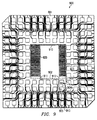
- FIG. 9 is the top view of the substrate generally designated 900 of a ball grid array package for a semiconductor device requiring 144 ball connections (on the bottom surface of the substrate, not shown in FIG. 9).
- the insulating layer 901 of the substrate is made of organic material in the thickness range from about 70 to 150 ⁇ m, as mentioned in conjunction with FIG. 1.
- the dotted line 902 encloses the area reserved for attaching the IC chip. Substantially within this area are accommodated one inductance 910 and one capacitor 920 of the low pass filter of the invention.
- the one lead 911 of the inductance 910 originates with the metallization 903, cooperatively intended for a bonding wire stitch terminal.
- the other lead 912 of the inductance 903 is placed on terminal pad 904a, which connects to a metal-filled via and a solder ball (not shown in FIG. 9).
- metal line 913 is connected to the applied plating potential.
- the inductance lead 912 further doubles as the "inner” comb terminal of capacitor 920.
- the "outer” comb 922 is connected to terminal pad 904b, which connects to a metal-filled via and a solder ball at ground potential (not shown in FIG. 9).
- metal line 923 is connected to the allied plating potential.
- the material of the semiconductor chip may comprise silicon, silicon germanium, gallium arsenide, or any other semiconductor material used in manufacturing.
- the package may be a BGA package or any other semiconductor device package.
- the electrical characteristics of inductance and/or capacitance of the low pass filter can be modified in order to attenuate or filter different regimes of the frequency spectrum.
- the geometrical layout of capacitance and/or inductance of the low pass filter can be patterned differently, if the IC chip is attached to the substrate by a flip-solder process instead by adhesive and wire bonding. It is therefore intended that the appended claims encompass any such modifications or embodiments.
Landscapes
- Semiconductor Integrated Circuits (AREA)
- Structures For Mounting Electric Components On Printed Circuit Boards (AREA)
Abstract
Description
Claims (15)
- A semiconductor package substrate (803) for assembling an integrated circuit chip (801) operable at fast ramp rate signals and clock rates, comprising:an insulating support (802) having a region for attaching said chip (801);a pattern of electrical interconnections (807, 808, 809), disposed on said substrate in one metallization level and operable for transmitting waveforms; anda low pass filter (820) for removing unwanted high frequency components from said transmitted waveforms, comprising a network of inductors and capacitors formed within said one metallization level and positioned substantially within said substrate region for chip attachment.
- The substrate according to Claim 1 wherein said semiconductor package is a ball grid array package.
- The substrate according to Claim 1 wherein said network comprises at least one inductor and one capacitor.
- The substrate according to Claim 1 wherein said network further comprises at least one resistor.
- The substrate according to Claim 1 wherein said unwanted high frequency components are in the frequency range up to about 10 GHz.
- A semiconductor package substrate (803) for assembling a high frequency integrated circuit chip (801), comprising:an insulating support (802) having a region for attaching said chip (801);a pattern of electrical interconnections (807, 808, 809) disposed on said substrate in one metallization level, at least one them having the unwanted property of emitting high frequency radiation; anda low pass filter (820) for attenuating said radiation, comprising a network of inductors and capacitors formed within said one metallization level and positioned substantially within said substrate region for chip attachment, whereby said substrate preserves fast ramp rate signals and clock rates of said integrated circuit.
- The substrate according to Claim 6 wherein said semiconductor package is a ball grid array package.
- The substrate according to Claim 6 whereby said network includes narrow and wide traces suitable for filtering radio frequency radiation.
- The substrate according to Claim 6 wherein said filter can be changed as needed to address differences in characteristics of said circuit or the assembly board.
- The substrate according to Claim 6 wherein said unwanted radiation is in the frequency range up to about 10 GHz.
- A method for fabricating a semiconductor package substrate (803) having a region for attaching a high frequency integrated circuit chip, comprising the steps of:providing a substrate (803) having an insulating layer with first and second surfaces;forming a plurality of openings in said insulating layer;depositing a metal film onto said insulating layer over said first surface; andpatterning said metal film to create a network of capacitors and inductors forming a low pass filter (820) for high frequency radiation, said network located within said region for attaching said chip, and concurrently to create electrical contact terminals (807, 809, 810) above and within said openings.
- The method according to Claim 11 further comprising the steps of:depositing a film of solderable metal over said second surface of said insulating layer; andpatterning said metal film to create electrical contact terminals suitable for attaching solder balls.
- The method according to Claim 11 wherein said semiconductor package is a ball grid array package.
- The method according to Claim 11 further comprising the step of depositing additional metal on top of said metal film after said patterning.
- The method according to Claim 14 wherein said additional metal is deposited by an electroplating process.
Applications Claiming Priority (2)
| Application Number | Priority Date | Filing Date | Title |
|---|---|---|---|
| US15431399P | 1999-09-16 | 1999-09-16 | |
| US154313P | 1999-09-16 |
Publications (2)
| Publication Number | Publication Date |
|---|---|
| EP1085572A2 true EP1085572A2 (en) | 2001-03-21 |
| EP1085572A3 EP1085572A3 (en) | 2006-04-19 |
Family
ID=22550849
Family Applications (1)
| Application Number | Title | Priority Date | Filing Date |
|---|---|---|---|
| EP20000118141 Withdrawn EP1085572A3 (en) | 1999-09-16 | 2000-08-29 | Low pass filter integral with semiconductor package |
Country Status (4)
| Country | Link |
|---|---|
| US (1) | US6424027B1 (en) |
| EP (1) | EP1085572A3 (en) |
| JP (1) | JP2001094014A (en) |
| KR (1) | KR100801374B1 (en) |
Cited By (2)
| Publication number | Priority date | Publication date | Assignee | Title |
|---|---|---|---|---|
| WO2003026006A3 (en) * | 2001-08-30 | 2003-08-07 | Infineon Technologies Ag | Arrangement of a semiconductor in a housing, chip card and chip module |
| EP1411553A4 (en) * | 2001-07-12 | 2008-09-03 | Hitachi Ltd | ELECTRONIC CIRCUIT COMPONENT |
Families Citing this family (19)
| Publication number | Priority date | Publication date | Assignee | Title |
|---|---|---|---|---|
| DE60040741D1 (en) | 1999-04-20 | 2008-12-18 | Illumina Inc | DETECTION OF NUCLEINE ACID REACTIONS ON BEADLE ARRAYS |
| US6577018B1 (en) * | 2000-08-25 | 2003-06-10 | Micron Technology, Inc. | Integrated circuit device having reduced bow and method for making same |
| KR100411811B1 (en) * | 2001-04-02 | 2003-12-24 | 앰코 테크놀로지 코리아 주식회사 | Semiconductor package |
| US6759921B1 (en) * | 2001-08-17 | 2004-07-06 | Lsi Logic Corporation | Characteristic impedance equalizer and an integrated circuit package employing the same |
| SG102637A1 (en) * | 2001-09-10 | 2004-03-26 | Micron Technology Inc | Bow control in an electronic package |
| US7138884B2 (en) * | 2002-08-19 | 2006-11-21 | Dsp Group Inc. | Circuit package integrating passive radio frequency structure |
| US8222721B2 (en) * | 2003-09-15 | 2012-07-17 | Silicon Laboratories Inc. | Integrated circuit suitable for use in radio receivers |
| US7064419B1 (en) | 2004-06-18 | 2006-06-20 | National Semiconductor Corporation | Die attach region for use in a micro-array integrated circuit package |
| US7259460B1 (en) | 2004-06-18 | 2007-08-21 | National Semiconductor Corporation | Wire bonding on thinned portions of a lead-frame configured for use in a micro-array integrated circuit package |
| US7087986B1 (en) * | 2004-06-18 | 2006-08-08 | National Semiconductor Corporation | Solder pad configuration for use in a micro-array integrated circuit package |
| US7545031B2 (en) * | 2005-04-11 | 2009-06-09 | Stats Chippac Ltd. | Multipackage module having stacked packages with asymmetrically arranged die and molding |
| KR100723491B1 (en) * | 2005-07-14 | 2007-05-30 | 삼성전자주식회사 | Universal Printed Circuit Boards and Smart Cards Using the Same |
| JP2007128339A (en) * | 2005-11-04 | 2007-05-24 | Matsushita Electric Ind Co Ltd | Semiconductor device package design method, layout design tool for implementing the method, and semiconductor prosecution manufacturing method using the same |
| US7608482B1 (en) | 2006-12-21 | 2009-10-27 | National Semiconductor Corporation | Integrated circuit package with molded insulation |
| KR100951695B1 (en) | 2007-12-24 | 2010-04-07 | (주)페타리 | Isolator and its manufacturing method |
| JP2009194196A (en) * | 2008-02-15 | 2009-08-27 | Nec Electronics Corp | Semiconductor device manufacturing method and semiconductor device |
| JP4860661B2 (en) * | 2008-05-23 | 2012-01-25 | 富士通セミコンダクター株式会社 | Semiconductor package design method and semiconductor package layout design apparatus |
| CN115235620B (en) * | 2022-07-20 | 2025-03-18 | 北京量子信息科学研究院 | Single photon detection device and single photon detection method |
| CN116190336B (en) * | 2023-02-15 | 2026-02-03 | 湖北九峰山实验室 | Radio frequency integrated equipment and preparation method thereof |
Family Cites Families (7)
| Publication number | Priority date | Publication date | Assignee | Title |
|---|---|---|---|---|
| JPS594175A (en) * | 1982-06-30 | 1984-01-10 | Fujitsu Ltd | Field effect semiconductor device |
| JPS61208919A (en) * | 1985-03-13 | 1986-09-17 | Toshiba Corp | Low pass filter built in integrated circuit |
| JPH06268532A (en) * | 1993-03-12 | 1994-09-22 | Tdk Corp | MMIC package |
| JPH07273502A (en) * | 1994-03-29 | 1995-10-20 | Murata Mfg Co Ltd | Low pass filter |
| US5428245A (en) * | 1994-05-06 | 1995-06-27 | National Semiconductor Corporation | Lead frame including an inductor or other such magnetic component |
| JPH1084074A (en) * | 1996-09-09 | 1998-03-31 | Mitsubishi Electric Corp | Semiconductor package |
| JP3147053B2 (en) * | 1997-10-27 | 2001-03-19 | 日本電気株式会社 | Resin-sealed ball grid array IC package and method of manufacturing the same |
-
2000
- 2000-08-29 EP EP20000118141 patent/EP1085572A3/en not_active Withdrawn
- 2000-09-12 US US09/659,927 patent/US6424027B1/en not_active Expired - Lifetime
- 2000-09-14 JP JP2000280236A patent/JP2001094014A/en not_active Abandoned
- 2000-09-15 KR KR20000054123A patent/KR100801374B1/en not_active Expired - Fee Related
Cited By (3)
| Publication number | Priority date | Publication date | Assignee | Title |
|---|---|---|---|---|
| EP1411553A4 (en) * | 2001-07-12 | 2008-09-03 | Hitachi Ltd | ELECTRONIC CIRCUIT COMPONENT |
| US7586755B2 (en) | 2001-07-12 | 2009-09-08 | Hitachi, Ltd. | Electronic circuit component |
| WO2003026006A3 (en) * | 2001-08-30 | 2003-08-07 | Infineon Technologies Ag | Arrangement of a semiconductor in a housing, chip card and chip module |
Also Published As
| Publication number | Publication date |
|---|---|
| US6424027B1 (en) | 2002-07-23 |
| KR20010067180A (en) | 2001-07-12 |
| JP2001094014A (en) | 2001-04-06 |
| EP1085572A3 (en) | 2006-04-19 |
| KR100801374B1 (en) | 2008-02-05 |
Similar Documents
| Publication | Publication Date | Title |
|---|---|---|
| US6424027B1 (en) | Low pass filter integral with semiconductor package | |
| KR100612425B1 (en) | Structure and Manufacturing Method of Lead-free Chip Carrier with Antenna | |
| US7795072B2 (en) | Structure and method of high performance two layer ball grid array substrate | |
| US8598690B2 (en) | Semiconductor device having conductive vias in peripheral region connecting shielding layer to ground | |
| US5858815A (en) | Semiconductor package and method for fabricating the same | |
| US6707168B1 (en) | Shielded semiconductor package with single-sided substrate and method for making the same | |
| US5784261A (en) | Microchip module assemblies | |
| US20020070451A1 (en) | Semiconductor device having a ball grid array and method therefor | |
| US20130118008A1 (en) | Thermal interface material application for integrated circuit cooling | |
| KR20040030966A (en) | Structure and method for fabrication of a leadless chip carrier with embedded inductor | |
| WO2002089207A2 (en) | High performance, low cost microelectronic circuit package with interposer | |
| US5977624A (en) | Semiconductor package and assembly for fabricating the same | |
| US6395995B1 (en) | Apparatus for coupling integrated circuit packages to bonding pads having vias | |
| KR102422055B1 (en) | Printed circuit board | |
| US12506252B2 (en) | Fan-out package structure and fabrication method therefor | |
| JP3413147B2 (en) | Multi-line grid array package | |
| US9673137B2 (en) | Electronic device having a lead with selectively modified electrical properties | |
| US20030116776A1 (en) | Substrate stack | |
| RU2860363C1 (en) | Monolithic integrated circuit | |
| EP1079433A2 (en) | Ball grid array package having two ground levels | |
| TW202527315A (en) | Electronic component | |
| CN117174691A (en) | Radio frequency module chip and preparation method thereof | |
| JP2001185654A (en) | Electronic package with integrated filter | |
| Tsukada | A Key Role of Printed Circuit Board in Recent Packaging Technology | |
| Murakami | Semiconductor packaging technology for mobile phones in Japan |
Legal Events
| Date | Code | Title | Description |
|---|---|---|---|
| PUAI | Public reference made under article 153(3) epc to a published international application that has entered the european phase |
Free format text: ORIGINAL CODE: 0009012 |
|
| AK | Designated contracting states |
Kind code of ref document: A2 Designated state(s): AT BE CH CY DE DK ES FI FR GB GR IE IT LI LU MC NL PT SE |
|
| AX | Request for extension of the european patent |
Free format text: AL;LT;LV;MK;RO;SI |
|
| PUAL | Search report despatched |
Free format text: ORIGINAL CODE: 0009013 |
|
| AK | Designated contracting states |
Kind code of ref document: A3 Designated state(s): AT BE CH CY DE DK ES FI FR GB GR IE IT LI LU MC NL PT SE |
|
| AX | Request for extension of the european patent |
Extension state: AL LT LV MK RO SI |
|
| 17P | Request for examination filed |
Effective date: 20061006 |
|
| AKX | Designation fees paid |
Designated state(s): DE FR GB |
|
| 17Q | First examination report despatched |
Effective date: 20090217 |
|
| STAA | Information on the status of an ep patent application or granted ep patent |
Free format text: STATUS: THE APPLICATION IS DEEMED TO BE WITHDRAWN |
|
| 18D | Application deemed to be withdrawn |
Effective date: 20091028 |