EP1085524A1 - Structure and method with which to generate data background patterns for testing random-access-memories - Google Patents
Structure and method with which to generate data background patterns for testing random-access-memories Download PDFInfo
- Publication number
- EP1085524A1 EP1085524A1 EP00305838A EP00305838A EP1085524A1 EP 1085524 A1 EP1085524 A1 EP 1085524A1 EP 00305838 A EP00305838 A EP 00305838A EP 00305838 A EP00305838 A EP 00305838A EP 1085524 A1 EP1085524 A1 EP 1085524A1
- Authority
- EP
- European Patent Office
- Prior art keywords
- data
- ram
- data bit
- programming information
- background pattern
- Prior art date
- Legal status (The legal status is an assumption and is not a legal conclusion. Google has not performed a legal analysis and makes no representation as to the accuracy of the status listed.)
- Withdrawn
Links
Images

Classifications
-
- G—PHYSICS
- G11—INFORMATION STORAGE
- G11C—STATIC STORES
- G11C29/00—Checking stores for correct operation ; Subsequent repair; Testing stores during standby or offline operation
- G11C29/04—Detection or location of defective memory elements, e.g. cell constructio details, timing of test signals
- G11C29/08—Functional testing, e.g. testing during refresh, power-on self testing [POST] or distributed testing
- G11C29/12—Built-in arrangements for testing, e.g. built-in self testing [BIST] or interconnection details
- G11C29/36—Data generation devices, e.g. data inverters
-
- G—PHYSICS
- G11—INFORMATION STORAGE
- G11C—STATIC STORES
- G11C29/00—Checking stores for correct operation ; Subsequent repair; Testing stores during standby or offline operation
- G11C29/04—Detection or location of defective memory elements, e.g. cell constructio details, timing of test signals
- G11C29/08—Functional testing, e.g. testing during refresh, power-on self testing [POST] or distributed testing
- G11C29/12—Built-in arrangements for testing, e.g. built-in self testing [BIST] or interconnection details
- G11C29/18—Address generation devices; Devices for accessing memories, e.g. details of addressing circuits
- G11C29/30—Accessing single arrays
- G11C29/32—Serial access; Scan testing
Definitions
- This invention relates generally to integrated circuits memory devices, and more particularly to an improved apparatus and method for generating data background patterns used for testing random access memories.
- Random access memories are typically tested using an external test machine, such as a state machine, or a built-in-self-test (BIST) machine that provides predefined patterns able to identify faulty memory cells of the memory array. Testing aids in the discovery of certain faulty cells and is key to the proper characterization of the RAM.
- the predefined patterns are defined by engineers and can be considered sufficiently discriminatory to provide an adequate information concerning the state of one or more memory cells, whether it be a good, repairable, or fail state, for instance.
- a predefined testing pattern may be thought of as having two parts. The first part includes the commands, such as read, write, wait, etc., for testing the memory cells and the addresses of the memory cells to be tested.
- the second part of a predefined pattern is the pattern itself comprised of the data pattern and the background pattern.
- march patterns are commonly used to test RAM memories.
- march patterns available for testing memories; a few march patterns commonly used to test memories include MATS, MATS+, MATS++, MARCHX, MARCHC-, MARCHA, MARCHY, MARCHB, MARCHLR, MARINESCU.
- Not all march testing patterns detect all faults of a RAM and thus different types of march testing patterns are used to detect different RAM faults.
- Some types of march patterns are designed to target specific types of faults while others seek to identify as many faults as possible.
- march testing patterns include stuck at faults (SAFs), transition faults (TFs), coupling faults (CFs), address decoder faults (AFs), state coupling faults (SCFs), and bridging faults (BFs).
- SAFs stuck at faults
- TFs transition faults
- CFs coupling faults
- AFs address decoder faults
- SCFs state coupling faults
- BFs bridging faults
- intraword faults a special set of faults, called intraword faults, that exist between two or more bits of a word in a memory array.
- intraword faults are identified by applying traditional march patterns to a word-oriented memory and repeating the test the required number of times using multiple data backgrounds, where the data background refers to the data applied to a complete word.
- the internal BIST machine solution while it does not have this pin-out limitation, is a problematic solution in its own right.
- the BIST machine that provides patterns and backgrounds becomes more and more complex, each individual data needing a driver and more complex algorithms to properly test the memory.
- the number of gates of the BIST machine can be expected to increase at least at the same rate of increase of the data bus width, if not more, as the number of requested data backgrounds required to completely test the memory array may increase more rapidly.
- a large number of signals which occupy a large area of the routing channel of the memory is called for.
- the BIST machine solution is a solid-state solution embedded in the silicon of the memory array device and is therefore inherently inflexible with regard to the type of patterns that it employs to test the memory array.
- the BIST machine is hard to modify should a pattern be missing Using the BIST solution, it is impossible to later add a "forgotten" pattern without fabricating a new maskset for the BIST circuitry since the BIST solution is embedded in silicon.
- FIG. 1 a block diagram illustrates a possible scenario for testing an embedded memory array that is controlled by a controller of the device on which the memory is embedded.
- the data patterns for testing the memory are provided by a test machine which may be either a BIST machine or an external test machine, as discussed above.
- the testing data provided by the test machine is multiplexed with information from the controller as shown.
- Information from the memory array is likewise multiplexed before being provided to the controller that in turn provides the results of the memory testing to the test machine.
- the greatly increased number of gates required in the test machine, particularly if the test machine is a BIST machine, as well as the number of multiplexers required to adequately test RAMs having ever-increasing data bus widths can serious degrade device performance.
- These increased demands in silicon are evidenced by the great number of wires, or routing, that is illustrated between the test machine and the multiplexer circuitry, between the multiplexer circuitry and the memory array, and between the multiplexer circuitry and the controller.
- the improved method and structure should accommodate testing of RAMs having ever-increasing data bus widths by both BIST machines and external test machines.
- the number of additional package pins and additional silicon of the RAM should be kept to a minimum while providing for maximum testing flexibility.
- an improved apparatus and method for generating data background patterns for testing random-access-memories includes circuitry of a RAM that comprises a programming element and a selection element.
- the programming element is able to selectively program desired bits of a data background pattern according to a programming information signal provided to the RAM in order to generate a programmed data background pattern.
- the selection element receives the programmed data background pattern as well as a normal, application data and selects and outputs to an input/output buffer of the RAM either the programmed data background pattern or application data according to the logic state of a test control signal.
- the programming element for each data bit of the data background pattern the programming element comprises a shift register element that receives a programming information signal and a clock signal and shifts in and outputs the programming information signal in accordance with the clock signal and a logic element that receives the programming information signal from the shift register and a data bit of a data background pattern and performs an exclusive-or (XOR) function on the programming information signal and the data bit of the data background pattern to generate a programmed data bit.
- XOR exclusive-or
- the selection element For each data bit of the data background pattern the selection element comprises a multiplexer element controlled by a test control signal that receives an application data bit and the programmed data bit, wherein when the test control signal is a first logic state indicative of a testing mode of the RAM the multiplexer element selects and outputs the programmed data bit to an input/output buffer of the RAM and when the test control signal is a second logic state indicative of a normal operating mode of the RAM the multiplexer element selects and outputs the application data bit to the input/output buffer of the RAM.
- the methodology of the present invention accomplishes the goal of programmability of data background patterns used to test a RAM by providing a data background pattern to the RAM, providing a programming information signal to the RAM, selectively programming the data bits of the data background pattern in accordance with the programming information signal to generate a programmed test data pattern, and providing the programmed test data pattern to an input/output buffer of the RAM when the RAM is in a testing mode as indicated by a test control signal.
- the methodology is further capable of providing an application data to the input/output data when the RAM is in a normal operating mode as indicated by the test control signal.
- the programming information signal is provided to the RAM by using a shift register to shift in this information and programmability of the various bits of the data background pattern are programmed using an exclusive-OR (XOR) gating function that receives the programming information signal and an appropriate bit of the data background pattern.
- XOR exclusive-OR
- one skilled in the art may accomplish the methodology of the present invention using a different structure on the RAM so long as the functionality of the methodology is accomplished.
- the improved circuitry structure of the present invention consists of adding to the memory input/output (I/O) buffers of an embedded RAM memory one or more shift registers that may be used as programming mechanism for data background patterns, akin to a "mask," although not in silicon, to selectively invert or not invert the data background patterns and thereby provide programmability of the types and compositions of data background patterns used to test the memory.
- the I/O buffers are able to provide any data background for testing of a random access memory device.
- the present invention especially lends itself to the testing of word-oriented RAM memories characterized as having more than 1-bit per word.
- a shift register and gating circuitry is added to the I/O buffer of the embedded memory array for each data bit of the address data bit for which programmability is desired.
- circuitry 10 of Figure 2 by way of illustration three placements 20, 40, and 60 of the present invention, one for each of three data bits present on the DATA_IN_TEST bus 15 in this particular example. It will be recognized in the art that the number of placements of the invention is a function of the number of data bits present on the DATA_IN_TEST bus 15.
- Each placement of the invention includes a shift register that receives and shifts in programming information according to a clock signal, an exclusive-OR (XOR) gate or its equivalent that receives the output signal from the preceding shift register and gates it with the DATA_IN_TEST data bit provided to it, and a multiplexer.
- the multiplexer selects and outputs the output of the XOR gate in the test mode when the TEST control signal is a high logic state and selects and outputs application data provided to it when the TEST control signal is a low logic state.
- the programming information signal 26 of the first shift register 22 is provided externally to circuitry 10 by an on-chip BIST machine or an external tester, while the programming information signal of subsequent shift registers is provided by the output signal of the preceding shift register.
- the programming information signal of shift register 42 is the output signal 28 of the preceding shift register 22 and similarly the programming information signal of shift register 62 is the output signal 44 of its preceding shift register 42.
- shift register 22 shifts in programming information signal 26 in accordance with clock signal 24 and outputs signal 28.
- Signal 28 is the input programming information signal to subsequent shift register 42 in placement 40 as well as being an input to XOR gate 30.
- the output signal 31, then, of XOR gate 30 reflects the appropriate, i.e. inverted or non-inverted, state of data bit 15i.
- data bit DINi 32 is multiplexed with a single input DATA_IN_TEST bit 31 representative of regular application data to be provided to the I/O buffers of the RAM when in a non-testing, normal operation mode.
- the TEST control signal 34 indicates whether the RAM is in a testing mode or a normal operating mode and thus which in put data to the multiplexer, the regular data Din or the test data output from the XOR gate, will be selected and passed through to the I/O buffers (read or write) of the RAM.
- TEST control signal 34 is a high (“1") logic state
- the RAM test mode is indicated and thus the output signal 31 of XOR gate 30 is selected and passed through the multiplexer 36 as signal 38.
- TEST control signal 34 is a low (“0") logic state
- the RAM is in the normal operating mode and thus the normal application data DINi 32 is selected by multiplexer 36 and passed through as signal 38.
- the second placement 40 of the present invention operates in a similar manner.
- Shift register 42 shifts in programming information signal 28, generated by shift register 22, in accordance with clock signal 24 and outputs signal 44.
- Signal 44 is the input programming information signal of subsequent shift register 62 in placement 60 as well as being an input to XOR gate 66.
- the output signal 48, then, of XOR gate 46 reflects the appropriate, i.e.
- data bit DINj 50 is multiplexed with a single input DATA_IN_TEST bit 48 representative of regular application data to be provided to the I/O buffers of the RAM when in a non-testing, normal operation mode.
- the TEST control signal 34 indicates whether the RAM is in a testing mode or a normal operating mode and thus which input data to the multiplexer, the regular data Din or the test data output from the XOR gate, will be selected and passed through to the I/O buffers (read or write) of the RAM.
- TEST control signal 34 When TEST control signal 34 is a high ("1") logic state, the RAM test mode is indicated and thus the output signal 48 of XOR gate 46 is selected and passed through the multiplexer 54 as signal 56.
- TEST control signal 34 When, on the other hand, TEST control signal 34 is a low (“0") logic state, the RAM is in the normal operating mode and thus the normal application data DINj 50 is selected by multiplexer 54 and passed through as signal 56.
- shift register 62 shifts in programming information signal 44 in accordance with clock signal 24 and outputs signal 64.
- Signal 64 is the input programming information signal to a shift register is any subsequent placements of the invention (not shown) as well as being an input to XOR gate 66.
- the output signal 68, then, of XOR gate 66 reflects the appropriate, i.e.
- data bit DINk 70 is multiplexed with a single input DATA_IN_TEST bit 68 representative of regular application data to be provided to the I/O buffers of the RAM when in a non-testing, normal operation mode.
- the TEST control signal 34 indicates whether the RAM is in a testing mode or a normal operating mode and thus which input data to the multiplexer, the regular data Din or the test data output from the XOR gate, will be selected and passed through to the I/O buffers (read or write) of the RAM.
- TEST control signal 34 When TEST control signal 34 is a high ("1") logic state, the RAM test mode is indicated and thus the output signal 68 of XOR gate 66 is selected and passed through the multiplexer 72 as signal 74.
- TEST control signal 34 When, on the other hand, TEST control signal 34 is a low (“0") logic state, the RAM is in the normal operating mode and thus the normal application data DINk 70 is selected by multiplexer 72 and passed through as signal 74.
- DATA_IN_TEST data pattern bus 15 will be in the same testing mode at a given time, i.e. simultaneously subject to the same testing command such as "Read” or “Write” or “Idle” at the same time, etc., and must therefore be treated in parallel, the only difference between two parallel data is its background which is representative of its logical value during a testing access of the RAM.
- the shift register circuitry of Figure 1 thus uses only one or a limited number of DATA_IN_TEST inputs per placement of the invention thereby simplifying the routing channels of the RAM since only one or a small number of extra connections is required to provide testing information to the RAM.
- certain "mask” or programming information signal 26 is shifted into the shift register.
- This programming information 26 will either cause data background pattern bus DATA_IN_TEST data bits 15i, 15j, 15k to be inverted (if one) or not inverted (if zero), thereby allowing any possible data background for a given pattern to be easily applied into the RAM, at almost no silicon expense.
- the number of testing patterns is virtually unlimited because all 2 n combination on an n-bit bus can be applied, one after the other.
- the external tester of the memory device is greatly simplified or, if using a BIST machine, test development complexity is greatly reduced by providing only one data information rather than having to increase the data bus width of the array in order to accomplish testing.
- the routage between the BIST or external testing machine and the RAM memory(ies) is limited to three wires for DATA_IN_TEST bus 15, programming information signal 26, and clock signal 24, exclusive of the diagnostic signals coming from the memory. This routage will be remain the same for all memory formats, with the length of the shift register (number of placements) being the main parameter to control. Control can be provided directly by a BIST machine or the external test equipment to ensure programmability.
- the test pattern content of the shift register is provided by any appropriate state machine, which may be either external or internal to the RAM.
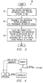
- the methodology of the present invention is shown by flowchart 80 of Figure 3 . It is hereby noted that this methodology may be implemented using the circuitry of Figure 1 or other structures capable of providing the same methodology.
- the first step of the methodology is that the RAM receives programming information provided to it from an external source, such as by the BIST machine or external testing equipment.
- the structural embodiment of Figure 1 implements this step by the shift register receiving programming information signal 26.
- a data background pattern is programmed according to the programming information that has been received at Block 82. In Figure 1, this is accomplished by the XOR gating function that programs the data bit from DATA_IN_TEST data bus 15 according to the output signal 28 of shift register 22.
- a decision about which type of data to provide to I/O buffers of the RAM, either test data or application data, is made according to a test mode control signal.
- the programmed data background pattern is selected and provided to the I/O buffers of the RAM if the test control signal indicates that the RAM is in a testing mode during which the programmed data pattern data would be needed by the RAM.
- the application data is selected and provided to the I/O buffers of the RAM if the test control signal indicates that the RAM is in a normal operating mode during which regular application data is needed by the RAM.
- FIG. 4 an example of the present invention in an embedded memory environment is illustrated.
- the advantages of this block diagram over the prior art block diagram of Figure 1 are clear.
- the circuitry of Figure 2 is incorporated in the Memory block. It can be seen that the only one extra input pin of the Memory is necessary to provide the data patterns (DATA_IN_TEST) for testing the Memory from the Test Machine, whether an internal BIST machine that resides with the embedded memory on the device or an external test machine outside the device, to the circuitry of Figure 2 which resides inside the Memory block. Diagnostic information, such as pass, fail, idle, etc., is provided to the Test Machine directly from the Memory as shown.
- DATA_IN_TEST data patterns
- the Test Machine is reduced to a single output pattern generator that provides data patterns for testing and thus occupies very little silicon of the device, if an internal BIST machine. Moreover, the Test Machine correspondingly consumes much less energy since there is only one I/O buffer to which data is supplied, instead of the 128 or 256 buffers that might be required in the prior art Figure 2, for example, in the case of a 128 bit or 256 bit wide data bus.
- the present invention allows a drastic simplification of the test machine by reducing the number of gates required while at the same time providing complete programmability of the backgrounds for a given testing pattern.
- the complexity of the test machine is greatly reduced as only one data signal need be provided to the shift register circuitry; thus only one extra pin is required on the memory device to provide the data patterns from the test machine.
- the simplification in number of gates is estimated to be between a factor of 10 to 100, without even taking into account the enhancement in programmability of the invention.
- the present invention eliminates the need to drive all 8 bits at the same time in order to adequately test the memory.
- the BIST or external tester can load the pattern through the shift register and apply it to the exclusive OR (XORs) gates.
- XORs exclusive OR
- the external or BIST tester therefore need only provide a '1' or '0' as stimulus since the testing patterns are generated by the XORs functionality.
Landscapes
- Tests Of Electronic Circuits (AREA)
- Techniques For Improving Reliability Of Storages (AREA)
- For Increasing The Reliability Of Semiconductor Memories (AREA)
Abstract
Programmability of the data background patterns used to test random-access-memories
(RAMs) is accomplished by adding to the memory input/output
(I/O) buffers of RAM memory, for each data bit of a data background pattern to be
programmed, a programming mechanism and a selection mechanism. The
programming mechanism is capable of programming a data bit of the data
background pattern in accordance with a programming information signal provided
to the RAM. The selection mechanism provides either the programmed data bit or a
normal, application data bit to an input/output buffer of the RAM in accordance with
whether the RAM is in a test mode or a normal operating mode, as indicated by a
test control signal provided to the RAM.
Description
This invention relates generally to integrated circuits memory devices, and
more particularly to an improved apparatus and method for generating data
background patterns used for testing random access memories.
Random access memories (RAMs) are typically tested using an external test
machine, such as a state machine, or a built-in-self-test (BIST) machine that
provides predefined patterns able to identify faulty memory cells of the memory
array. Testing aids in the discovery of certain faulty cells and is key to the proper
characterization of the RAM. For both the external test machine and the BIST
machine cases the predefined patterns are defined by engineers and can be
considered sufficiently discriminatory to provide an adequate information concerning
the state of one or more memory cells, whether it be a good, repairable, or fail state,
for instance. A predefined testing pattern may be thought of as having two parts.
The first part includes the commands, such as read, write, wait, etc., for testing the
memory cells and the addresses of the memory cells to be tested. The second part
of a predefined pattern is the pattern itself comprised of the data pattern and the
background pattern.
So-called "march" patterns are commonly used to test RAM memories. There
are many different march patterns available for testing memories; a few march
patterns commonly used to test memories include MATS, MATS+, MATS++,
MARCHX, MARCHC-, MARCHA, MARCHY, MARCHB, MARCHLR, MARINESCU.
Not all march testing patterns detect all faults of a RAM and thus different types of
march testing patterns are used to detect different RAM faults. Some types of
march patterns are designed to target specific types of faults while others seek to
identify as many faults as possible. The various types of faults that can be identified
by march testing patterns include stuck at faults (SAFs), transition faults (TFs),
coupling faults (CFs), address decoder faults (AFs), state coupling faults (SCFs),
and bridging faults (BFs). The common characteristic of all march patterns,
however, is that a sequence of events, such as reads and writes, for instance, are
applied to one address of the memory array before moving onto the next address of
the memory array being tested. This testing sequence is repeated in an ascending
or descending order, as dictated by the particular march algorithm, throughout the
address space being tested.
The testing of word-oriented memories which have more than 1-bit per word
present a special testing problem. In a word-oriented memory, allowances have to
be made to the traditional march patterns in order to accommodate the detection of
a special set of faults, called intraword faults, that exist between two or more bits of
a word in a memory array. Typically intraword faults are identified by applying
traditional march patterns to a word-oriented memory and repeating the test the
required number of times using multiple data backgrounds, where the data
background refers to the data applied to a complete word. As an example, consider
the following simple sequence of a march pattern:
/{w0r0w1r1}
which means to "write zero, read zero, write 1, read 1" starting at the lowest memory address and progressing to the highest memory address of the memory array to be tested. This sequence is very straightforward for a single-bit-wide memory, but is more complex for a word-oriented memory in which the '0' means "data background" and the '1' means "inverted data background." So, '0' might be represented by any of the following data background patterns: 00000000, 01010101, 00110011, 00001111; '1' would be represented by the inverse of these data background patterns. To apply these background patterns, the marching pattern algorithm would be repeated using each of these background patterns in place of the '1' or '0' in the above sequence. Thus for an 8-bit wide memory there are 256 possible data backgrounds implicated by this sequence. Typically, however, only log2N+1 data backgrounds, where N refers to the number of bits per word, are used in order to help reduce testing time.
/{w0r0w1r1}
which means to "write zero, read zero, write 1, read 1" starting at the lowest memory address and progressing to the highest memory address of the memory array to be tested. This sequence is very straightforward for a single-bit-wide memory, but is more complex for a word-oriented memory in which the '0' means "data background" and the '1' means "inverted data background." So, '0' might be represented by any of the following data background patterns: 00000000, 01010101, 00110011, 00001111; '1' would be represented by the inverse of these data background patterns. To apply these background patterns, the marching pattern algorithm would be repeated using each of these background patterns in place of the '1' or '0' in the above sequence. Thus for an 8-bit wide memory there are 256 possible data backgrounds implicated by this sequence. Typically, however, only log2N+1 data backgrounds, where N refers to the number of bits per word, are used in order to help reduce testing time.
Compounding the complexity of testing word-oriented memories is the ever-increasing
width of the data bus of the memory array. Current data bus widths of
memory devices are 64 bits and data bus widths upwards of 256/512 bits are
expected in the near future. The increased width of the data bus is exponential in
nature, doubling about every 9 to 10 months or so. In the case of an external test
machine, such increased data bus widths cannot be easily handled by an external
tester because the number of package pins is strictly limited by the application. For
instance, a package housing a memory array device might have only 100 to 200
pins, a number of pins insufficient to handle testing a data bus having a width of 256
or 512 bits.
The internal BIST machine solution, while it does not have this pin-out
limitation, is a problematic solution in its own right. With the always increasing width
of the data bus, the BIST machine that provides patterns and backgrounds becomes
more and more complex, each individual data needing a driver and more complex
algorithms to properly test the memory. The number of gates of the BIST machine
can be expected to increase at least at the same rate of increase of the data bus
width, if not more, as the number of requested data backgrounds required to
completely test the memory array may increase more rapidly. In order for the BIST
solution to support greatly expanded data bus widths, a large number of signals
which occupy a large area of the routing channel of the memory is called for.
Moreover, the BIST machine solution is a solid-state solution embedded in the
silicon of the memory array device and is therefore inherently inflexible with regard
to the type of patterns that it employs to test the memory array. The BIST machine
is hard to modify should a pattern be missing Using the BIST solution, it is
impossible to later add a "forgotten" pattern without fabricating a new maskset for
the BIST circuitry since the BIST solution is embedded in silicon.
Referring to Figure 1, a block diagram illustrates a possible scenario for
testing an embedded memory array that is controlled by a controller of the device on
which the memory is embedded. The data patterns for testing the memory are
provided by a test machine which may be either a BIST machine or an external test
machine, as discussed above. The testing data provided by the test machine is
multiplexed with information from the controller as shown. Information from the
memory array is likewise multiplexed before being provided to the controller that in
turn provides the results of the memory testing to the test machine. The greatly
increased number of gates required in the test machine, particularly if the test
machine is a BIST machine, as well as the number of multiplexers required to
adequately test RAMs having ever-increasing data bus widths can serious degrade
device performance. These increased demands in silicon are evidenced by the
great number of wires, or routing, that is illustrated between the test machine and
the multiplexer circuitry, between the multiplexer circuitry and the memory array, and
between the multiplexer circuitry and the controller.
From the foregoing description, it can be seen that there is a need in the art
to have an improved method and structure for the testing of RAMs. The improved
method and structure should accommodate testing of RAMs having ever-increasing
data bus widths by both BIST machines and external test machines. The number of
additional package pins and additional silicon of the RAM should be kept to a
minimum while providing for maximum testing flexibility.
According to the principles of the present invention, an improved apparatus
and method for generating data background patterns for testing random-access-memories
is provided. The improved apparatus of the present invention includes
circuitry of a RAM that comprises a programming element and a selection element.
The programming element is able to selectively program desired bits of a data
background pattern according to a programming information signal provided to the
RAM in order to generate a programmed data background pattern. The selection
element receives the programmed data background pattern as well as a normal,
application data and selects and outputs to an input/output buffer of the RAM either
the programmed data background pattern or application data according to the logic
state of a test control signal. There is one placement per data bit of the data
background pattern of circuitry that accomplishes the mandates of the programming
and selection elements. According to a preferred embodiment of the present
invention, for each data bit of the data background pattern the programming element
comprises a shift register element that receives a programming information signal
and a clock signal and shifts in and outputs the programming information signal in
accordance with the clock signal and a logic element that receives the programming
information signal from the shift register and a data bit of a data background pattern
and performs an exclusive-or (XOR) function on the programming information signal
and the data bit of the data background pattern to generate a programmed data bit.
For each data bit of the data background pattern the selection element comprises a
multiplexer element controlled by a test control signal that receives an application
data bit and the programmed data bit, wherein when the test control signal is a first
logic state indicative of a testing mode of the RAM the multiplexer element selects
and outputs the programmed data bit to an input/output buffer of the RAM and when
the test control signal is a second logic state indicative of a normal operating mode
of the RAM the multiplexer element selects and outputs the application data bit to
the input/output buffer of the RAM.
The methodology of the present invention accomplishes the goal of
programmability of data background patterns used to test a RAM by providing a data
background pattern to the RAM, providing a programming information signal to the
RAM, selectively programming the data bits of the data background pattern in
accordance with the programming information signal to generate a programmed test
data pattern, and providing the programmed test data pattern to an input/output
buffer of the RAM when the RAM is in a testing mode as indicated by a test control
signal. The methodology is further capable of providing an application data to the
input/output data when the RAM is in a normal operating mode as indicated by the
test control signal. According to the preferred embodiment of the invention, the
programming information signal is provided to the RAM by using a shift register to
shift in this information and programmability of the various bits of the data
background pattern are programmed using an exclusive-OR (XOR) gating function
that receives the programming information signal and an appropriate bit of the data
background pattern. Of course, one skilled in the art may accomplish the
methodology of the present invention using a different structure on the RAM so long
as the functionality of the methodology is accomplished.
The above as well as additional objectives, features, and advantages of the
present invention will become apparent in the following detailed written description.
The novel features believed characteristic of the invention are set forth in the
claims. The invention itself, however, as well as the preferred mode of use, and
further objects and advantages thereof, will best be understood by reference to the
following detailed description of an illustrative embodiment when read in conjunction
with the accompanying drawings, wherein:
The improved circuitry structure of the present invention consists of adding to
the memory input/output (I/O) buffers of an embedded RAM memory one or more
shift registers that may be used as programming mechanism for data background
patterns, akin to a "mask," although not in silicon, to selectively invert or not invert
the data background patterns and thereby provide programmability of the types and
compositions of data background patterns used to test the memory. Using the
present invention, the I/O buffers are able to provide any data background for testing
of a random access memory device. The present invention especially lends itself to
the testing of word-oriented RAM memories characterized as having more than 1-bit
per word.
A shift register and gating circuitry is added to the I/O buffer of the embedded
memory array for each data bit of the address data bit for which programmability is
desired. Referring now to circuitry 10 of Figure 2, by way of illustration three
placements 20, 40, and 60 of the present invention, one for each of three data bits
present on the DATA_IN_TEST bus 15 in this particular example. It will be
recognized in the art that the number of placements of the invention is a function of
the number of data bits present on the DATA_IN_TEST bus 15. Each placement of
the invention includes a shift register that receives and shifts in programming
information according to a clock signal, an exclusive-OR (XOR) gate or its equivalent
that receives the output signal from the preceding shift register and gates it with the
DATA_IN_TEST data bit provided to it, and a multiplexer. The multiplexer selects
and outputs the output of the XOR gate in the test mode when the TEST control
signal is a high logic state and selects and outputs application data provided to it
when the TEST control signal is a low logic state. It is noted that the programming
information signal 26 of the first shift register 22 is provided externally to circuitry 10
by an on-chip BIST machine or an external tester, while the programming
information signal of subsequent shift registers is provided by the output signal of
the preceding shift register. Thus, the programming information signal of shift
register 42 is the output signal 28 of the preceding shift register 22 and similarly the
programming information signal of shift register 62 is the output signal 44 of its
preceding shift register 42.
Each placement of the invention will now be described in detail. Referring
first to placement 20, shift register 22 shifts in programming information signal 26 in
accordance with clock signal 24 and outputs signal 28. Signal 28 is the input
programming information signal to subsequent shift register 42 in placement 40 as
well as being an input to XOR gate 30. The logic state of signal 28 determines
whether data bit 15i of DATA_IN_TEST bus 15, the other input signal to XOR gate
30, is inverted. If signal 28 is a high logic state (Q=1) than data bit 15i is inverted,
but if signal 28 is a low logic state (Q=0) than data bit 15i is not inverted. The output
signal 31, then, of XOR gate 30 reflects the appropriate, i.e. inverted or non-inverted,
state of data bit 15i. At multiplexer 36, data bit DINi 32 is multiplexed with
a single input DATA_IN_TEST bit 31 representative of regular application data to be
provided to the I/O buffers of the RAM when in a non-testing, normal operation
mode. The TEST control signal 34 indicates whether the RAM is in a testing mode
or a normal operating mode and thus which in put data to the multiplexer, the regular
data Din or the test data output from the XOR gate, will be selected and passed
through to the I/O buffers (read or write) of the RAM. When TEST control signal 34
is a high ("1") logic state, the RAM test mode is indicated and thus the output signal
31 of XOR gate 30 is selected and passed through the multiplexer 36 as signal 38.
When, on the other hand, TEST control signal 34 is a low ("0") logic state, the RAM
is in the normal operating mode and thus the normal application data DINi 32 is
selected by multiplexer 36 and passed through as signal 38.
The second placement 40 of the present invention operates in a similar
manner. Shift register 42 shifts in programming information signal 28, generated by
shift register 22, in accordance with clock signal 24 and outputs signal 44. Signal 44
is the input programming information signal of subsequent shift register 62 in
placement 60 as well as being an input to XOR gate 66. The logic state of signal 44
determines whether data bit 15j of DATA_IN_TEST bus 15, the other input signal to
XOR gate 46, is inverted. If signal 44 is a high logic state (Q=1) than data bit 15j is
inverted, but if signal 44 is a low logic state (Q=0) than data bit 15j is not inverted.
The output signal 48, then, of XOR gate 46 reflects the appropriate, i.e. inverted or
non-inverted, state of data bit 15j. At multiplexer 54, data bit DINj 50 is multiplexed
with a single input DATA_IN_TEST bit 48 representative of regular application data
to be provided to the I/O buffers of the RAM when in a non-testing, normal operation
mode. The TEST control signal 34 indicates whether the RAM is in a testing mode
or a normal operating mode and thus which input data to the multiplexer, the regular
data Din or the test data output from the XOR gate, will be selected and passed
through to the I/O buffers (read or write) of the RAM. When TEST control signal 34
is a high ("1") logic state, the RAM test mode is indicated and thus the output signal
48 of XOR gate 46 is selected and passed through the multiplexer 54 as signal 56.
When, on the other hand, TEST control signal 34 is a low ("0") logic state, the RAM
is in the normal operating mode and thus the normal application data DINj 50 is
selected by multiplexer 54 and passed through as signal 56.
Referring now to the third placement 60, shift register 62 shifts in
programming information signal 44 in accordance with clock signal 24 and outputs
signal 64. Signal 64 is the input programming information signal to a shift register is
any subsequent placements of the invention (not shown) as well as being an input to
XOR gate 66. The logic state of signal 64 determines whether data bit 15k of
DATA_IN_TEST bus 15, the other input signal to XOR gate 66, is inverted. If signal
64 is a high logic state (Q=1) than data bit 15k is inverted, but if signal 64 is a low
logic state (Q=0) than data bit 15k is not inverted. The output signal 68, then, of
XOR gate 66 reflects the appropriate, i.e. inverted or non-inverted, state of data bit
15k. At multiplexer 72, data bit DINk 70 is multiplexed with a single input
DATA_IN_TEST bit 68 representative of regular application data to be provided to
the I/O buffers of the RAM when in a non-testing, normal operation mode. The
TEST control signal 34 indicates whether the RAM is in a testing mode or a normal
operating mode and thus which input data to the multiplexer, the regular data Din or
the test data output from the XOR gate, will be selected and passed through to the
I/O buffers (read or write) of the RAM. When TEST control signal 34 is a high ("1")
logic state, the RAM test mode is indicated and thus the output signal 68 of XOR
gate 66 is selected and passed through the multiplexer 72 as signal 74. When, on
the other hand, TEST control signal 34 is a low ("0") logic state, the RAM is in the
normal operating mode and thus the normal application data DINk 70 is selected by
multiplexer 72 and passed through as signal 74.
Because all data bits 15i, 15j, 15k, etc. of DATA_IN_TEST data pattern bus
15 will be in the same testing mode at a given time, i.e. simultaneously subject to the
same testing command such as "Read" or "Write" or "Idle" at the same time, etc.,
and must therefore be treated in parallel, the only difference between two parallel
data is its background which is representative of its logical value during a testing
access of the RAM. The shift register circuitry of Figure 1 thus uses only one or a
limited number of DATA_IN_TEST inputs per placement of the invention thereby
simplifying the routing channels of the RAM since only one or a small number of
extra connections is required to provide testing information to the RAM. Before a
given test pattern is provided to the I/O buffers, certain "mask" or programming
information signal 26 is shifted into the shift register. This programming information
26 will either cause data background pattern bus DATA_IN_TEST data bits 15i, 15j,
15k to be inverted (if one) or not inverted (if zero), thereby allowing any possible
data background for a given pattern to be easily applied into the RAM, at almost no
silicon expense. The number of testing patterns is virtually unlimited because all 2n
combination on an n-bit bus can be applied, one after the other. At the same time,
the external tester of the memory device is greatly simplified or, if using a BIST
machine, test development complexity is greatly reduced by providing only one data
information rather than having to increase the data bus width of the array in order to
accomplish testing. The routage between the BIST or external testing machine and
the RAM memory(ies) is limited to three wires for DATA_IN_TEST bus 15,
programming information signal 26, and clock signal 24, exclusive of the diagnostic
signals coming from the memory. This routage will be remain the same for all
memory formats, with the length of the shift register (number of placements) being
the main parameter to control. Control can be provided directly by a BIST machine
or the external test equipment to ensure programmability. The test pattern content
of the shift register is provided by any appropriate state machine, which may be
either external or internal to the RAM.
The methodology of the present invention is shown by flowchart 80 of Figure
3. It is hereby noted that this methodology may be implemented using the circuitry
of Figure 1 or other structures capable of providing the same methodology. At Block
82, the first step of the methodology is that the RAM receives programming
information provided to it from an external source, such as by the BIST machine or
external testing equipment. The structural embodiment of Figure 1 implements this
step by the shift register receiving programming information signal 26. At the next
step, at Block 84, a data background pattern is programmed according to the
programming information that has been received at Block 82. In Figure 1, this is
accomplished by the XOR gating function that programs the data bit from
DATA_IN_TEST data bus 15 according to the output signal 28 of shift register 22.
Finally, at Block 86, a decision about which type of data to provide to I/O buffers of
the RAM, either test data or application data, is made according to a test mode
control signal. The programmed data background pattern is selected and provided
to the I/O buffers of the RAM if the test control signal indicates that the RAM is in a
testing mode during which the programmed data pattern data would be needed by
the RAM. Conversely, the application data is selected and provided to the I/O
buffers of the RAM if the test control signal indicates that the RAM is in a normal
operating mode during which regular application data is needed by the RAM.
Referring now to Figure 4, an example of the present invention in an
embedded memory environment is illustrated. The advantages of this block diagram
over the prior art block diagram of Figure 1 are clear. The circuitry of Figure 2 is
incorporated in the Memory block. It can be seen that the only one extra input pin of
the Memory is necessary to provide the data patterns (DATA_IN_TEST) for testing
the Memory from the Test Machine, whether an internal BIST machine that resides
with the embedded memory on the device or an external test machine outside the
device, to the circuitry of Figure 2 which resides inside the Memory block.
Diagnostic information, such as pass, fail, idle, etc., is provided to the Test Machine
directly from the Memory as shown. The Test Machine is reduced to a single output
pattern generator that provides data patterns for testing and thus occupies very little
silicon of the device, if an internal BIST machine. Moreover, the Test Machine
correspondingly consumes much less energy since there is only one I/O buffer to
which data is supplied, instead of the 128 or 256 buffers that might be required in
the prior art Figure 2, for example, in the case of a 128 bit or 256 bit wide data bus.
The present invention allows a drastic simplification of the test machine by
reducing the number of gates required while at the same time providing complete
programmability of the backgrounds for a given testing pattern. The complexity of
the test machine is greatly reduced as only one data signal need be provided to the
shift register circuitry; thus only one extra pin is required on the memory device to
provide the data patterns from the test machine. The simplification in number of
gates is estimated to be between a factor of 10 to 100, without even taking into
account the enhancement in programmability of the invention. Referring back to the
8-bit example discussed in the Background of the Invention section above, the
present invention eliminates the need to drive all 8 bits at the same time in order to
adequately test the memory. The BIST or external tester can load the pattern
through the shift register and apply it to the exclusive OR (XORs) gates. In the most
streamlined testing available, the external or BIST tester therefore need only provide
a '1' or '0' as stimulus since the testing patterns are generated by the XORs
functionality.
While the invention has been particularly shown and described with reference
to a preferred embodiment, it will be understood by those skilled in the art that
various changes in form and detail may be made therein without departing from the
spirit and scope of the invention. For instance, it is understood that the present
invention is applicable to any random-access-memory, including RAMs, DRAM, and
embedded RAMs.
Claims (13)
- Circuitry of a random access memory (RAM) that provides programmability of data background patterns used to test the RAM, comprising:a programming element that receives a programming information signal and a data bit of a data background pattern and programs the data bit of the data background pattern in accordance with the programming information signal to generate a programmed data bit; anda selection element controlled by a test control signal that receives an application data bit and the programmed data bit and outputs either the application data bit or the programmed data bit in accordance with the test control signal, wherein when the test control signal is a first logic state indicative of a testing mode of the RAM the selection element selects and outputs the programmed data bit to an input/output buffer of the RAM and when the test control signal is a second logic state indicative of a normal operating mode of the RAM the selection element selects and outputs the application data bit to the input/output buffer of the RAM.
- The circuitry of claim 1, wherein the programming element comprises:a shift register element that receives a programming information signal and a clock signal and shifts in and outputs the programming information signal in accordance with the clock signal; anda logic element that receives the programming information signal from the shift register and a data bit of a data background pattern and performs an exclusive-or (XOR) function on the programming information signal and the data bit of the data background pattern to generate a programmed data bit.
- The circuitry of claim 1, wherein the selection element comprises:a multiplexer element controlled by a test control signal that receives an application data bit and the programmed data bit, wherein when the test control signal is a first logic state indicative of a testing mode of the RAM the multiplexer element selects and outputs the programmed data bit to an input/output buffer of the RAM and when the test control signal is a second logic state indicative of a normal operating mode of the RAM the multiplexer element selects and outputs the application data bit to the input/output buffer of the RAM.
- The circuitry of claim 1, wherein the programming element comprises:a shift register element that receives a programming information signal and a clock signal and shifts in and outputs the programming information signal in accordance with the clock signal; anda logic element that receives the programming information signal from the shift register and a data bit of a data background pattern and performs an exclusive-or (XOR) function on the programming information signal and the data bit of the data background pattern to generate a programmed data bit; and
wherein the selection element comprises:a multiplexer element controlled by a test control signal that receives an application data bit and the programmed data bit, wherein when the test control signal is a first logic state indicative of a testing mode of the RAM the multiplexer element selects and outputs the programmed data bit to an input/output buffer of the RAM and when the test control signal is a second logic state indicative of a normal operating mode of the RAM the multiplexer element selects and outputs the application data bit to the input/output buffer of the RAM. - Circuitry of a random access memory (RAM) that provides for programmability of data background patterns used to test the RAM, comprising:a programming element that receives a programming information signal and one or more data bits comprising a data background pattern and programs the one or more data bits in accordance with the programming information signal to generate a programmed data background pattern; anda selection element controlled by a test control signal that receives an application data and the programmed data background pattern and outputs either the application data or the programmed data background pattern in accordance with the test control signal, wherein when the test control signal is a first logic state indicative of a testing mode of the RAM the selection element selects and outputs the programmed data to an input/output buffer of the RAM and when the test control signal is a second logic state indicative of a normal operating mode of the RAM the selection element selects and outputs the application data to the input/output buffer of the RAM.
- The circuitry of claim 5, wherein for each data bit of the data background pattern the programming element comprises:a shift register element that receives the programming information signal and a clock signal and shifts in and outputs the programming information signal in accordance with the clock signal; anda logic element that receives the programming information signal from the shift register and a data bit of a data background pattern and performs an exclusive-or (XOR) function on the programming information signal and the data bit of the data background pattern to generate a programmed data bit; and
wherein for each data bit of the data background pattern the selection element comprises:a multiplexer element controlled by a test control signal that receives an application data bit and the programmed data bit, wherein when the test control signal is a first logic state indicative of a testing mode of the RAM the multiplexer element selects and outputs the programmed data bit to an input/output buffer of the RAM and when the test control signal is a second logic state indicative of a normal operating mode of the RAM the multiplexer element selects and outputs the application data bit to the input/output buffer of the RAM. - Circuitry of a random access memory (RAM) that provides for programmability of data background patterns used to test the RAM, comprising:means for programming a plurality of data bits of a data background pattern in accordance with programming information signal to generate a programmed data background pattern; andmeans for selecting either the programmed data background or an application data to provide to an input/output buffer of the RAM in accordance with a test control signal, wherein when the test control signal is a first logic state indicative of a testing mode of the RAM the programmed data background is provided to an input/output buffer of the RAM and when the test control signal is a second logic state indicative of a normal operating mode of the RAM the application data is provided to the input/output buffer of the RAM.
- The circuitry of claim 7, wherein the means for programming comprises:a plurality of shift register elements, one for each data bit of a plurality of data bits of a data background pattern, that each receive a programming information signal and a clock signal and shift in and output the programming information signal in accordance with the clock signal to generate a plurality of clocked programming information signals; anda plurality of logic elements, one for each data bit of the plurality of data bits of the data background pattern, that each receive a clocked programming information signal of the plurality of clocked programming information signals from a corresponding shift register element of the plurality of shift register elements, receive a corresponding data bit of the plurality of data bits of the data background pattern, and perform an exclusive-or (XOR) function on the clocked programming information signal and the corresponding data bit of the data background pattern to generate a plurality of programmed data bits; and
wherein the means for selecting comprises:a plurality of multiplexer elements, one for each data bit of the plurality of data bits of the data background pattern, that are each controlled by a test control signal and that each receive a corresponding application data bit of a plurality of application data bits of an application data and a programmed data bit of the plurality of programmed data bits, wherein when the test control signal is a first logic state indicative of a testing mode of the RAM the plurality of multiplexer elements select and output the plurality of programmed data bits to an input/output buffer of the RAM and when the test control signal is a second logic state indicative of a normal operating mode of the RAM the multiplexer elements select and output the plurality of application data bits of the application data to the input/output buffer of the RAM. - Circuitry of a random access memory (RAM) that provides for programmability of data background patterns used to test the RAM, comprising:a shift register element that receives a programming information signal and a clock signal and shifts in and outputs the programming information signal in accordance with the clock signal;a logic element that receives the programming information signal from the shift register and a data bit of a data background pattern and performs an exclusive-or (XOR) function on the programming information signal and the data bit of the data background pattern to generate a programmed data bit; anda multiplexer element controlled by a test control signal that receives an application data bit and the programmed data bit, wherein when the test control signal is a first logic state indicative of a testing mode of the RAM the multiplexer element selects and outputs the programmed data bit to an input/output buffer of the RAM and when the test control signal is a second logic state indicative of a normal operating mode of the RAM the multiplexer element selects and outputs the application data bit to the input/output buffer of the RAM.
- Circuitry of a random access memory (RAM) that provides for programmability of data background patterns used to test the RAM, comprising:a plurality of shift register elements, one for each data bit of a plurality of data bits of a data background pattern, that each receive a programming information signal and a clock signal and shift in and output the programming information signal in accordance with the clock signal to generate a plurality of clocked programming information signals;a plurality of logic elements, one for each data bit of the plurality of data bits of the data background pattern, that each receive a clocked programming information signal of the plurality of clocked programming information signals from a corresponding shift register element of the plurality of shift register elements, receive a corresponding data bit of the plurality of data bits of the data background pattern, and perform an exclusive-or (XOR) function on the clocked programming information
- The circuitry of claim 9 or claim 10 wherein the data background pattern is provided to the shift register by a built-in-self-test (BIST) machine of the random access memory.
- The circuitry of claim 9 or claim 10 wherein the data background pattern is provided to the shift register by an external test machine that is external to the random access memory.
- A method for programming data background patterns used to test the RAM, comprising the steps of:providing a data background pattern comprising a plurality of data bits to a RAM to be tested;providing a programming information signal to the RAM;selectively programming the plurality of data bits of the data background pattern in accordance with the programming information signal provided to the RAM to generate a programmed test data pattern; andproviding the programmed test data pattern to one or more input/output buffers of the RAM when the RAM is in a testing mode as indicated by a test control signal.
Applications Claiming Priority (2)
| Application Number | Priority Date | Filing Date | Title |
|---|---|---|---|
| US365125 | 1999-07-30 | ||
| US09/365,125 US6477673B1 (en) | 1999-07-30 | 1999-07-30 | Structure and method with which to generate data background patterns for testing random-access-memories |
Publications (1)
| Publication Number | Publication Date |
|---|---|
| EP1085524A1 true EP1085524A1 (en) | 2001-03-21 |
Family
ID=23437571
Family Applications (1)
| Application Number | Title | Priority Date | Filing Date |
|---|---|---|---|
| EP00305838A Withdrawn EP1085524A1 (en) | 1999-07-30 | 2000-07-12 | Structure and method with which to generate data background patterns for testing random-access-memories |
Country Status (2)
| Country | Link |
|---|---|
| US (1) | US6477673B1 (en) |
| EP (1) | EP1085524A1 (en) |
Families Citing this family (4)
| Publication number | Priority date | Publication date | Assignee | Title |
|---|---|---|---|---|
| DE10050771A1 (en) * | 2000-10-13 | 2002-04-25 | Infineon Technologies Ag | Circuit for testing a data memory links a processing unit to a data memory to generate memory data from a piece of preset sample data written into the data memory for testing it. |
| WO2004034227A2 (en) * | 2002-10-11 | 2004-04-22 | Quicksilver Technology, Inc. | Reconfigurable bit-manipulation node |
| US7620853B1 (en) * | 2007-03-05 | 2009-11-17 | Altera Corporation | Methods for detecting resistive bridging faults at configuration random-access memory output nodes |
| US7904286B2 (en) * | 2007-09-14 | 2011-03-08 | International Business Machines Corporation | Method and apparatus for scheduling test vectors in a multiple core integrated circuit |
Citations (4)
| Publication number | Priority date | Publication date | Assignee | Title |
|---|---|---|---|---|
| WO1989009471A2 (en) * | 1988-04-01 | 1989-10-05 | Digital Equipment Corporation | Memory selftest method and apparatus |
| US5703818A (en) * | 1996-08-26 | 1997-12-30 | Mitsubishi Denki Kabushiki Kaisha | Test circuit |
| JPH10187554A (en) * | 1996-12-20 | 1998-07-21 | Samsung Electron Co Ltd | Semiconductor memory device having self-test circuit |
| US5848074A (en) * | 1995-12-25 | 1998-12-08 | Mitsubishi Denki Kabushiki Kaisha | Method and device for testing content addressable memory circuit and content addressable memory circuit with redundancy function |
Family Cites Families (1)
| Publication number | Priority date | Publication date | Assignee | Title |
|---|---|---|---|---|
| US5925142A (en) * | 1995-10-06 | 1999-07-20 | Micron Technology, Inc. | Self-test RAM using external synchronous clock |
-
1999
- 1999-07-30 US US09/365,125 patent/US6477673B1/en not_active Expired - Lifetime
-
2000
- 2000-07-12 EP EP00305838A patent/EP1085524A1/en not_active Withdrawn
Patent Citations (5)
| Publication number | Priority date | Publication date | Assignee | Title |
|---|---|---|---|---|
| WO1989009471A2 (en) * | 1988-04-01 | 1989-10-05 | Digital Equipment Corporation | Memory selftest method and apparatus |
| US5848074A (en) * | 1995-12-25 | 1998-12-08 | Mitsubishi Denki Kabushiki Kaisha | Method and device for testing content addressable memory circuit and content addressable memory circuit with redundancy function |
| US5703818A (en) * | 1996-08-26 | 1997-12-30 | Mitsubishi Denki Kabushiki Kaisha | Test circuit |
| JPH10187554A (en) * | 1996-12-20 | 1998-07-21 | Samsung Electron Co Ltd | Semiconductor memory device having self-test circuit |
| US5946246A (en) * | 1996-12-20 | 1999-08-31 | Samsung Electronics, Co., Ltd. | Semiconductor memory device with built-in self test circuit |
Also Published As
| Publication number | Publication date |
|---|---|
| US6477673B1 (en) | 2002-11-05 |
Similar Documents
| Publication | Publication Date | Title |
|---|---|---|
| KR100327136B1 (en) | Semiconductor memory device and parallel bit test method thereof | |
| US6493839B1 (en) | Apparatus and method for testing memory in a microprocessor | |
| US5946246A (en) | Semiconductor memory device with built-in self test circuit | |
| US7437645B2 (en) | Test circuit for semiconductor device | |
| CN100442395C (en) | Integrated circuit with self-test device and related test method | |
| KR19980028174A (en) | Linear Feedback Shift Register, Multiple Input Symbol Register and Built-in Self-Diagnosis Circuit Using the Same | |
| US6898776B1 (en) | Method for concurrently programming a plurality of in-system-programmable logic devices by grouping devices to achieve minimum configuration time | |
| JP3804733B2 (en) | Integrated circuit having a function of testing a memory using a voltage for stress | |
| KR20030093104A (en) | Semiconductor integrated circuit and testing method thereof | |
| US6862704B1 (en) | Apparatus and method for testing memory in a microprocessor | |
| US7681096B2 (en) | Semiconductor integrated circuit, BIST circuit, design program of BIST circuit, design device of BIST circuit and test method of memory | |
| CN100541217C (en) | Test structure and methods | |
| US7139946B2 (en) | Method and test circuit for testing memory internal write enable | |
| US6907385B2 (en) | Memory defect redress analysis treating method, and memory testing apparatus performing the method | |
| US6477673B1 (en) | Structure and method with which to generate data background patterns for testing random-access-memories | |
| JPH07294605A (en) | Apparatus and method for transferring calibration data for semiconductor testing apparatus | |
| US5856985A (en) | Test pattern generator | |
| EP0933644B1 (en) | Device scan testing | |
| US6032281A (en) | Test pattern generator for memories having a block write function | |
| KR19990079785A (en) | Built-in magnetic test circuit | |
| JP5158087B2 (en) | Semiconductor integrated circuit device and test method for semiconductor integrated circuit device | |
| US7454676B2 (en) | Method for testing semiconductor chips using register sets | |
| KR20030054198A (en) | Built-in self-test circuit for testing multiple embedded memory devices and integrated circuit including the same | |
| JP2004334930A (en) | Semiconductor integrated circuit device | |
| JP2008204555A (en) | Semiconductor device and inspection method of semiconductor device |
Legal Events
| Date | Code | Title | Description |
|---|---|---|---|
| PUAI | Public reference made under article 153(3) epc to a published international application that has entered the european phase |
Free format text: ORIGINAL CODE: 0009012 |
|
| AK | Designated contracting states |
Kind code of ref document: A1 Designated state(s): DE FR GB IT |
|
| AX | Request for extension of the european patent |
Free format text: AL;LT;LV;MK;RO;SI |
|
| 17P | Request for examination filed |
Effective date: 20010920 |
|
| AKX | Designation fees paid |
Free format text: DE FR GB IT |
|
| 17Q | First examination report despatched |
Effective date: 20070413 |
|
| STAA | Information on the status of an ep patent application or granted ep patent |
Free format text: STATUS: THE APPLICATION IS DEEMED TO BE WITHDRAWN |
|
| 18D | Application deemed to be withdrawn |
Effective date: 20070824 |