EP1083780B1 - Elektronisches Gerät für ein Kraftfahrzeug - Google Patents
Elektronisches Gerät für ein Kraftfahrzeug Download PDFInfo
- Publication number
- EP1083780B1 EP1083780B1 EP20000119072 EP00119072A EP1083780B1 EP 1083780 B1 EP1083780 B1 EP 1083780B1 EP 20000119072 EP20000119072 EP 20000119072 EP 00119072 A EP00119072 A EP 00119072A EP 1083780 B1 EP1083780 B1 EP 1083780B1
- Authority
- EP
- European Patent Office
- Prior art keywords
- electronic device
- support
- metal wiring
- switch
- electronic
- Prior art date
- Legal status (The legal status is an assumption and is not a legal conclusion. Google has not performed a legal analysis and makes no representation as to the accuracy of the status listed.)
- Expired - Lifetime
Links
- 229910052751 metal Inorganic materials 0.000 claims description 37
- 239000002184 metal Substances 0.000 claims description 37
- 239000000758 substrate Substances 0.000 claims description 21
- 239000000919 ceramic Substances 0.000 claims description 13
- 239000004020 conductor Substances 0.000 claims description 4
- 229920001169 thermoplastic Polymers 0.000 claims description 3
- 239000004416 thermosoftening plastic Substances 0.000 claims description 3
- 239000011248 coating agent Substances 0.000 claims 1
- 238000000576 coating method Methods 0.000 claims 1
- 229920001187 thermosetting polymer Polymers 0.000 description 5
- RYGMFSIKBFXOCR-UHFFFAOYSA-N Copper Chemical compound [Cu] RYGMFSIKBFXOCR-UHFFFAOYSA-N 0.000 description 3
- 239000000969 carrier Substances 0.000 description 3
- 229910052802 copper Inorganic materials 0.000 description 3
- 239000010949 copper Substances 0.000 description 3
- 238000005538 encapsulation Methods 0.000 description 3
- 238000004519 manufacturing process Methods 0.000 description 2
- 238000000926 separation method Methods 0.000 description 2
- 229910052782 aluminium Inorganic materials 0.000 description 1
- XAGFODPZIPBFFR-UHFFFAOYSA-N aluminium Chemical compound [Al] XAGFODPZIPBFFR-UHFFFAOYSA-N 0.000 description 1
- 230000005611 electricity Effects 0.000 description 1
- 230000017525 heat dissipation Effects 0.000 description 1
- 230000007257 malfunction Effects 0.000 description 1
- 238000004080 punching Methods 0.000 description 1
Images
Classifications
-
- H—ELECTRICITY
- H05—ELECTRIC TECHNIQUES NOT OTHERWISE PROVIDED FOR
- H05K—PRINTED CIRCUITS; CASINGS OR CONSTRUCTIONAL DETAILS OF ELECTRIC APPARATUS; MANUFACTURE OF ASSEMBLAGES OF ELECTRICAL COMPONENTS
- H05K5/00—Casings, cabinets or drawers for electric apparatus
- H05K5/0026—Casings, cabinets or drawers for electric apparatus provided with connectors and printed circuit boards [PCB], e.g. automotive electronic control units
- H05K5/0069—Casings, cabinets or drawers for electric apparatus provided with connectors and printed circuit boards [PCB], e.g. automotive electronic control units having connector relating features for connecting the connector pins with the PCB or for mounting the connector body with the housing
Definitions
- the present invention relates to an electronic device for a motor vehicle according to the preamble of claim 1.
- An electronic device of the aforementioned type is from the international Patent application WO 99/00845 A known.
- electronic device are within a housing a circuit carrier with a Control electronics and a metal wiring carrier with a Power electronics housed.
- the circuit carrier is, for example as LTCC substrate (Low Temperature Cofired Ceramic) executed, whereas the Wiring carrier is designed as a DBC substrate (Direct Bonded Copper).
- LTCC substrate Low Temperature Cofired Ceramic
- DBC substrate Direct Bonded Copper
- a very similar electronic device is from the European Laid-Open Publication EP-A-0 516 149.
- electronic device are within a housing a circuit carrier with a Control electronics and a metal wiring carrier with a Power electronics housed.
- the wiring carrier is insulated metal formed substrate (IMS).
- IMS insulated metal formed substrate
- In the housing are still two connectors accommodated via bonding wires to the circuit carrier and the Wiring carrier are connected.
- the load currents of the power electronics be in the electronic device of EP-A-0 516 149 on the metal Wiring carrier and not passed over the circuit board.
- Another electronic device is known from the German patent application DE 44 19 005 A1 known.
- the electronic device described therein serves as Load circuit unit, for example, for a lighting system of a Motor vehicle.
- the device described therein are on one electronic wiring board electronic load switch and one of these Load switch driving electronics applied with integrated circuits.
- disadvantageous here proves that the thus executed load circuit unit is relatively bulky, because the majority of the tracks through the relatively coarse structured, for example, punched metal wiring support are predetermined.
- Load switching unit for a motor vehicle includes electronic circuit breakers and an associated control electronics, both on a hybrid ceramic are applied. Furthermore, connector pins are directly on this hybrid ceramic soldered, which form a motor vehicle typical plug contact part.
- the one or more load switch on the Hybrid ceramics are applied and the heat generated by them can be dissipated sufficiently well. Therefore, when operating this system due to thermally induced tensions under circumstances Malfunctions occur.
- those on the hybrid ceramic arranged conductor tracks, which conduct the load current to the circuit breakers very be designed broad, so that the entire system also relatively large volume is executed.
- the problem underlying the present invention is to provide a electronic device of the type mentioned, in which an optimal heat and Electricity transport from electronic circuit breakers and logic and Analog part takes place to the connectors. Furthermore, a sufficient mechanical protection can be achieved with the smallest possible space requirement.
- the metal wiring carrier forms connector. As a result of that For example, on the executed as a stamped grid metal Wiring carrier connection contacts are punched the same, do not have to additional connectors are attached to the electronic device. This reduces the space requirement of the electronic device according to the invention.
- the metal at least one electronic load switch supporting metal Wiring carrier can be optimized so that the one or more load switch be placed very close to corresponding connector plugs, the in transfer heat generated by the circuit breakers to the cables connected to them can.
- the circuit carrier as, For example, flexible to execute PCB. It is also possible the circuit carrier as a hybrid ceramic or as Multilayerkeramik, in particular also as LTCC ceramic. Alternatively, the circuit carrier also be designed as an insulated metal substrate (IMS), where, for example, as Metal aluminum is used.
- IMS insulated metal substrate
- the choice of a corresponding Circuit carrier is due to the separation of control and Load currents on a metal wiring support and a corresponding Circuit carrier possible depending on the requirements of the control electronics.
- the metal wiring support a thermosetting Umpressung on which a Housing for the at least one load switch of the device is formed.
- the metal wiring carrier a thermosetting Umpressung or a thermoplastic encapsulation, which is a housing for the wiring carrier form.
- the entire wiring substrate with or without control electronics under clean room conditions to configure and then to be provided with a corresponding housing, from the protrude corresponding connector.
- a corresponding control electronics on a be added to separate circuit carrier and / or the whole in one suitable housing can be introduced.
- the metal wiring carrier with the corresponding electronics in one To accommodate connector so that the inventive electronic Device can be used as a connector control device, in which, for example inside a connector plug for a motor vehicle lighting system a appropriate switching and control logic is housed.
- the device comprises a plurality of metal Wiring carrier on.
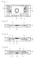
- an electronic device according to the invention comprises a metal wiring substrate 1, according to the Requirements is structured and links to his in Fig. 1 and right end portions connector 2 has.
- the Metal wiring support 1 can be made as for example Be executed copper existing stamped part, wherein tongue-shaped terminal contacts 3 of the connector 2 integral part of the punched wiring substrate 1 are.
- Fig. 1 are directly on the metal wiring carrier 1 electronic load switch 4 applied, for example, as unpacked nude chips can be executed.
- the electronic circuit breaker 4 are via suitable connecting lines with those through the Punching grid of the wiring substrate 1 given tracks connected.
- the circuit carrier 5 can be used as a printed circuit board, in particular flexible printed circuit board, hybrid ceramics, Multilayer ceramic such as LTCC ceramic or also be designed as an insulated metal substrate (IMS).
- the circuit carrier 5 may, for example, as a thin Flex PCB on the example as a copper connector leadframe formed wiring substrate 1 laminated become.
- an integrated circuit. 6 applied on the circuit substrate 5 is shown in the Embodiment an integrated circuit. 6 applied.
- the integrated circuit 6 is via suitable Tracks and connecting cables with the electronic Load switches 4 connected (not shown).
- Next to the Imaged integrated circuit 6 may also include others Parts of control electronics on the circuit carrier. 5 to be appropriate. It is essential, however, that the of the electronic circuit breakers 4 switched currents exclusively via the metal wiring carrier 1 flow, whereas the electronic circuit breaker. 4 switching control currents exclusively via interconnects the circuit carrier 5 or in corresponding Drive lines from the circuit carrier 5 to the Switches 4 flow.
- metal wiring carrier 1 together with the attached circuit breakers 4 and the circuit carrier 5 arranged thereon in a for example, from a thermosetting Umpressung bring existing housing.
- thermosetting Umpressung bring existing housing.
- thermoplastic encapsulation can be selected.
- a inventive electronic device for a Motor vehicle is on a level below the first Wiring carrier 1 a second metal Wiring carrier 7 is provided, each in the range of Connector 2 additional connection contacts 8 is formed.
- the in the lower plane in Fig. 3 level tracks of the second metal wiring substrate 7 become suitable locations as conductor track sections 9 up in the plane of the first metal wiring substrate or in the plane of the circuit carrier 5 transferred to a connection of as a performance or Control terminals running additional connection contacts 8 with the corresponding circuit breakers 4 and the to allow appropriate control electronics.
- Fig. 4 is an embodiment of an inventive electronic device, in which also two in arranged below each other levels metal Wiring carrier 1, 7 are provided.
- upper or first wiring substrate 1 are as already in the two embodiments described above electronic Load switch 4 applied.
- the upper wiring substrate. 1 together with the applied thereon switches 4 with a thermosetting Umdgurung 10 provided.
- the lower or second wiring support 7 is connected to a circuit carrier. 5 connected on which an integrated circuit 6 and optionally further not shown control logic is applied. Via suitable connecting lines 11 is the circuit carrier 5 with the load switch 4 bearing upper wiring substrate 1 connected.
- thermoset Umpressung 10 Another not pictured Circuit carrier with an additional control logic for the Load switch 4 to install.
Landscapes
- Engineering & Computer Science (AREA)
- Microelectronics & Electronic Packaging (AREA)
- Coupling Device And Connection With Printed Circuit (AREA)
- Control Of Direct Current Motors (AREA)
Description
- Fig. 1
- eine Draufsicht auf eine Ausführungsform eines erfindungsgemäßen elektronischen Gerätes;
- Fig. 2
- eine Seitenansicht der in Fig. 1 abgebildeten Ausführungsform;
- Fig. 3
- eine Seitenansicht einer weiteren Ausführungsform eines erfindungsgemäßen elektronischen Gerätes;
- Fig. 4
- eine Seitenansicht einer weiteren Ausführungsform eines erfindungsgemäßen elektronischen Gerätes.
Claims (10)
- Elektronisches Gerät für ein Kraftfahrzeug, umfassenddadurch gekennzeichnet, dass der metallene Verdrahtungsträger (1, 7) als Stanzgitter ausgeführt ist und Anschlussstecker (2) ausbildet, die gestanzte Anschlusskontakte (3, 8) umfassen.mindestens einen elektronischen Lastschalter (4), der auf einem metallenen Verdrahtungsträger (1, 7) aufgebracht ist,eine Elektronik, welche zumindest einen integrierten Schaltkreis (6) beinhaltet;einen mit dem metallenen Verdrahtungsträger (1, 7) verbundenen Schaltungsträger (5), auf dem die Elektronik angeordnet ist, wobei die Lastströme des mindestens einen elektronischen Lastschalters (4) über den metallenen Verdrahtungsträger (1, 7), nicht aber über den Schaltungsträger (5) geleitet sind;
- Elektronisches Gerät nach Anspruch 1, dadurch gekennzeichnet, daß der Schaltungsträger (5) als Leiterplatte ausgeführt ist.
- Elektronisches Gerät nach Anspruch 2, dadurch gekennzeichnet, daß der Schaltungsträger (5) als flexible Leiterplatte ausgeführt ist.
- Elektronisches Gerät nach Anspruch 1, dadurch gekennzeichnet, daß der Schaltungsträger als Hybridkeramik oder als Multilayerkeramik, insbesondere als LTCC-Keramik, ausgeführt ist.
- Elektronisches Gerät nach Anspruch 1, dadurch gekennzeichnet, daß der Schaltungsträger (5) als insulated metall substrate (IMS) ausgeführt ist.
- Elektronisches Gerät nach einem der Ansprüche 1 bis 5, dadurch gekennzeichnet, daß der metallene Verdrahtungsträger (1, 7) eine duroplastische Umpressung (10) aufweist, welche ein Gehäuse für den mindestens einen Lastschalter (4) des Gerätes ausbildet.
- Elektronisches Gerät nach einem der Ansprüche 1 bis 5, dadurch gekennzeichnet, daß der metallene Verdrahtungsträger (1, 7) eine duroplastische Umpressung oder thermoplastische Umspritzung aufweist, welche ein Gehäuse für den Verdrahtungsträger (1, 7) ausbildet.
- Elektronisches Gerät nach einem der Ansprüche 1 bis 7, dadurch gekennzeichnet, daß das Gerät mehrere metallene Verdrahtungsträger (1, 7) aufweist.
- Elektronisches Gerät nach Anspruch 8, dadurch gekennzeichnet, daß die metallenen Verdrahtungsträger (1, 7) in mehreren Ebenen angeordnet sind.
- Elektronisches Gerät nach einem der Ansprüche 8 oder 9, dadurch gekennzeichnet, daß der mindestens eine Lastschalter (4) und die Elektronik auf separaten Verdrahtungsträgern (1, 7) angeordnet sind.
Applications Claiming Priority (2)
| Application Number | Priority Date | Filing Date | Title |
|---|---|---|---|
| DE1999143258 DE19943258A1 (de) | 1999-09-10 | 1999-09-10 | Elektronisches Gerät für ein Kraftfahrzeug |
| DE19943258 | 1999-09-10 |
Publications (3)
| Publication Number | Publication Date |
|---|---|
| EP1083780A2 EP1083780A2 (de) | 2001-03-14 |
| EP1083780A3 EP1083780A3 (de) | 2003-09-03 |
| EP1083780B1 true EP1083780B1 (de) | 2005-11-16 |
Family
ID=7921455
Family Applications (1)
| Application Number | Title | Priority Date | Filing Date |
|---|---|---|---|
| EP20000119072 Expired - Lifetime EP1083780B1 (de) | 1999-09-10 | 2000-09-02 | Elektronisches Gerät für ein Kraftfahrzeug |
Country Status (2)
| Country | Link |
|---|---|
| EP (1) | EP1083780B1 (de) |
| DE (2) | DE19943258A1 (de) |
Cited By (1)
| Publication number | Priority date | Publication date | Assignee | Title |
|---|---|---|---|---|
| US8837150B2 (en) | 2009-09-15 | 2014-09-16 | Lisa Dräxlmaier GmbH | Electronic device for switching currents and method for producing the same |
Families Citing this family (1)
| Publication number | Priority date | Publication date | Assignee | Title |
|---|---|---|---|---|
| DE102008040290A1 (de) | 2008-07-09 | 2010-01-14 | Robert Bosch Gmbh | Hybridschaltungsstruktur mit keramischen Schaltungsträgern |
Family Cites Families (6)
| Publication number | Priority date | Publication date | Assignee | Title |
|---|---|---|---|---|
| DE69227066T2 (de) * | 1991-05-31 | 1999-06-10 | Denso Corp., Kariya, Aichi | Elektronische Vorrichtung |
| DE4244064C2 (de) * | 1992-12-24 | 1996-02-29 | Stribel Gmbh | Einrichtung für ein Fahrzeug |
| DE4419005A1 (de) * | 1994-05-31 | 1995-12-07 | Hella Kg Hueck & Co | Elektronischer Lastschalter für Kraftfahrzeuge |
| DE19522126C2 (de) * | 1995-06-19 | 1999-01-28 | Hella Kg Hueck & Co | Elektronischer Lastschalter für ein Kraftfahrzeug, beispielsweise Blinkgeber |
| DE19703304A1 (de) * | 1997-01-30 | 1998-08-06 | Telefunken Microelectron | Zentralelektronik |
| DE19727548A1 (de) * | 1997-06-28 | 1999-01-07 | Bosch Gmbh Robert | Elektronisches Steuergerät |
-
1999
- 1999-09-10 DE DE1999143258 patent/DE19943258A1/de not_active Withdrawn
-
2000
- 2000-09-02 EP EP20000119072 patent/EP1083780B1/de not_active Expired - Lifetime
- 2000-09-02 DE DE50011614T patent/DE50011614D1/de not_active Expired - Fee Related
Cited By (1)
| Publication number | Priority date | Publication date | Assignee | Title |
|---|---|---|---|---|
| US8837150B2 (en) | 2009-09-15 | 2014-09-16 | Lisa Dräxlmaier GmbH | Electronic device for switching currents and method for producing the same |
Also Published As
| Publication number | Publication date |
|---|---|
| EP1083780A2 (de) | 2001-03-14 |
| DE19943258A1 (de) | 2001-03-15 |
| DE50011614D1 (de) | 2005-12-22 |
| EP1083780A3 (de) | 2003-09-03 |
Similar Documents
| Publication | Publication Date | Title |
|---|---|---|
| DE60120813T2 (de) | Elektrischer Verbindungskasten für Kraftfahrzeuge | |
| DE19854180B4 (de) | Modulgehäuse für Halbleiterbauteile | |
| DE19939933B4 (de) | Elektronische Leistungs-Moduleinheit | |
| DE69532700T2 (de) | Steuerschaltungsmodul | |
| EP1083599B1 (de) | Leistungshalbleitermodul | |
| EP0368142B1 (de) | Elektronisches Steuergerät | |
| DE19645635C1 (de) | Steuergerät zur Ansteuerung des Elektromotors von Kraftfahrzeugen | |
| EP0935818B1 (de) | Elektronisches steuergerät | |
| DE10302372A1 (de) | Elektrisches Verbindergehäuse | |
| DE4031051C2 (de) | Modul mit mindestens einem Halbleiterschaltelement und einer Ansteuerschaltung | |
| DE69912657T2 (de) | Kraftfahrzeugschalterkasten | |
| EP3031308B1 (de) | Leiterplattenanordnung, steuervorrichtung für ein kühlerlüftermodul und verfahren | |
| EP0750452A1 (de) | Elektronischer Lastschalter für ein Kraftfahrzeug | |
| DE4335946A1 (de) | Anordnung bestehend aus einer Leiterplatte | |
| EP0685939A1 (de) | Elektronischer Lastschalter für Kraftfahrzeuge | |
| DE3527208A1 (de) | Elektrisches schaltgeraet | |
| DE102005014746A1 (de) | Aktive primärseitige Schaltungsanordnung für ein Schaltnetzteil | |
| EP1498947A2 (de) | Elektronische Schaltung mit einem Leistungshalbleiterbauelement und mit einem Sicherungsmittel zum Schutz des Leistungshalbleiterbauelements vor Überhitzung | |
| EP0696818A2 (de) | Halbleiterbauelement mit isolierendem Gehäuse | |
| DE60031199T2 (de) | Verbesserungen an elektrischen Schaltungen | |
| DE102013226513A1 (de) | Leiterplatte, Verfahren zum Herstellen derselben und Leiterplattenvorrichtung | |
| DE29819349U1 (de) | Halbleiter-Schaltungsanordnung, insbesondere Hochstromumrichter mit niedriger Zwischenkreisspannung | |
| DE19943258A1 (de) | Elektronisches Gerät für ein Kraftfahrzeug | |
| DE112019005172T5 (de) | Schaltungsbaugruppe und elektrische Anschlussdose | |
| DE102005048097A1 (de) | Steuergeräteanordnung |
Legal Events
| Date | Code | Title | Description |
|---|---|---|---|
| PUAI | Public reference made under article 153(3) epc to a published international application that has entered the european phase |
Free format text: ORIGINAL CODE: 0009012 |
|
| AK | Designated contracting states |
Kind code of ref document: A2 Designated state(s): AT BE CH CY DE DK ES FI FR GB GR IE IT LI LU MC NL PT SE |
|
| AX | Request for extension of the european patent |
Free format text: AL;LT;LV;MK;RO;SI |
|
| PUAL | Search report despatched |
Free format text: ORIGINAL CODE: 0009013 |
|
| AK | Designated contracting states |
Kind code of ref document: A3 Designated state(s): AT BE CH CY DE DK ES FI FR GB GR IE IT LI LU MC NL PT SE |
|
| AX | Request for extension of the european patent |
Extension state: AL LT LV MK RO SI |
|
| RIC1 | Information provided on ipc code assigned before grant |
Ipc: 7H 05K 5/00 A Ipc: 7B 60R 16/02 B |
|
| 17P | Request for examination filed |
Effective date: 20040205 |
|
| 17Q | First examination report despatched |
Effective date: 20040317 |
|
| AKX | Designation fees paid |
Designated state(s): DE ES FR GB IT |
|
| RAP1 | Party data changed (applicant data changed or rights of an application transferred) |
Owner name: HELLA KGAA HUECK & CO. |
|
| RTI1 | Title (correction) |
Free format text: ELECTRONIC DEVICE FOR A MOTOR VEHICLE |
|
| GRAP | Despatch of communication of intention to grant a patent |
Free format text: ORIGINAL CODE: EPIDOSNIGR1 |
|
| GRAS | Grant fee paid |
Free format text: ORIGINAL CODE: EPIDOSNIGR3 |
|
| GRAA | (expected) grant |
Free format text: ORIGINAL CODE: 0009210 |
|
| AK | Designated contracting states |
Kind code of ref document: B1 Designated state(s): DE ES FR GB IT |
|
| PG25 | Lapsed in a contracting state [announced via postgrant information from national office to epo] |
Ref country code: IT Free format text: LAPSE BECAUSE OF FAILURE TO SUBMIT A TRANSLATION OF THE DESCRIPTION OR TO PAY THE FEE WITHIN THE PRESCRIBED TIME-LIMIT;WARNING: LAPSES OF ITALIAN PATENTS WITH EFFECTIVE DATE BEFORE 2007 MAY HAVE OCCURRED AT ANY TIME BEFORE 2007. THE CORRECT EFFECTIVE DATE MAY BE DIFFERENT FROM THE ONE RECORDED. Effective date: 20051116 Ref country code: GB Free format text: LAPSE BECAUSE OF FAILURE TO SUBMIT A TRANSLATION OF THE DESCRIPTION OR TO PAY THE FEE WITHIN THE PRESCRIBED TIME-LIMIT Effective date: 20051116 |
|
| REG | Reference to a national code |
Ref country code: GB Ref legal event code: FG4D Free format text: NOT ENGLISH |
|
| REF | Corresponds to: |
Ref document number: 50011614 Country of ref document: DE Date of ref document: 20051222 Kind code of ref document: P |
|
| PG25 | Lapsed in a contracting state [announced via postgrant information from national office to epo] |
Ref country code: ES Free format text: LAPSE BECAUSE OF FAILURE TO SUBMIT A TRANSLATION OF THE DESCRIPTION OR TO PAY THE FEE WITHIN THE PRESCRIBED TIME-LIMIT Effective date: 20060227 |
|
| GBV | Gb: ep patent (uk) treated as always having been void in accordance with gb section 77(7)/1977 [no translation filed] |
Effective date: 20051116 |
|
| ET | Fr: translation filed | ||
| PGFP | Annual fee paid to national office [announced via postgrant information from national office to epo] |
Ref country code: FR Payment date: 20060908 Year of fee payment: 7 |
|
| PLBE | No opposition filed within time limit |
Free format text: ORIGINAL CODE: 0009261 |
|
| STAA | Information on the status of an ep patent application or granted ep patent |
Free format text: STATUS: NO OPPOSITION FILED WITHIN TIME LIMIT |
|
| 26N | No opposition filed |
Effective date: 20060817 |
|
| REG | Reference to a national code |
Ref country code: FR Ref legal event code: ST Effective date: 20080531 |
|
| PG25 | Lapsed in a contracting state [announced via postgrant information from national office to epo] |
Ref country code: FR Free format text: LAPSE BECAUSE OF NON-PAYMENT OF DUE FEES Effective date: 20071001 |
|
| PGFP | Annual fee paid to national office [announced via postgrant information from national office to epo] |
Ref country code: DE Payment date: 20080919 Year of fee payment: 9 |
|
| PG25 | Lapsed in a contracting state [announced via postgrant information from national office to epo] |
Ref country code: DE Free format text: LAPSE BECAUSE OF NON-PAYMENT OF DUE FEES Effective date: 20100401 |