EP1083661A2 - Noise shaping dynamic element matching in analog to digital converters - Google Patents
Noise shaping dynamic element matching in analog to digital converters Download PDFInfo
- Publication number
- EP1083661A2 EP1083661A2 EP00119317A EP00119317A EP1083661A2 EP 1083661 A2 EP1083661 A2 EP 1083661A2 EP 00119317 A EP00119317 A EP 00119317A EP 00119317 A EP00119317 A EP 00119317A EP 1083661 A2 EP1083661 A2 EP 1083661A2
- Authority
- EP
- European Patent Office
- Prior art keywords
- capacitors
- group
- sub
- sample period
- digital output
- Prior art date
- Legal status (The legal status is an assumption and is not a legal conclusion. Google has not performed a legal analysis and makes no representation as to the accuracy of the status listed.)
- Withdrawn
Links
Images



Classifications
-
- H—ELECTRICITY
- H03—ELECTRONIC CIRCUITRY
- H03M—CODING; DECODING; CODE CONVERSION IN GENERAL
- H03M1/00—Analogue/digital conversion; Digital/analogue conversion
- H03M1/12—Analogue/digital converters
- H03M1/34—Analogue value compared with reference values
-
- H—ELECTRICITY
- H03—ELECTRONIC CIRCUITRY
- H03M—CODING; DECODING; CODE CONVERSION IN GENERAL
- H03M1/00—Analogue/digital conversion; Digital/analogue conversion
- H03M1/06—Continuously compensating for, or preventing, undesired influence of physical parameters
- H03M1/0617—Continuously compensating for, or preventing, undesired influence of physical parameters characterised by the use of methods or means not specific to a particular type of detrimental influence
- H03M1/0634—Continuously compensating for, or preventing, undesired influence of physical parameters characterised by the use of methods or means not specific to a particular type of detrimental influence by averaging out the errors, e.g. using sliding scale
- H03M1/0656—Continuously compensating for, or preventing, undesired influence of physical parameters characterised by the use of methods or means not specific to a particular type of detrimental influence by averaging out the errors, e.g. using sliding scale in the time domain, e.g. using intended jitter as a dither signal
- H03M1/066—Continuously compensating for, or preventing, undesired influence of physical parameters characterised by the use of methods or means not specific to a particular type of detrimental influence by averaging out the errors, e.g. using sliding scale in the time domain, e.g. using intended jitter as a dither signal by continuously permuting the elements used, i.e. dynamic element matching
- H03M1/0665—Continuously compensating for, or preventing, undesired influence of physical parameters characterised by the use of methods or means not specific to a particular type of detrimental influence by averaging out the errors, e.g. using sliding scale in the time domain, e.g. using intended jitter as a dither signal by continuously permuting the elements used, i.e. dynamic element matching using data dependent selection of the elements, e.g. data weighted averaging
- H03M1/0668—Continuously compensating for, or preventing, undesired influence of physical parameters characterised by the use of methods or means not specific to a particular type of detrimental influence by averaging out the errors, e.g. using sliding scale in the time domain, e.g. using intended jitter as a dither signal by continuously permuting the elements used, i.e. dynamic element matching using data dependent selection of the elements, e.g. data weighted averaging the selection being based on the output of noise shaping circuits for each element
-
- H—ELECTRICITY
- H03—ELECTRONIC CIRCUITRY
- H03M—CODING; DECODING; CODE CONVERSION IN GENERAL
- H03M1/00—Analogue/digital conversion; Digital/analogue conversion
- H03M1/12—Analogue/digital converters
- H03M1/14—Conversion in steps with each step involving the same or a different conversion means and delivering more than one bit
- H03M1/16—Conversion in steps with each step involving the same or a different conversion means and delivering more than one bit with scale factor modification, i.e. by changing the amplification between the steps
- H03M1/164—Conversion in steps with each step involving the same or a different conversion means and delivering more than one bit with scale factor modification, i.e. by changing the amplification between the steps the steps being performed sequentially in series-connected stages
- H03M1/167—Conversion in steps with each step involving the same or a different conversion means and delivering more than one bit with scale factor modification, i.e. by changing the amplification between the steps the steps being performed sequentially in series-connected stages all stages comprising simultaneous converters
- H03M1/168—Conversion in steps with each step involving the same or a different conversion means and delivering more than one bit with scale factor modification, i.e. by changing the amplification between the steps the steps being performed sequentially in series-connected stages all stages comprising simultaneous converters and delivering the same number of bits
Definitions
- a first residual signal V RES1 is provided on line 24 from stage one 12 to stage two 14.
- a second residual signal V RES2 is provided on line 26 from stage two 14 to stage three 16.
- a third residual signal V RES3 is provided on line 28 from stage three 16 to stage four 18.
- a further residual signal is provided from stage four 18 on line 30, and so forth.
- stage two 14 the functional components of stage two 14 are shown by way of example.
- input line 24 can be seen, which is an input to sample and hold amplifier (“SHA") 32.
- the output of SHA 32 is provided on line 34 to an m-bit analog-to-digital subconverter (ADSC) 36, which is typically a flash ADC, and to a first input of a summing unit 38.
- ADSC analog-to-digital subconverter
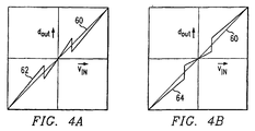
- Figs. 4a and 4b show a consequence of this approach.
- Fig. 4a and Fig. 4b are graphs of the input voltage versus the output voltage of the sample and hold amplifier of Figs. 2 and 3, i.e., the effective transfer curve of that unit, for two cases.
- a curve 62 is shown for the transfer curve in the case where C1 ⁇ C2.
- a curve 64 is shown for the transfer curve in the case where C1 > C2.
- the ideal transfer curve is shown by a line 60 in both Fig. 4a and Fig. 4b.
- the value of C1 vs. C2 is fixed once the chip is fabricated. Therefore, in operation the ADC will have a transfer curve like curve 62, or curve 64, all the time.
- capacitor shuffling is accomplished that provides a noise shaped element mismatch.
- the capacitor shuffling of the present invention noise shapes interstage gain error.
- Fig. 5 is a circuit diagram of pertinent portions of an ADC stage, shown in the sampling phase, for use in accordance with a preferred embodiment of method of the present invention.
- a comparator generating a value d used to generate an m-bit sub-word is omitted from the diagram, in the interest of brevity, but it will be understood that such component exists in actual implementations.
- a differential amplifier 70 having a non-inverting input connected to ground by way of a line 72.
- switch S S ' provides a virtual ground connection for capacitors C11, C12, ..., C1q, and capacitors C21, C22, ..., C2p, so that they can charge up during the sample phase, and capture the sampled voltage V IN at the sample time.
- switch S S ' is opened at the end of the sample phase to capture that charge for use in the next, amplifying phase.
- Fig. 6 is a circuit diagram of the circuit of Fig. 5, as configured in a second phase, that of amplification.
- the capacitors in the first group, C11, C12, ... C1q are now connected all in parallel as feedback capacitors between the output line 76 and the inverting input of amplifier 70.
- the capacitors in the second group, C21, C22, ... C2p are now all connected in parallel together as DASC capacitors between the negative input of amplifier 70 and to a respective one of a corresponding number of switches S1, S2, ... Sp.
- Each of these switches, S1, S2, ... Sp allows the port of its respective DASC capacitor to be connected to V REF , ground, or ⁇ V REF , depending upon the position of the switch, which, again is determined by the value d output by the comparator (not shown).
- the connection of the DASC capacitors are fixed once the digital code from the ADSC is determined.
- the feedback capacitor is usually predetermined to be C11 for all time.
- the connections of the DASC capacitors to V REF , GND, and -V REF are shuffled by a procedure that provides a noise shaped element mismatch, and a noise shaped interstage gain error.
- the numbers p and q are selectable, depending upon the performance desired versus the chip area to be occupied by the sample and hold amplifier. Out of the p number of unit capacitors, depending on the digital decisions, a selectable number i of them may be connected to V REF , j of them to -V REF , and k of them to GND. Over time, however, part or all of the q feedback capacitors may be used as the DASC capacitor, and vice versa.
- the number of bits per stage is three.
- One conventional architecture uses four capacitors per stage, with p being three and q being one.
- the three DASC capacitors are C21, C22 and C23, which are denominated C2, C3 and C4 in the discussion that follows, while C11 is the feedback capacitor, which is denominated C1 in the discussion that follows.
- the analog input is such that the ADSC output is two.
- C2 as part of the DASC capacitors, is always selected to connect to -V REF , while C3 and C4 are connected to GND.
- C1 through C4 are selected according to the aforementioned shuffling procedure to connect to -V REF .
- the two connections to GND and the feedback capacitor are all chosen by the procedure as well.
- the harmonic distortion usually associated with capacitor mismatch is converted into noise that may have its spectral amplitude shaped so as to have a peak, or maximum, that may be placed substantially outside of the band of interest for the particular application.
- a methodology is provided that causes an individual level averaging type noise shaping.
- the switching of switches S1, S2, ... S7 is controlled in dependence on the digital output of the m-bit ADSC 36, on line 40 (Fig. 1) for the previous sample time.
- FIGs. 7 through 15 are block diagrams of pertinent portions of arrangements in which these methods are practiced.
- the block diagrams include elements U, such as capacitors, that are shuffled in accordance with these methods. Also included in these block diagrams are registers R where values are stored that are used to determine the particular pattern of shuffling. Summing nodes are also included.
- These block diagrams are generalized arrangements, and can, for example, be applied to specific types of arrangements such as that shown in Fig. 5 and Fig. 6, in which case the elements shuffled are the capacitors described hereinabove in connection with those figures.
- a digital input line 40 carrying the digital output of the m-bit ADSC 36 for a sample period.
- the digital value on line 40 is used to select the arrangement of capacitors for the sample and hold amplifier 32 in the next following hold, or amplification phase as follows.
- Each of the registers in the register set 102 stores a value pointing to an element in a stack of elements 104, identified by a cyclic sequence from one to nine, being cyclic in that as selections are made of these elements in the selection procedure, after the ninth element is selected in a sequence, the procedure simply wraps to the first element and continues.
- the stack of elements 104 thus comprises elements U1, U2, ... U9, as shown.
- Each of the elements in element stack 104 corresponds to one of the capacitors C1, C2, ... C9, on a one-to-one basis.
- element U1 corresponds to capacitor C1
- element U2 corresponds to capacitor C2, and so forth.
- the element pointed to by the selected register is used in a decision about which switches to set in the present hold phase.
- Elements U4, U5 and U6, which follow U3 in the sequence, are automatically selected such that their corresponding capacitors C4, C5 and C6 are used as the DASC capacitors connecting to V REF during the hold phase.
- the remaining capacitors C7, C8, C9 and C1 are automatically selected and switched to connect to ⁇ V REF during the hold phase.
- the analog output A OUT is the conceptual output voltage of the DASC of the stage, i.e., the output 44 of the m-bit DASC 42 of Fig. 1, when the capacitors are configured in this way. This is true for all of the figures described below, as well.
- a stack of elements 110 is provided, comprising elements U1, U2, ... U9, as shown, wherein each of the elements in element stack 110 corresponds to one of the capacitors C1, C2, ... C9, on a one to one basis.
- this method only one register 112 is provided to receive the digital input d in on line 40.
- the digital value stored in register 112 points, as a result of earlier decisions, to U2, the first element in the stack 110 to be used to represent the DAC level.
- the element pointed to by the selected register is used in a decision about which switches to set in the present hold phase. Specifically, the switches corresponding to the element pointed to, and the next element in the stack 110, U2 and U3, are switched such that their corresponding capacitors are selected as the feedback capacitors. Since d in is three in this example, the switches corresponding to the next three elements in the stack 110, U4, U5 and U6, are switched such that their corresponding capacitors are selected as the DASC capacitors, connecting to V REF during the hold phase. The remaining capacitors, C7, C8, C9 and C1 are connected to ⁇ V REF during the hold phase. Register 112 is updated in the same sample period such that the element pointer is increased by a number equal to the sum of the number of feedback capacitors and the number of DASC capacitors, in this case to U7. Capacitor usage rotates accordingly.
- the contents of the register points to an element in the stack 122 of elements.
- a single pointer is used to point to the next feedback element to be used.
- the first DAC capacitor is the one that immediately follows the feedback capacitors.
- these techniques were to be applied to the 1.5b/stage architecture shown in Fig. 2, the feedback capacitor would never change, leaving the interstage gain error not averaged. For this reason, further methodologies are described herein, beginning with this fourth methodology.
- the basic concept is to have different pointers for the feedback and for the DAC capacitors.
- each register since each register stores two values, it may be desired to initially have the feedback pointers of R1 through R9 point to U1, while the DAC pointers of R1 through R9 point to U3. Again, the user may decide on a different initialization pattern, as desired, the particular initialization pattern not being critical to the invention.
- a single register 148 is used.
- d in 3.
- This technique is similar in some respects to the second embodiment, described above, except that two pointers are used.
- the current DAC pointer is pointing at U2
- the current feedback capacitor pointer is pointing at U7.
- capacitors C7 and C8 are the feedback capacitors.
- the DAC and feedback pointers are updated to U5 and U9, respectively.
- circuits shown in Figures 2, 3, 5 and 6 are single ended, for ease of explanation.
- the principles are the same for circuits that are fully differential, and the considerations involved in implementing the present invention are essentially the same as those discussed herein, with the considerations applying to both differential paths, rather than to only the one path in a single-ended circuit.
Landscapes
- Engineering & Computer Science (AREA)
- Theoretical Computer Science (AREA)
- Analogue/Digital Conversion (AREA)
- Compression, Expansion, Code Conversion, And Decoders (AREA)
Abstract
Description
Claims (10)
- A method for shuffling capacitors from sample period to sample period in a stage of a multi-stage analog to digital converter ("ADC"), the ADC stage receiving for each sample period an input having a first analog voltage level, and providing for each sample period a digital output representing a second voltage level corresponding to said first analog voltage level to a predetermined digital accuracy and providing an analog output representative of the difference between said first analog voltage level and a second analog voltage level corresponding to said digital output, said ADC stage including a plurality of capacitors usable for storage of charge during a sample phase and for providing during an amplification phase, in conjunction with an amplifier, an output signal having a voltage representing the difference between said second analog voltage level and said first analog voltage level, comprising the steps of:providing said input to said plurality of capacitors during said sample phase to capture and hold said first analog voltage level at a first time in said sample phase;using a selected sub-group of said plurality of capacitors as feedback capacitors and using a remaining sub-group of said plurality of capacitors as digital to analog subconverter ("DASC") capacitors, said selected sub-group and said remaining sub-group being different sets in adjacent sample periods, in conjunction with said amplifier, in accordance with a predetermined capacitor shuffling procedure adapted to convert resulting harmonic distortion associated with capacitor mismatch into noise having a spectral amplitude peak placed outside of a predetermined spectral band.
- A method in accordance with Claim 1, wherein said predetermined capacitor shuffling procedure comprises the following steps:uniquely identifying each capacitor in said plurality of capacitors in a cyclic sequence;for a first sample period,using said digital output for said first sample period to select, based on a first stored selection associated with the value of said digital output for said first sample period, a first sub-group of said plurality of capacitors, contiguous in said sequence, as said selected sub-group and using said first sub-group as feedback capacitors,using a second sub-group of capacitors, immediately following said first sub-group of feedback capacitors in said sequence as said remaining sub-group as DASC capacitors, the number of capacitors in said second sub-group being determined by said digital output for said first sample period;updating said first stored selection associated with the value of said digital output for said first sample period to the next capacitor in said sequence after the last of said sub-group of capacitors; andfor a subsequent sample period,using said digital output for said subsequent sample period to select, based on a second stored selection associated with the value of said digital output for said subsequent sample period, a third sub-group of said plurality of capacitors, contiguous in said sequence, as said selected sub-group and using said third sub-group as feedback capacitors,using a fourth sub-group of capacitors, immediately following said third sub-group of feedback capacitors in said sequence as said remaining sub-group as DASC capacitors, the number of capacitors in said third sub-group being determined by said digital output for said subsequent sample period; andupdating said second stored selection associated with the value of said digital output for said subsequent sample period to the next capacitor in said sequence after the last of said fourth sub-group of capacitors.
- A method in accordance with Claim 1, wherein said predetermined capacitor shuffling procedure comprises the following steps:uniquely identifying each capacitor in said plurality of capacitors in a cyclic sequence;for a first sample period,selecting, based on a stored selection, a first sub-group of said plurality of capacitors, contiguous in said sequence, as said selected sub-group and using said first sub-group as feedback capacitors,using a second sub-group of capacitors, immediately following said first sub-group of feedback capacitors in said sequence as said remaining sub-group as DASC capacitors, the number of capacitors in said second sub-group being determined by said digital output for said first sample period, and using said second sub-group of capacitors as DASC capacitors, andupdating said stored selection to the next capacitor in said sequence after the last of said sub-group of capacitors; andfor a subsequent sample period,selecting, based on said stored selection, a third sub-group of said plurality of capacitors, contiguous in said sequence, as said selected sub-group and using said third sub-group as feedback capacitors,using a fourth sub-group of capacitors, immediately following said third sub-group of feedback capacitors in said sequence as said remaining sub-group as DASC capacitors, the number of capacitors in said third sub-group being determined by said digital output for said subsequent sample period, and using said fourth sub-group of capacitors as DASC capacitors, andupdating said stored selection to the next capacitor in said sequence after the last of said fourth sub-group of capacitors.
- A method in accordance with Claim 1, wherein said predetermined capacitor shuffling procedure comprises the following steps:uniquely identifying each capacitor in said plurality of capacitors in a cyclic sequence;for a first sample period,using said digital output for said first sample period to select, based on a first stored selection associated with a first group of values of said digital output including the value for said first sample period, a first sub-group of said plurality of capacitors, contiguous in said sequence, as said selected sub-group and using said first sub-group as feedback capacitors,using a second sub-group of capacitors, immediately following said first sub-group of feedback capacitors in said sequence as said remaining sub-group as DASC capacitors, the number of capacitors in said second sub-group being determined by said digital output for said first sample period, andupdating said first stored selection associated with said group of values of said digital output including the value of said digital output for said first sample period to the next capacitor in said sequence after the last of said sub-group of capacitors; andfor a subsequent sample period,using said digital output for said subsequent sample period to select, based on a second stored selection associated with a second group of values of said digital output including the value of said digital output for said subsequent sample period, a third sub-group of said plurality of capacitors, contiguous in said sequence, as said selected sub-group and using said third sub-group as feedback capacitors,using a fourth sub-group of capacitors, immediately following said third sub-group of feedback capacitors in said sequence as said remaining sub-group as DASC capacitors, the number of capacitors in said third sub-group being determined by said digital output for said subsequent sample period, andupdating said second stored selection associated with said second group of values of said digital output including the value of said digital output for said subsequent sample period to the next capacitor in said sequence after the last of said fourth sub-group of capacitors.
- A method in accordance with Claim 1, wherein said predetermined capacitor shuffling procedure comprises the following steps:for a first sample period,using said digital output for said first sample period to select, based on a first stored selection associated with the value of said digital output for said first sample period, a first sub-group of said plurality of capacitors, contiguous in said sequence, as said selected sub-group and using said first sub-group as feedback capacitors,using said digital output for said first sample period to select, based on a second stored selection associated with the value of said digital output for said first sample period, a second sub-group of capacitors in said sequence as said remaining sub-group as DASC capacitors, the number of capacitors in said second sub-group being determined by said digital output for said first sample period,updating said first stored selection associated with the value of said digital output for said first sample period to the next capacitor in said sequence after the last of said first sub-group of capacitors, andupdating said second stored selection associated with the value of said digital output for said first sample period to the next capacitor in said sequence after the last of said second sub-group of capacitors; andfor a subsequent sample period,using said digital output for said subsequent sample period to select, based on a third stored selection associated with the value of said digital output for said subsequent sample period, a third sub-group of said plurality of capacitors, contiguous in said sequence, as said selected sub-group and using said third sub-group as feedback capacitors,using said digital output for said subsequent sample period to select, based on a second stored selection associated with the value of said digital output for said first sample period, a fourth sub-group of capacitors in said sequence as said remaining sub-group as DASC capacitors, the number of capacitors in said fourth sub-group being determined by said digital output for said subsequent sample period,updating said third stored selection associated with the value of said digital output for said subsequent sample period to the next capacitor in said sequence after the last of said third sub-group of capacitors, andupdating said fourth stored selection associated with the value of said digital output for said subsequent sample period to the next capacitor in said sequence after the last of said fourth sub-group of capacitors.
- A method in accordance with Claim 5, wherein, in the selection of capacitors for a sub-group during any sample period, the capacitors selected for use as feedback capacitors have priority over capacitors selected for use as DASC capacitors, such that, when selection conflict exists, capacitors in said sequence following capacitors selected for use as feedback capacitors are selected for DASC capacitors subject to said conflict.
- A method in accordance with Claim 1, wherein said predetermined capacitor shuffling procedure comprises the following steps:for a first sample period,selecting, based on a first stored selection, a first sub-group of said plurality of capacitors, contiguous in said sequence, as said selected sub-group and using said first sub-group as feedback capacitors,selecting, based on a second stored selection, a second sub-group of capacitors as DASC capacitors, the number of capacitors in said second sub-group being determined by said digital output for said first sample period,updating said first stored selection to the next capacitor in said sequence after the last of said first sub-group of capacitors,updating said second stored selection to the next capacitor in said sequence after the last of said second sub-group of capacitors; andfor a subsequent sample period,selecting, based on said first stored selection, a third sub-group of said plurality of capacitors, contiguous in said sequence, as said selected sub-group and using said third sub-group as feedback capacitors,selecting, based on said second stored selection, a fourth sub-group of capacitors as DASC capacitors, the number of capacitors in said fourth sub-group being determined by said digital output for said subsequent sample period,updating said first stored selection to the next capacitor in said sequence after the last of said third sub-group of capacitors, andupdating said second stored selection to the next capacitor in said sequence after the last of said fourth sub-group of capacitors.
- A method in accordance with Claim 7, wherein, in the selection of capacitors for a sub-group during any sample period, the capacitors selected for use as feedback capacitors have priority over capacitors selected for use as DASC capacitors, such that, when selection conflict exists, capacitors in said sequence following capacitors selected for use as feedback capacitors are selected for DASC capacitors subject to said conflict.
- A method in accordance with Claim 1, wherein said predetermined capacitor shuffling procedure comprises the following steps:uniquely identifying each capacitor in said plurality of capacitors in a cyclic sequence;for a first sample period,using said digital output for said first sample period to select, based on a first stored selection associated with a first group of values of said digital output including the value for said first sample period, a first sub-group of said plurality of capacitors, contiguous in said sequence, as said selected sub-group and using said first sub-group as feedback capacitors,using said digital output for said first sample period to select, based on a second stored selection associated with said first group of values of said digital output including the value for said first sample period, a second sub-group of capacitors as said remaining sub-group as DASC capacitors, the number of capacitors in said second sub-group being determined by said digital output for said first sample period, and using said second sub-group of capacitors as DASC capacitors,updating said first stored selection associated with said group of values of said digital output including the value of said digital output for said first sample period to the next capacitor in said sequence after the last of said first sub-group of capacitors, andupdating said second stored selection associated with said group of values of said digital output including the value of said digital output for said first sample period to the next capacitor in said sequence after the last of said second sub-group of capacitors; andfor a subsequent sample period,using said digital output for said subsequent sample period to select, based on a second stored selection associated with a second group of values of said digital output including the value for said subsequent sample period, a third sub-group of said plurality of capacitors, contiguous in said sequence, as said selected sub-group and using said third sub-group as feedback capacitors,using said digital output for said subsequent sample period to select, based on a fourth stored selection associated with said second group of values of said digital output including the value for said subsequent sample period, a fourth sub-group of capacitors as said remaining sub-group as DASC capacitors, the number of capacitors in said fourth sub-group being determined by said digital output for said subsequent sample period, and using said fourth sub-group of capacitors as DASC capacitors,updating said third stored selection associated with said group of values of said digital output including the value of said digital output for said subsequent sample period to the next capacitor in said sequence after the last of said third sub-group of capacitors, andupdating said fourth stored selection associated with said group of values of said digital output including the value of said digital output for said subsequent sample period to the next capacitor in said sequence after the last of said fourth sub-group of capacitors.
- A method in accordance with Claim 9, wherein, in the selection of capacitors for a sub-group during any sample period, the capacitors selected for use as feedback capacitors have priority over capacitors selected for use as DASC capacitors, such that, when selection conflict exists, capacitors in said sequence following capacitors selected for use as feedback capacitors are selected for DASC capacitors subject to said conflict.
Applications Claiming Priority (2)
| Application Number | Priority Date | Filing Date | Title |
|---|---|---|---|
| US09/392,138 US6211805B1 (en) | 1999-09-08 | 1999-09-08 | Noise shaping dynamic element mismatch in analog to digital converters |
| US392138 | 1999-09-08 |
Publications (2)
| Publication Number | Publication Date |
|---|---|
| EP1083661A2 true EP1083661A2 (en) | 2001-03-14 |
| EP1083661A3 EP1083661A3 (en) | 2003-09-03 |
Family
ID=23549396
Family Applications (1)
| Application Number | Title | Priority Date | Filing Date |
|---|---|---|---|
| EP00119317A Withdrawn EP1083661A3 (en) | 1999-09-08 | 2000-09-06 | Noise shaping dynamic element matching in analog to digital converters |
Country Status (5)
| Country | Link |
|---|---|
| US (1) | US6211805B1 (en) |
| EP (1) | EP1083661A3 (en) |
| JP (1) | JP2001102926A (en) |
| KR (1) | KR100730277B1 (en) |
| TW (1) | TW494641B (en) |
Cited By (1)
| Publication number | Priority date | Publication date | Assignee | Title |
|---|---|---|---|---|
| CN114050828A (en) * | 2022-01-07 | 2022-02-15 | 武汉杰开科技有限公司 | Digital-to-analog converter, mismatch calibration method of digital-to-analog converter and chip |
Families Citing this family (13)
| Publication number | Priority date | Publication date | Assignee | Title |
|---|---|---|---|---|
| US6885326B2 (en) * | 1999-02-04 | 2005-04-26 | Med-El Elektromedizinische Geraeta Gmbh | Accumulator for adaptive Σ-Δ modulation |
| JP4583689B2 (en) * | 1999-10-27 | 2010-11-17 | エヌエックスピー ビー ヴィ | Digital-to-analog converter |
| WO2001067614A1 (en) * | 2000-02-22 | 2001-09-13 | The Regents Of The University Of California | Digital cancellation of d/a converter noise in pipelined a/d converters |
| US6346898B1 (en) * | 2000-08-07 | 2002-02-12 | Audio Logic, Inc. | Multilevel analog to digital data converter having dynamic element matching in a reference data path |
| IT1320694B1 (en) * | 2000-10-06 | 2003-12-10 | St Microelectronics Srl | DYNAMIC EQUALIZATION METHOD OF THE ELEMENTS OF A DIGITAL / ANALOG MULTIBIT CONVERTER INTEGRATED WITH BALANCED OUTPUT FOR |
| US6617992B2 (en) | 2001-08-15 | 2003-09-09 | National Semiconductor Corporation | Capacitor mismatch independent gain stage for differential pipeline analog to digital converters |
| US6600440B1 (en) | 2001-08-15 | 2003-07-29 | National Semiconductor Corporation | Capacitor mismatch independent gain stage for pipeline analog to digital converters |
| KR100500440B1 (en) * | 2002-10-15 | 2005-07-12 | 삼성전자주식회사 | Multi-stage analog to digital converter with pipeline structure and coding method for designing it |
| US7193548B2 (en) * | 2004-01-30 | 2007-03-20 | Hrl Laboratories, Llc | Switching arrangement and DAC mismatch shaper using the same |
| US7187310B2 (en) * | 2005-03-04 | 2007-03-06 | Kamal El-Sankary | Circuit calibration using voltage injection |
| TWI304686B (en) * | 2006-01-06 | 2008-12-21 | Realtek Semiconductor Corp | Pipeline analog-to-digital converter capable of sharing comparators |
| US10003348B2 (en) * | 2016-09-08 | 2018-06-19 | Mediatek Inc. | Analog-to-digital converter with noise shaping |
| US12451895B2 (en) | 2022-10-28 | 2025-10-21 | Kepler Computing Inc. | Mismatch shaping apparatus and method for binary coded digital-to-analog converters |
Family Cites Families (5)
| Publication number | Priority date | Publication date | Assignee | Title |
|---|---|---|---|---|
| GB9224238D0 (en) | 1992-11-19 | 1993-01-06 | Vlsi Technology Inc | Pipelined analog to digital converters and interstage amplifiers for such converters |
| US5412387A (en) | 1993-04-06 | 1995-05-02 | Analog Devices, Inc. | Error reduction in switched capacitor digital-to-analog converter systems by balanced sampling |
| US5404142A (en) | 1993-08-05 | 1995-04-04 | Analog Devices, Incorporated | Data-directed scrambler for multi-bit noise shaping D/A converters |
| US5416485A (en) | 1993-12-20 | 1995-05-16 | Lee; Hae-Seung | Analog-to-digital conversion circuit with improved differential linearity |
| US6031480A (en) * | 1997-11-04 | 2000-02-29 | Texas Instruments Incorporated | Method and apparatus for implementing a pipelined A/D converter with inter-stage amplifiers having no common mode feedback circuitry |
-
1999
- 1999-09-08 US US09/392,138 patent/US6211805B1/en not_active Expired - Lifetime
-
2000
- 2000-09-06 EP EP00119317A patent/EP1083661A3/en not_active Withdrawn
- 2000-09-07 JP JP2000271419A patent/JP2001102926A/en not_active Abandoned
- 2000-09-08 KR KR1020000053292A patent/KR100730277B1/en not_active Expired - Fee Related
- 2000-09-26 TW TW089118385A patent/TW494641B/en not_active IP Right Cessation
Cited By (2)
| Publication number | Priority date | Publication date | Assignee | Title |
|---|---|---|---|---|
| CN114050828A (en) * | 2022-01-07 | 2022-02-15 | 武汉杰开科技有限公司 | Digital-to-analog converter, mismatch calibration method of digital-to-analog converter and chip |
| CN114050828B (en) * | 2022-01-07 | 2022-04-12 | 武汉杰开科技有限公司 | Digital-to-analog converter, mismatch calibration method of digital-to-analog converter and chip |
Also Published As
| Publication number | Publication date |
|---|---|
| KR20010030325A (en) | 2001-04-16 |
| KR100730277B1 (en) | 2007-06-19 |
| US6211805B1 (en) | 2001-04-03 |
| TW494641B (en) | 2002-07-11 |
| EP1083661A3 (en) | 2003-09-03 |
| JP2001102926A (en) | 2001-04-13 |
Similar Documents
| Publication | Publication Date | Title |
|---|---|---|
| US6784814B1 (en) | Correction for pipelined analog to digital (A/D) converter | |
| US5406283A (en) | Multi-bit oversampled DAC with dynamic element matching | |
| US10103742B1 (en) | Multi-stage hybrid analog-to-digital converter | |
| US7893859B2 (en) | Converter circuit, analog/digital converter, and method for generating digital signals corresponding to analog signals | |
| US6211805B1 (en) | Noise shaping dynamic element mismatch in analog to digital converters | |
| US6556158B2 (en) | Residue-compensating A/D converter | |
| US6486807B2 (en) | A/D converter calibration | |
| US6404364B1 (en) | Multistage converter employing digital dither | |
| US6028546A (en) | Pipeline analog-to-digital conversion that reduces the accumulation offset errors | |
| EP0981204A2 (en) | Self-calibrating analog-to-digital converter | |
| US5861832A (en) | Analog-to-digital converter having amplifier and comparator stages | |
| US20100245142A1 (en) | Tri-level dynamic element matcher allowing reduced reference loading and dac element reduction | |
| US6456223B1 (en) | Pipelined analog to digital converter using digital mismatch noise cancellation | |
| US6545623B1 (en) | High speed analog-domain shuffler for analog to digital converter | |
| JPH098604A (en) | Switched capacitor gain stage | |
| US6466153B1 (en) | Highspeed, high spurious-free dynamic range pipelined analog to digital converter | |
| US7821436B2 (en) | System and method for reducing power dissipation in an analog to digital converter | |
| US6420991B1 (en) | Dynamic element matching for converting element mismatch into white noise for a pipelined analog to digital converter | |
| US6348888B1 (en) | Pipelined ADC with noise-shaped interstage gain error | |
| US5995035A (en) | Cyclic analog-to-digital converter that reduces the accumulation of offset errors | |
| US6166595A (en) | Linearization technique for analog to digital converters | |
| JP3559534B2 (en) | Analog / digital conversion circuit | |
| US6078276A (en) | Digital-to-analog conversion of LSB-first type using selective inversion based on gray code bits | |
| TWI253235B (en) | Background-calibrating pipelined analog-to-digital converter | |
| Leung | Pipelined multibit oversampled digital-to-analog converters with capacitor averaging |
Legal Events
| Date | Code | Title | Description |
|---|---|---|---|
| PUAI | Public reference made under article 153(3) epc to a published international application that has entered the european phase |
Free format text: ORIGINAL CODE: 0009012 |
|
| AK | Designated contracting states |
Kind code of ref document: A2 Designated state(s): AT BE CH CY DE DK ES FI FR GB GR IE IT LI LU MC NL PT SE |
|
| AX | Request for extension of the european patent |
Free format text: AL;LT;LV;MK;RO;SI |
|
| PUAL | Search report despatched |
Free format text: ORIGINAL CODE: 0009013 |
|
| AK | Designated contracting states |
Kind code of ref document: A3 Designated state(s): AT BE CH CY DE DK ES FI FR GB GR IE IT LI LU MC NL PT SE |
|
| AX | Request for extension of the european patent |
Extension state: AL LT LV MK RO SI |
|
| 17P | Request for examination filed |
Effective date: 20040227 |
|
| AKX | Designation fees paid |
Designated state(s): DE FR GB |
|
| 17Q | First examination report despatched |
Effective date: 20050214 |
|
| STAA | Information on the status of an ep patent application or granted ep patent |
Free format text: STATUS: THE APPLICATION IS DEEMED TO BE WITHDRAWN |
|
| 18D | Application deemed to be withdrawn |
Effective date: 20050921 |