EP1081201A1 - Sealing material composition for cards and process for producing cards using the composition - Google Patents
Sealing material composition for cards and process for producing cards using the composition Download PDFInfo
- Publication number
- EP1081201A1 EP1081201A1 EP00116279A EP00116279A EP1081201A1 EP 1081201 A1 EP1081201 A1 EP 1081201A1 EP 00116279 A EP00116279 A EP 00116279A EP 00116279 A EP00116279 A EP 00116279A EP 1081201 A1 EP1081201 A1 EP 1081201A1
- Authority
- EP
- European Patent Office
- Prior art keywords
- sealing material
- material composition
- cards
- sheet
- ionizing radiation
- Prior art date
- Legal status (The legal status is an assumption and is not a legal conclusion. Google has not performed a legal analysis and makes no representation as to the accuracy of the status listed.)
- Granted
Links
Images

Classifications
-
- G—PHYSICS
- G06—COMPUTING OR CALCULATING; COUNTING
- G06K—GRAPHICAL DATA READING; PRESENTATION OF DATA; RECORD CARRIERS; HANDLING RECORD CARRIERS
- G06K19/00—Record carriers for use with machines and with at least a part designed to carry digital markings
- G06K19/06—Record carriers for use with machines and with at least a part designed to carry digital markings characterised by the kind of the digital marking, e.g. shape, nature, code
- G06K19/067—Record carriers with conductive marks, printed circuits or semiconductor circuit elements, e.g. credit or identity cards also with resonating or responding marks without active components
- G06K19/07—Record carriers with conductive marks, printed circuits or semiconductor circuit elements, e.g. credit or identity cards also with resonating or responding marks without active components with integrated circuit chips
- G06K19/077—Constructional details, e.g. mounting of circuits in the carrier
- G06K19/07749—Constructional details, e.g. mounting of circuits in the carrier the record carrier being capable of non-contact communication, e.g. constructional details of the antenna of a non-contact smart card
- G06K19/07773—Antenna details
- G06K19/07777—Antenna details the antenna being of the inductive type
- G06K19/07779—Antenna details the antenna being of the inductive type the inductive antenna being a coil
-
- C—CHEMISTRY; METALLURGY
- C09—DYES; PAINTS; POLISHES; NATURAL RESINS; ADHESIVES; COMPOSITIONS NOT OTHERWISE PROVIDED FOR; APPLICATIONS OF MATERIALS NOT OTHERWISE PROVIDED FOR
- C09K—MATERIALS FOR MISCELLANEOUS APPLICATIONS, NOT PROVIDED FOR ELSEWHERE
- C09K3/00—Materials not provided for elsewhere
- C09K3/10—Materials in mouldable or extrudable form for sealing or packing joints or covers
-
- C—CHEMISTRY; METALLURGY
- C09—DYES; PAINTS; POLISHES; NATURAL RESINS; ADHESIVES; COMPOSITIONS NOT OTHERWISE PROVIDED FOR; APPLICATIONS OF MATERIALS NOT OTHERWISE PROVIDED FOR
- C09J—ADHESIVES; NON-MECHANICAL ASPECTS OF ADHESIVE PROCESSES IN GENERAL; ADHESIVE PROCESSES NOT PROVIDED FOR ELSEWHERE; USE OF MATERIALS AS ADHESIVES
- C09J4/00—Adhesives based on organic non-macromolecular compounds having at least one polymerisable carbon-to-carbon unsaturated bond ; adhesives, based on monomers of macromolecular compounds of groups C09J183/00 - C09J183/16
-
- G—PHYSICS
- G06—COMPUTING OR CALCULATING; COUNTING
- G06K—GRAPHICAL DATA READING; PRESENTATION OF DATA; RECORD CARRIERS; HANDLING RECORD CARRIERS
- G06K19/00—Record carriers for use with machines and with at least a part designed to carry digital markings
- G06K19/02—Record carriers for use with machines and with at least a part designed to carry digital markings characterised by the selection of materials, e.g. to avoid wear during transport through the machine
-
- G—PHYSICS
- G06—COMPUTING OR CALCULATING; COUNTING
- G06K—GRAPHICAL DATA READING; PRESENTATION OF DATA; RECORD CARRIERS; HANDLING RECORD CARRIERS
- G06K19/00—Record carriers for use with machines and with at least a part designed to carry digital markings
- G06K19/06—Record carriers for use with machines and with at least a part designed to carry digital markings characterised by the kind of the digital marking, e.g. shape, nature, code
- G06K19/067—Record carriers with conductive marks, printed circuits or semiconductor circuit elements, e.g. credit or identity cards also with resonating or responding marks without active components
- G06K19/07—Record carriers with conductive marks, printed circuits or semiconductor circuit elements, e.g. credit or identity cards also with resonating or responding marks without active components with integrated circuit chips
-
- G—PHYSICS
- G06—COMPUTING OR CALCULATING; COUNTING
- G06K—GRAPHICAL DATA READING; PRESENTATION OF DATA; RECORD CARRIERS; HANDLING RECORD CARRIERS
- G06K19/00—Record carriers for use with machines and with at least a part designed to carry digital markings
- G06K19/06—Record carriers for use with machines and with at least a part designed to carry digital markings characterised by the kind of the digital marking, e.g. shape, nature, code
- G06K19/067—Record carriers with conductive marks, printed circuits or semiconductor circuit elements, e.g. credit or identity cards also with resonating or responding marks without active components
- G06K19/07—Record carriers with conductive marks, printed circuits or semiconductor circuit elements, e.g. credit or identity cards also with resonating or responding marks without active components with integrated circuit chips
- G06K19/077—Constructional details, e.g. mounting of circuits in the carrier
- G06K19/07749—Constructional details, e.g. mounting of circuits in the carrier the record carrier being capable of non-contact communication, e.g. constructional details of the antenna of a non-contact smart card
-
- G—PHYSICS
- G06—COMPUTING OR CALCULATING; COUNTING
- G06K—GRAPHICAL DATA READING; PRESENTATION OF DATA; RECORD CARRIERS; HANDLING RECORD CARRIERS
- G06K19/00—Record carriers for use with machines and with at least a part designed to carry digital markings
- G06K19/06—Record carriers for use with machines and with at least a part designed to carry digital markings characterised by the kind of the digital marking, e.g. shape, nature, code
- G06K19/067—Record carriers with conductive marks, printed circuits or semiconductor circuit elements, e.g. credit or identity cards also with resonating or responding marks without active components
- G06K19/07—Record carriers with conductive marks, printed circuits or semiconductor circuit elements, e.g. credit or identity cards also with resonating or responding marks without active components with integrated circuit chips
- G06K19/077—Constructional details, e.g. mounting of circuits in the carrier
- G06K19/07749—Constructional details, e.g. mounting of circuits in the carrier the record carrier being capable of non-contact communication, e.g. constructional details of the antenna of a non-contact smart card
- G06K19/07773—Antenna details
- G06K19/07777—Antenna details the antenna being of the inductive type
- G06K19/07779—Antenna details the antenna being of the inductive type the inductive antenna being a coil
- G06K19/07783—Antenna details the antenna being of the inductive type the inductive antenna being a coil the coil being planar
-
- H—ELECTRICITY
- H05—ELECTRIC TECHNIQUES NOT OTHERWISE PROVIDED FOR
- H05K—PRINTED CIRCUITS; CASINGS OR CONSTRUCTIONAL DETAILS OF ELECTRIC APPARATUS; MANUFACTURE OF ASSEMBLAGES OF ELECTRICAL COMPONENTS
- H05K3/00—Apparatus or processes for manufacturing printed circuits
- H05K3/22—Secondary treatment of printed circuits
- H05K3/28—Applying non-metallic protective coatings
- H05K3/284—Applying non-metallic protective coatings for encapsulating mounted components
-
- H—ELECTRICITY
- H10—SEMICONDUCTOR DEVICES; ELECTRIC SOLID-STATE DEVICES NOT OTHERWISE PROVIDED FOR
- H10W—GENERIC PACKAGES, INTERCONNECTIONS, CONNECTORS OR OTHER CONSTRUCTIONAL DETAILS OF DEVICES COVERED BY CLASS H10
- H10W74/00—Encapsulations, e.g. protective coatings
- H10W74/40—Encapsulations, e.g. protective coatings characterised by their materials
- H10W74/47—Encapsulations, e.g. protective coatings characterised by their materials comprising organic materials, e.g. plastics or resins
-
- Y—GENERAL TAGGING OF NEW TECHNOLOGICAL DEVELOPMENTS; GENERAL TAGGING OF CROSS-SECTIONAL TECHNOLOGIES SPANNING OVER SEVERAL SECTIONS OF THE IPC; TECHNICAL SUBJECTS COVERED BY FORMER USPC CROSS-REFERENCE ART COLLECTIONS [XRACs] AND DIGESTS
- Y10—TECHNICAL SUBJECTS COVERED BY FORMER USPC
- Y10S—TECHNICAL SUBJECTS COVERED BY FORMER USPC CROSS-REFERENCE ART COLLECTIONS [XRACs] AND DIGESTS
- Y10S428/00—Stock material or miscellaneous articles
- Y10S428/901—Printed circuit
-
- Y—GENERAL TAGGING OF NEW TECHNOLOGICAL DEVELOPMENTS; GENERAL TAGGING OF CROSS-SECTIONAL TECHNOLOGIES SPANNING OVER SEVERAL SECTIONS OF THE IPC; TECHNICAL SUBJECTS COVERED BY FORMER USPC CROSS-REFERENCE ART COLLECTIONS [XRACs] AND DIGESTS
- Y10—TECHNICAL SUBJECTS COVERED BY FORMER USPC
- Y10T—TECHNICAL SUBJECTS COVERED BY FORMER US CLASSIFICATION
- Y10T428/00—Stock material or miscellaneous articles
- Y10T428/24—Structurally defined web or sheet [e.g., overall dimension, etc.]
- Y10T428/24802—Discontinuous or differential coating, impregnation or bond [e.g., artwork, printing, retouched photograph, etc.]
- Y10T428/24917—Discontinuous or differential coating, impregnation or bond [e.g., artwork, printing, retouched photograph, etc.] including metal layer
Definitions
- An object of the present invention is to provide a sealing material composition which gives excellent adhesion between a substrate sheet on which an electronic chip and members related to the chip are disposed and a cover sheet and provides a card having faces with little unevenness, suitable flexibility and excellent reliability and a process for producing cards having the above characteristics with excellent productivity.
- the sealing material composition of the present invention may further comprise, where desired, suitable fillers to prevent adverse effects of oxygen, improve heat resistance and suppress heat shrinkage and suitable plasticizers to adjust flexibility of cured products as long as the object of the present invention is not adversely affected. It is preferable that the filler comprised in the sealing material composition is transparent.
- a substrate sheet having an electronic chip and members related to the electronic chip disposed at least on one face thereof is used.
- the members related to the electronic chip include antennas, chip condensers, IC chips and batteries.
- the surface of the substrate sheet on which an electronic chip and members related to the chip are disposed is coated with the sealing material composition of the present invention using a conventional apparatus for coating such as a knife coater, a roll knife coater, a die coater, a kiss roll coater or a reverse roll coater. After the coating layer is formed, a cover sheet is tightly placed on the coating layer.
- the card produced as described above may have dimensions such as a thickness of 0.76 mm, a width of 54 mm and a length of 85 mm in accordance with the standard.
- the thickness of the substrate sheet, the cover sheet and the cured coating layer of the sealing material composition in the process of the present invention may be selected in a manner such that the entire thickness of the produced card is, for example, 0.76 mm.
- the surface of the cover sheet of the obtained card may be treated by embossing to exhibit various informations, may have printed characters and patterns or may have a stripe of a magnetic layer, where desired.
- the bending test was conducted in accordance with the method of the bending test described in Japanese Industrial Standard X6305, Test Method of a Discrimination Card, 6.1 Dynamic Bending Strength. A sample cut to a width of 53.98 mm and a length of 85.60 mm was prepared. One end of the sample was fixed to the testing apparatus and the sample was bent 250 times around the A axis.
- a laminate sheet was prepared in accordance with the same procedures as those conducted in Example 1 except that the adduct of trimethylolpropane with tolylene diisocyanate was not used.
- the dynamic bending test and the dynamic twisting test were conducted using the prepared IC card in accordance with the same procedures as those conducted in Examples 1 to 4 and Comparative Example 1. No separations between layers were found in any test. Unevenness caused by the disposed electronic members was not found on the surface of the IC card.
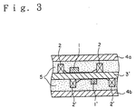
- a film of PET having a thickness of 80 ⁇ m which had IC chips having the maximum height of 240 ⁇ m and antenna coils disposed on both faces of the film was used as the substrate sheet.
- a coating layer of the sealing material composition obtained in Example 1 was formed in a manner such that the thickness was 260 ⁇ m after being cured.
- a transparent film of PET having a thickness of 80 ⁇ m was tightly placed as the cover sheet. Then, light was applied at the side of the cover sheet of the film of PET.
- the sealing material composition was cured and a laminate sheet having the cover sheet on one face was prepared.
Landscapes
- Engineering & Computer Science (AREA)
- Microelectronics & Electronic Packaging (AREA)
- Theoretical Computer Science (AREA)
- General Physics & Mathematics (AREA)
- Physics & Mathematics (AREA)
- Computer Hardware Design (AREA)
- Computer Networks & Wireless Communication (AREA)
- Chemical & Material Sciences (AREA)
- Organic Chemistry (AREA)
- Manufacturing & Machinery (AREA)
- Materials Engineering (AREA)
- Laminated Bodies (AREA)
- Macromonomer-Based Addition Polymer (AREA)
- Structures Or Materials For Encapsulating Or Coating Semiconductor Devices Or Solid State Devices (AREA)
- Sealing Material Composition (AREA)
- Adhesives Or Adhesive Processes (AREA)
- Paints Or Removers (AREA)
Abstract
Description
- 1 and 1':
- IC chips
- 2 and 2':
- Antennas
- 3 and 3':
- Substrate sheets
- 4, 4a and 4b:
- Cover sheets
- 5:
- A coating layer (a sealing material composition)
| Adhesive strength between layers (g/25 mm) | Separation between layers after bending test | Separation between layers after twisting test | |
| Example 1 | 2,500 | none | none |
| Example 2 | 2,200 | none | none |
| Example 3 | 2,800 | none | none |
| Example 4 | 3,500 | none | none |
| Comparative Example 1 | 800 | found | found |
Claims (2)
- A sealing material composition for cards which comprises (A) an acrylate compound polymerizable by an ionizing radiation and (B) 1 to 40 parts by weight of a polyfunctional isocyanate compound per 100 parts by weight of said acrylate compound and can be cured by irradiation of the ionizing radiation.
- A process for producing cards which comprises disposing a coating layer of a sealing material composition described in Claim 1 on a face of a substrate sheet on which an electronic chip and members related to the electronic chip are disposed, the electronic chip and the members being disposed at least on one of the faces of the substrate sheet, tightly placing a cover sheet on the coating layer and curing the sealing material composition by irradiating an ionizing radiation to the coating layer.
Applications Claiming Priority (2)
| Application Number | Priority Date | Filing Date | Title |
|---|---|---|---|
| JP24927499A JP2001072960A (en) | 1999-09-02 | 1999-09-02 | Card sealing material composition and card manufacturing method using the same |
| JP24927499 | 1999-09-02 |
Publications (2)
| Publication Number | Publication Date |
|---|---|
| EP1081201A1 true EP1081201A1 (en) | 2001-03-07 |
| EP1081201B1 EP1081201B1 (en) | 2005-02-09 |
Family
ID=17190535
Family Applications (1)
| Application Number | Title | Priority Date | Filing Date |
|---|---|---|---|
| EP00116279A Expired - Lifetime EP1081201B1 (en) | 1999-09-02 | 2000-08-09 | Sealing material composition for cards and process for producing cards using the composition |
Country Status (8)
| Country | Link |
|---|---|
| US (1) | US6592973B1 (en) |
| EP (1) | EP1081201B1 (en) |
| JP (1) | JP2001072960A (en) |
| KR (1) | KR100352925B1 (en) |
| CN (1) | CN1174055C (en) |
| DE (1) | DE60017997T2 (en) |
| SG (1) | SG86433A1 (en) |
| TW (1) | TW502058B (en) |
Cited By (2)
| Publication number | Priority date | Publication date | Assignee | Title |
|---|---|---|---|---|
| WO2006000849A1 (en) * | 2004-06-16 | 2006-01-05 | Axalto Sa | Secured identification document |
| CN109438657A (en) * | 2018-11-01 | 2019-03-08 | 无锡阿科力科技股份有限公司 | A kind of polyurethane acroleic acid oligomer and its preparation method and application |
Families Citing this family (9)
| Publication number | Priority date | Publication date | Assignee | Title |
|---|---|---|---|---|
| JP2002322464A (en) * | 2001-04-25 | 2002-11-08 | Ask Technica Corp | Sealing composition |
| US20050098904A1 (en) * | 2003-11-10 | 2005-05-12 | Pierre Liu | Transparent small memory card |
| WO2005089480A2 (en) | 2004-03-19 | 2005-09-29 | Stuart Arthur Bateman | Activation method |
| EP1828335B1 (en) | 2005-01-21 | 2010-03-10 | Commonwealth Scientific And Industrial Research Organisation | Activation method using modifying agent |
| KR100642889B1 (en) * | 2005-05-25 | 2006-11-03 | 엘에스전선 주식회사 | Adhesive film for semiconductor |
| KR100656364B1 (en) | 2005-11-15 | 2006-12-13 | 한국전자통신연구원 | Electronic Tag Encapsulant |
| FR2904321B1 (en) * | 2006-07-25 | 2008-09-05 | Rhodia Recherches Et Technologies Sas | POLYMERIZABLE AND / OR CROSS-LINKABLE COMPOSITION UNDER CATIONIC AND / OR RADICAL IRRADIATION |
| JP6115100B2 (en) * | 2012-11-23 | 2017-04-19 | デクセリアルズ株式会社 | Photocurable composition |
| EP4206248A4 (en) * | 2020-08-31 | 2025-04-02 | ThreeBond Co., Ltd. | CURABLE RESIN COMPOSITION, FUEL CELL, AND SEALING METHOD |
Citations (3)
| Publication number | Priority date | Publication date | Assignee | Title |
|---|---|---|---|---|
| EP0768353A1 (en) * | 1995-04-28 | 1997-04-16 | Nippon Kayaku Kabushiki Kaisha | Ultraviolet-curing adhesive composition |
| EP0835917A1 (en) * | 1996-04-25 | 1998-04-15 | Nippon Kayaku Kabushiki Kaisha | Ultraviolet-curing adhesive composition and article |
| EP0935288A2 (en) * | 1998-02-05 | 1999-08-11 | LINTEC Corporation | Sealed structure of semiconductor circuit and method for production thereof |
Family Cites Families (3)
| Publication number | Priority date | Publication date | Assignee | Title |
|---|---|---|---|---|
| US4424252A (en) * | 1982-11-12 | 1984-01-03 | Loctite Corporation | Conformal coating systems |
| JPH08319456A (en) * | 1995-04-28 | 1996-12-03 | E I Du Pont De Nemours & Co | Aqueous-system-treatable, flexible, optical-image-forming and durable coating material for printed circuit |
| US5866656A (en) * | 1995-06-07 | 1999-02-02 | National Starch And Chemical Investment Holding Corporation | Polyurethane hotmelt adhesives with reactive acrylic copolymers |
-
1999
- 1999-09-02 JP JP24927499A patent/JP2001072960A/en active Pending
-
2000
- 2000-08-09 DE DE60017997T patent/DE60017997T2/en not_active Expired - Fee Related
- 2000-08-09 EP EP00116279A patent/EP1081201B1/en not_active Expired - Lifetime
- 2000-08-17 SG SG200004560A patent/SG86433A1/en unknown
- 2000-08-21 US US09/641,951 patent/US6592973B1/en not_active Expired - Fee Related
- 2000-08-29 TW TW089117478A patent/TW502058B/en not_active IP Right Cessation
- 2000-09-01 CN CNB001264532A patent/CN1174055C/en not_active Expired - Fee Related
- 2000-09-02 KR KR1020000051817A patent/KR100352925B1/en not_active Expired - Fee Related
Patent Citations (3)
| Publication number | Priority date | Publication date | Assignee | Title |
|---|---|---|---|---|
| EP0768353A1 (en) * | 1995-04-28 | 1997-04-16 | Nippon Kayaku Kabushiki Kaisha | Ultraviolet-curing adhesive composition |
| EP0835917A1 (en) * | 1996-04-25 | 1998-04-15 | Nippon Kayaku Kabushiki Kaisha | Ultraviolet-curing adhesive composition and article |
| EP0935288A2 (en) * | 1998-02-05 | 1999-08-11 | LINTEC Corporation | Sealed structure of semiconductor circuit and method for production thereof |
Cited By (3)
| Publication number | Priority date | Publication date | Assignee | Title |
|---|---|---|---|---|
| WO2006000849A1 (en) * | 2004-06-16 | 2006-01-05 | Axalto Sa | Secured identification document |
| US8973834B2 (en) | 2004-06-16 | 2015-03-10 | Gemalto Sa | Secured identification document |
| CN109438657A (en) * | 2018-11-01 | 2019-03-08 | 无锡阿科力科技股份有限公司 | A kind of polyurethane acroleic acid oligomer and its preparation method and application |
Also Published As
| Publication number | Publication date |
|---|---|
| TW502058B (en) | 2002-09-11 |
| JP2001072960A (en) | 2001-03-21 |
| SG86433A1 (en) | 2002-02-19 |
| CN1174055C (en) | 2004-11-03 |
| KR20010050318A (en) | 2001-06-15 |
| US6592973B1 (en) | 2003-07-15 |
| EP1081201B1 (en) | 2005-02-09 |
| CN1287139A (en) | 2001-03-14 |
| KR100352925B1 (en) | 2002-09-16 |
| DE60017997D1 (en) | 2005-03-17 |
| DE60017997T2 (en) | 2005-07-07 |
Similar Documents
| Publication | Publication Date | Title |
|---|---|---|
| EP1081201B1 (en) | Sealing material composition for cards and process for producing cards using the composition | |
| EP0835917B1 (en) | Ultraviolet-curing adhesive composition and article | |
| EP1120824A2 (en) | Process for producing an ic chip having a protective layer | |
| US6017603A (en) | Ultraviolet-curing adhesive composition and article | |
| KR101161941B1 (en) | Wafer-processing film | |
| KR102016578B1 (en) | Base film and pressure-sensitive adhesive sheet provided therewith | |
| EP0768353A1 (en) | Ultraviolet-curing adhesive composition | |
| US20120319305A1 (en) | Process for producing a sheet of a circuit substrate | |
| JPH0417148B2 (en) | ||
| JP5010800B2 (en) | Manufacturing method of semiconductor device and adhesive tape for dicing | |
| JPS63110224A (en) | Flexible overlay film | |
| EP0503782A1 (en) | Integrated circuit card | |
| JP2009295874A (en) | Flexible printed circuit board and method of manufacturing the same | |
| JP2874482B2 (en) | Temporary surface protection method and resin composition used therefor | |
| JP4422547B2 (en) | Dry film and processed product using the same | |
| JP4416897B2 (en) | IC card manufacturing process material and IC card manufacturing method | |
| JP2024129280A (en) | Electrically conductive adhesive composition and method of using the electrically conductive adhesive composition | |
| JP2008010714A (en) | Manufacturing method of electromagnetic wave shielding material | |
| JPH03297638A (en) | Production of copper foil coated with radiation hardening type coating | |
| JP2000242757A (en) | Manufacturing method of non-contact IC card | |
| CN104109489B (en) | Cover layer and use its copper clad laminate | |
| JP2006323335A (en) | Sheet for circuit board and circuit board sheet for display | |
| JPH1046119A (en) | Pressure-sensitive adhesive film used in production of ivh-containing multilayer wiring board | |
| JP2004017320A (en) | IC card and manufacturing method thereof | |
| WO2025115683A1 (en) | Heat-resistant adhesive film |
Legal Events
| Date | Code | Title | Description |
|---|---|---|---|
| PUAI | Public reference made under article 153(3) epc to a published international application that has entered the european phase |
Free format text: ORIGINAL CODE: 0009012 |
|
| AK | Designated contracting states |
Kind code of ref document: A1 Designated state(s): DE FR GB IT |
|
| AX | Request for extension of the european patent |
Free format text: AL;LT;LV;MK;RO;SI |
|
| 17P | Request for examination filed |
Effective date: 20010813 |
|
| AKX | Designation fees paid |
Free format text: DE FR GB IT |
|
| GRAP | Despatch of communication of intention to grant a patent |
Free format text: ORIGINAL CODE: EPIDOSNIGR1 |
|
| GRAS | Grant fee paid |
Free format text: ORIGINAL CODE: EPIDOSNIGR3 |
|
| GRAA | (expected) grant |
Free format text: ORIGINAL CODE: 0009210 |
|
| AK | Designated contracting states |
Kind code of ref document: B1 Designated state(s): DE FR GB IT |
|
| REG | Reference to a national code |
Ref country code: GB Ref legal event code: FG4D |
|
| REF | Corresponds to: |
Ref document number: 60017997 Country of ref document: DE Date of ref document: 20050317 Kind code of ref document: P |
|
| PLBE | No opposition filed within time limit |
Free format text: ORIGINAL CODE: 0009261 |
|
| STAA | Information on the status of an ep patent application or granted ep patent |
Free format text: STATUS: NO OPPOSITION FILED WITHIN TIME LIMIT |
|
| ET | Fr: translation filed | ||
| 26N | No opposition filed |
Effective date: 20051110 |
|
| PGFP | Annual fee paid to national office [announced via postgrant information from national office to epo] |
Ref country code: DE Payment date: 20060803 Year of fee payment: 7 |
|
| PGFP | Annual fee paid to national office [announced via postgrant information from national office to epo] |
Ref country code: FR Payment date: 20060808 Year of fee payment: 7 |
|
| PGFP | Annual fee paid to national office [announced via postgrant information from national office to epo] |
Ref country code: GB Payment date: 20060809 Year of fee payment: 7 |
|
| PGFP | Annual fee paid to national office [announced via postgrant information from national office to epo] |
Ref country code: IT Payment date: 20060831 Year of fee payment: 7 |
|
| GBPC | Gb: european patent ceased through non-payment of renewal fee |
Effective date: 20070809 |
|
| REG | Reference to a national code |
Ref country code: FR Ref legal event code: ST Effective date: 20080430 |
|
| PG25 | Lapsed in a contracting state [announced via postgrant information from national office to epo] |
Ref country code: DE Free format text: LAPSE BECAUSE OF NON-PAYMENT OF DUE FEES Effective date: 20080301 |
|
| PG25 | Lapsed in a contracting state [announced via postgrant information from national office to epo] |
Ref country code: FR Free format text: LAPSE BECAUSE OF NON-PAYMENT OF DUE FEES Effective date: 20070831 |
|
| PG25 | Lapsed in a contracting state [announced via postgrant information from national office to epo] |
Ref country code: GB Free format text: LAPSE BECAUSE OF NON-PAYMENT OF DUE FEES Effective date: 20070809 |
|
| PG25 | Lapsed in a contracting state [announced via postgrant information from national office to epo] |
Ref country code: IT Free format text: LAPSE BECAUSE OF NON-PAYMENT OF DUE FEES Effective date: 20070809 |