EP1079620A2 - Programmable digital signal processor for demodulating digital television signals - Google Patents
Programmable digital signal processor for demodulating digital television signals Download PDFInfo
- Publication number
- EP1079620A2 EP1079620A2 EP00114882A EP00114882A EP1079620A2 EP 1079620 A2 EP1079620 A2 EP 1079620A2 EP 00114882 A EP00114882 A EP 00114882A EP 00114882 A EP00114882 A EP 00114882A EP 1079620 A2 EP1079620 A2 EP 1079620A2
- Authority
- EP
- European Patent Office
- Prior art keywords
- block
- phase
- circuit
- samples
- digital signal
- Prior art date
- Legal status (The legal status is an assumption and is not a legal conclusion. Google has not performed a legal analysis and makes no representation as to the accuracy of the status listed.)
- Withdrawn
Links
Images


Classifications
-
- H—ELECTRICITY
- H04—ELECTRIC COMMUNICATION TECHNIQUE
- H04L—TRANSMISSION OF DIGITAL INFORMATION, e.g. TELEGRAPHIC COMMUNICATION
- H04L7/00—Arrangements for synchronising receiver with transmitter
- H04L7/0016—Arrangements for synchronising receiver with transmitter correction of synchronization errors
- H04L7/002—Arrangements for synchronising receiver with transmitter correction of synchronization errors correction by interpolation
- H04L7/0029—Arrangements for synchronising receiver with transmitter correction of synchronization errors correction by interpolation interpolation of received data signal
-
- H—ELECTRICITY
- H04—ELECTRIC COMMUNICATION TECHNIQUE
- H04L—TRANSMISSION OF DIGITAL INFORMATION, e.g. TELEGRAPHIC COMMUNICATION
- H04L27/00—Modulated-carrier systems
- H04L27/32—Carrier systems characterised by combinations of two or more of the types covered by groups H04L27/02, H04L27/10, H04L27/18 or H04L27/26
- H04L27/34—Amplitude- and phase-modulated carrier systems, e.g. quadrature-amplitude modulated carrier systems
- H04L27/38—Demodulator circuits; Receiver circuits
-
- H—ELECTRICITY
- H04—ELECTRIC COMMUNICATION TECHNIQUE
- H04N—PICTORIAL COMMUNICATION, e.g. TELEVISION
- H04N21/00—Selective content distribution, e.g. interactive television or video on demand [VOD]
- H04N21/40—Client devices specifically adapted for the reception of or interaction with content, e.g. set-top-box [STB]; Operations thereof
- H04N21/41—Structure of client; Structure of client peripherals
- H04N21/426—Internal components of the client ; Characteristics thereof
- H04N21/42607—Internal components of the client ; Characteristics thereof for processing the incoming bitstream
-
- H—ELECTRICITY
- H04—ELECTRIC COMMUNICATION TECHNIQUE
- H04N—PICTORIAL COMMUNICATION, e.g. TELEVISION
- H04N21/00—Selective content distribution, e.g. interactive television or video on demand [VOD]
- H04N21/40—Client devices specifically adapted for the reception of or interaction with content, e.g. set-top-box [STB]; Operations thereof
- H04N21/43—Processing of content or additional data, e.g. demultiplexing additional data from a digital video stream; Elementary client operations, e.g. monitoring of home network or synchronising decoder's clock; Client middleware
- H04N21/438—Interfacing the downstream path of the transmission network originating from a server, e.g. retrieving encoded video stream packets from an IP network
- H04N21/4382—Demodulation or channel decoding, e.g. QPSK demodulation
-
- H—ELECTRICITY
- H04—ELECTRIC COMMUNICATION TECHNIQUE
- H04L—TRANSMISSION OF DIGITAL INFORMATION, e.g. TELEGRAPHIC COMMUNICATION
- H04L27/00—Modulated-carrier systems
- H04L27/0014—Carrier regulation
- H04L2027/0024—Carrier regulation at the receiver end
- H04L2027/0026—Correction of carrier offset
- H04L2027/003—Correction of carrier offset at baseband only
-
- H—ELECTRICITY
- H04—ELECTRIC COMMUNICATION TECHNIQUE
- H04L—TRANSMISSION OF DIGITAL INFORMATION, e.g. TELEGRAPHIC COMMUNICATION
- H04L27/00—Modulated-carrier systems
- H04L27/0014—Carrier regulation
- H04L2027/0024—Carrier regulation at the receiver end
- H04L2027/0026—Correction of carrier offset
- H04L2027/0038—Correction of carrier offset using an equaliser
- H04L2027/0042—Correction of carrier offset using an equaliser the equaliser providing the offset correction per se
-
- H—ELECTRICITY
- H04—ELECTRIC COMMUNICATION TECHNIQUE
- H04L—TRANSMISSION OF DIGITAL INFORMATION, e.g. TELEGRAPHIC COMMUNICATION
- H04L27/00—Modulated-carrier systems
- H04L27/0014—Carrier regulation
- H04L2027/0044—Control loops for carrier regulation
- H04L2027/0053—Closed loops
- H04L2027/0057—Closed loops quadrature phase
-
- H—ELECTRICITY
- H04—ELECTRIC COMMUNICATION TECHNIQUE
- H04N—PICTORIAL COMMUNICATION, e.g. TELEVISION
- H04N21/00—Selective content distribution, e.g. interactive television or video on demand [VOD]
- H04N21/40—Client devices specifically adapted for the reception of or interaction with content, e.g. set-top-box [STB]; Operations thereof
- H04N21/41—Structure of client; Structure of client peripherals
- H04N21/426—Internal components of the client ; Characteristics thereof
-
- H—ELECTRICITY
- H04—ELECTRIC COMMUNICATION TECHNIQUE
- H04N—PICTORIAL COMMUNICATION, e.g. TELEVISION
- H04N5/00—Details of television systems
- H04N5/44—Receiver circuitry for the reception of television signals according to analogue transmission standards
- H04N5/455—Demodulation-circuits
Definitions
- This invention relates generally to demodulators for digital television receivers, and more particularly to phase-lock loop units in demodulator front-ends.
- MPEG-2 is the common standard for video coding at the source of television signals. Because of the similarity in video coding in the three transmission media, it is possible to share signal processing functional blocks in receivers for the three media. This is the so-called multi-mode digital television receiver.
- the conventional approach for implementing demodulators dictates a hardware solution. This is due to the high symbol rates, i.e., 10.76MHz for 8VSB, 5.38MHz for 256QAM, and up to 45MHz for QPSK. Symbols can be, for example, six or eight bits. Hardware offers computational speed not attainable by software. However, specialized hardware is very difficult to change for future upgrades, the size of the chip is large, and the cost is relatively high when compared with implementation that use software and common digital signal processors.
- a phase-lock loop circuit in a demodulator includes a timing recovery block and a carrier recovery block.
- the demodulator for demodulates a digital signal including symbols. The symbols are sampled at a time interval equal to or a fraction of the symbol rate.
- the phase-lock loop includes an integrator processing a block of N samples to produce an average of the N samples, and means for supplying the average to the timing recovery block and the carrier recovery block every NT period, where T is a sample interval.
- the phase-lock loop is under software control and can operate in any one of three block-based modes as determined by a frequency offset.
- Figure 1 shows a multi-mode demodulator front-end 100 for a multi-mode digital television receiver.
- the demodulator front-end 100 is implemented with general purpose programmable digital signal processors, and reconfigurable logic.
- the demodulator front-end 100 includes a timing recovery (TR) block 110, a carrier recovery (CR) block 120, and an equalizer (EQ) 130.
- the front-end 100 receives a television signal as input 101 via an A/D unit, e.g., a tuner.
- a master clock 102 provides timing signals to the demodulator.
- the front-end can produce I and Q channels 103 as output to a forward error correction (FEC) unit.
- FEC forward error correction
- the TR, CR and EQ are all implemented in complex mode as both I and Q channels are used.
- the TR, CR and EQ are all implemented in complex mode as both I and Q channels are used.
- VSB one has the choice of processing only the I channel, or processing both the I and Q channels. Under ideal reception condition, only the I channel contains information.
- the Q channel may provide improvements in non-ideal reception conditions.
- the timing recovery block 110 uses an unsynchronized scheme as described by Bao et al. in "A New Timing Recovery Method For DTV Receivers," IEEE Trans. On Consumer Electronics, Vol. 44, No.4, pp. 1243-1249, 1998. Because of the high data rate, the input of the TR (interpolator) is implemented in configurable logic. The details of the logic design and implementation is described by Lu et al. in “Data receiver having variable rate symbol timing recovery with non-synchronized sampling,” U.S. Patent Application Sn. 08/997,772.
- the PLL can be an element shared by both recovery circuits.
- the PLL for both timing and carrier blocks is implemented with software programmable digital signal processors (DSP) which processes a block of N samples at the time, instead of processing individual symbols. The processing produces an average of the block of N samples.
- DSP software programmable digital signal processors
- Figure 2 shows the basic elements of a phase-lock loop circuit 200.
- the circuit includes a phase detector 210, a loop filter 220, and a numerically controlled oscillator (NCO) 230.
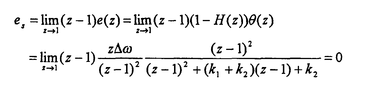
- Figure 3 shows the PLL 200 as an approximated linear model while the PLL is in a steady state.
- I(z) and O(z) are Z -transforms of the input and output of the loop filter respectively, and k1 and k2 are the loop gain control parameters.
- the mean square error (MSE) of the phase error is equal to the variance of phase error which is in turn is a function of the loop gains k 1 and k 2 .
- output V k of the loop filter 220 is approximately equal to the frequency offset ⁇ ⁇ statistically as: ⁇ k +1 - ⁇ k which is small in magnitude.
- FIG. 6 shows a PLL circuit 600 for the CR block 120 of Figure 1.
- the PLL 600 includes a phase detector 610, a loop filter 620, and a NCO 630.
- the PLL 600 also includes an integrator 640 between the phase detector and the loop filter.
- the phase detector 610 extracts a phase error from the output Xn of the equalizer 130.
- the loop filter 620 is a low-pass filter with two gain control parameters k 1 and k 2 . It is possible to tune the PLL 600 for best performance based on a particular different mode by adjusting k 1 and k 2 .
- the integrator 640 takes an average of a block of N samples.
- the block size N can vary during different states, such as the acquisition state and the tracking state as described below.
- the average is supplied to the loop filter 630 every NT periods, where T is the sample time interval.
- the sample rate, or 1/T is twice of the input symbol rate; for carrier recover circuit, 1/T is the same as the symbol rate.
- both elements can be implemented using software executing in a DSP.
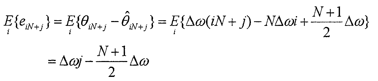
- the loop filter output Vk for block-based updating is N times larger than it would be for sample rate-based updating. This is equivalent to a N ⁇ ⁇ frequency offset in sample rate-based updating scheme. If k 1 and k 2 are the same for both schemes, convergence time is about N times as in conventional sample rate-based updating.
- the mean of the phase error is related to j which causes phase spread.
- FIG. 8 An alternative structure 800 is shown in Figure 8.
- sample rate-based updating is used in the NCO 630.
- N 1 Sample rate-Based Updating Frequency offset ⁇ f (kHz) 10 50 100 150 Convergence time Tc (ksym) 3 8 10 80 Convergence time Tc (msec) 0.56 1.49 1.86 14.87 MSE ⁇ 2 4.07E-06 6.54E-06 9.44E-06 1.11E-05
- loop filter operates about ten times slower this performance is almost the same as sample rate-based updating. Since loop filter is operated 10 times slower than sample rate-based updating, the operating speed is reduced by about a factor often.
- the method updates timing and carrier recovery blocks, as well as other blocks, on a periodic basis, that is, a block of symbols, and not for every symbol as in the prior art.
- this method offers a completely programmable solution for the design of a digital television receiver demodulator front-end.
- the block-based approach reduces processing speed by using adaptive block processing. Compared to sample rate-based updating that uses logic circuits, the block based updating has good performance with high flexibility, and thus is particularly suitable for multi-mode applications.
- the first structure which updates in both the phase detector and the loop filter, is the simplest to implement.
- the first alternative structure that updates only in the loop filter is preferred when the men square error is a concern.
- the second alternative offers the most reduction of implementation complexity, at a higher mean square error.
- the block factor N should be relatively small to allow rapid lock on the carrier during initial signal acquisition, for example, in the range of two to four. Notice. a blocks size of one corresponds to sample rate-based updating. After a lock on carrier has been achieved, a larger block size, e.g., ten, can be used during tracking.
- the switching between acquisition mode and tracking mode is determined by the mean square error and the constellation diagram that graphical representations in two dimensions the carrier amplitude and phase at each sampling time.
- the invention can also used in an automatic gain control (AGC) loop that uses a phase-lock loop.
- AGC automatic gain control
- the processing speed requirements of AGC are much smaller than the symbol rate, thus making a DSP implementation desirable.
Landscapes
- Engineering & Computer Science (AREA)
- Signal Processing (AREA)
- Multimedia (AREA)
- Computer Networks & Wireless Communication (AREA)
- Stabilization Of Oscillater, Synchronisation, Frequency Synthesizers (AREA)
- Digital Transmission Methods That Use Modulated Carrier Waves (AREA)
- Synchronizing For Television (AREA)
Abstract
Description
| N=1 Sample rate-Based Updating | ||||
| Frequency offset Δf (kHz) | 10 | 50 | 100 | 150 |
| Convergence time Tc (ksym) | 3 | 8 | 10 | 80 |
| Convergence time Tc (msec) | 0.56 | 1.49 | 1.86 | 14.87 |
| MSE σ^ 2 | 4.07E-06 | 6.54E-06 | 9.44E-06 | 1.11E-05 |
| N=10 Block-Based Updating in Loop Filter | ||||
| Frequency offset Δf (kHz) | 10 | 50 | 100 | 150 |
| Convergence time Tc (ksym) | 3 | 8 | 16 | 84 |
| Convergence time Tc (msec) | 0.56 | 1.49 | 2.97 | 15.61 |
| MSE σ^2 | 1.49E-06 | 5.86E-06 | 6.26E-06 | 4.56E-06 |
| N=10 Block-Based Updating in Phase Detector | ||||
| Frequency offset Δf (kHz) | 10 | 50 | 100 | 150 |
| Convergence time Tc (ksym) | 13 | 25 | 32 | 84 |
| Convergence time Tc (msec) | 2.42 | 4.65 | 5.95 | 15.61 |
| MSE σ^ 2 | 2.08E-05 | 4.67E-05 | 3.05E-05 | 4.18E-05 |
Claims (10)
- A phase-lock loop circuit in a demodulator including a timing recovery block and a carrier recovery block, the demodulator for demodulating a digital signal including symbols, comprising:an integrator processing a block of N samples of the digital signal to produce an average of the block of N samples;means for supplying the average to the timing recovery block and the carrier recovery block every NT period, where T is a sample time interval.
- The circuit of claim 1 wherein the integrator is a software programmable digital signal processor.
- The circuit of claim 1 wherein the integrator couples a phase detector and a loop filter of the phase-lock loop circuit.
- The circuit of claim 1 wherein N is less than twenty.
- The circuit of claim 1 wherein the phase-lock loop includes a phase detector processing the block of N samples.
- The circuit of claim 1 wherein the phase-lock includes a loop filter and a numerically controlled oscillator processing the block of N samples.
- The circuit of claim 6 wherein the loop filter is updated over N samples, N> 1 and the phase detector and numerically controlled oscillator are updated at a sample rate.
- The circuit of claim 1 wherein the phase-lock loop uses a block-based phase detector.
- The circuit of claim 1 wherein the demodulator is under software control to operate in sample rate mode or block mode dependent on a frequency offset and carrier and timing acquisition condition.
- The circuit of claim 1 where the samples are symbols when a sample rate is identical to a symbol rate.
Applications Claiming Priority (2)
| Application Number | Priority Date | Filing Date | Title |
|---|---|---|---|
| US09/366,005 US6577685B1 (en) | 1999-08-02 | 1999-08-02 | Programmable digital signal processor for demodulating digital television signals |
| US366005 | 2002-03-20 |
Publications (2)
| Publication Number | Publication Date |
|---|---|
| EP1079620A2 true EP1079620A2 (en) | 2001-02-28 |
| EP1079620A3 EP1079620A3 (en) | 2004-03-03 |
Family
ID=23441303
Family Applications (1)
| Application Number | Title | Priority Date | Filing Date |
|---|---|---|---|
| EP00114882A Withdrawn EP1079620A3 (en) | 1999-08-02 | 2000-07-12 | Programmable digital signal processor for demodulating digital television signals |
Country Status (3)
| Country | Link |
|---|---|
| US (1) | US6577685B1 (en) |
| EP (1) | EP1079620A3 (en) |
| JP (1) | JP2001077871A (en) |
Families Citing this family (20)
| Publication number | Priority date | Publication date | Assignee | Title |
|---|---|---|---|---|
| AU9213398A (en) * | 1997-12-12 | 1999-07-05 | Thomson Consumer Electronics, Inc | Tdma wireless telephone system with independently tracked demodulation parameters |
| CN1989751B (en) * | 2004-07-15 | 2011-07-13 | 汤姆森特许公司 | System and method for improved carrier recovery |
| KR100577703B1 (en) * | 2004-08-27 | 2006-05-10 | 삼성전자주식회사 | Carrier Restoration Apparatus for UBS Receiver and Its Restoration Method |
| DE102005023909B3 (en) | 2005-05-24 | 2006-10-12 | Infineon Technologies Ag | Digital phase locked loop for mobile communication terminal, has correction circuit generating correction words derived from frequency correction words inputted to input of integrator and words derived from frequency word of input terminal |
| WO2007091779A1 (en) | 2006-02-10 | 2007-08-16 | Lg Electronics Inc. | Digital broadcasting receiver and method of processing data |
| WO2007126196A1 (en) | 2006-04-29 | 2007-11-08 | Lg Electronics Inc. | Digital broadcasting system and method of processing data |
| WO2007136166A1 (en) | 2006-05-23 | 2007-11-29 | Lg Electronics Inc. | Digital broadcasting system and method of processing data |
| US7873104B2 (en) * | 2006-10-12 | 2011-01-18 | Lg Electronics Inc. | Digital television transmitting system and receiving system and method of processing broadcasting data |
| US8385397B2 (en) * | 2007-01-19 | 2013-02-26 | Techwell Llc | Method for determining the step size for an LMS adaptive equalizer for 8VSB |
| US7616685B2 (en) * | 2007-01-19 | 2009-11-10 | Techwell, Inc. | Method for channel tracking in an LMS adaptive equalizer for 8VSB |
| KR101285887B1 (en) | 2007-03-26 | 2013-07-11 | 엘지전자 주식회사 | Digital broadcasting system and method of processing data in digital broadcasting system |
| KR101253185B1 (en) | 2007-03-26 | 2013-04-10 | 엘지전자 주식회사 | Digital broadcasting system and data processing method |
| KR101285888B1 (en) | 2007-03-30 | 2013-07-11 | 엘지전자 주식회사 | Digital broadcasting system and method of processing data in digital broadcasting system |
| US8433973B2 (en) * | 2007-07-04 | 2013-04-30 | Lg Electronics Inc. | Digital broadcasting system and method of processing data |
| WO2009005326A2 (en) | 2007-07-04 | 2009-01-08 | Lg Electronics Inc. | Digital broadcasting system and method of processing data |
| KR20090012180A (en) | 2007-07-28 | 2009-02-02 | 엘지전자 주식회사 | Digital broadcasting system and data processing method |
| MX2010002146A (en) | 2007-08-24 | 2010-04-07 | Lg Electronics Inc | Digital broadcasting system and method of processing data in digital broadcasting system. |
| US8731074B2 (en) * | 2008-09-17 | 2014-05-20 | Harris Corporation | Communications device using measured frequency offset over time to adjust phase and frequency tracking |
| US8565324B2 (en) * | 2008-09-17 | 2013-10-22 | Harris Corporation | Communications device using measured signal-to-noise ratio to adjust phase and frequency tracking |
| CN105745931B (en) * | 2013-11-24 | 2019-06-25 | Lg电子株式会社 | Method and apparatus for encoding and decoding video signals using adaptive sampling |
Family Cites Families (15)
| Publication number | Priority date | Publication date | Assignee | Title |
|---|---|---|---|---|
| JP2932289B2 (en) * | 1989-11-24 | 1999-08-09 | 株式会社富士通ゼネラル | 4 phase demodulation circuit |
| US5249204A (en) * | 1991-08-12 | 1993-09-28 | Motorola, Inc. | Circuit and method for phase error correction in a digital receiver |
| JPH05145414A (en) * | 1991-11-21 | 1993-06-11 | Matsushita Electric Ind Co Ltd | Automatic frequency controller |
| JPH06197140A (en) * | 1992-10-28 | 1994-07-15 | Hitachi Ltd | Digital demodulating circuit |
| US5373255A (en) * | 1993-07-28 | 1994-12-13 | Motorola, Inc. | Low-power, jitter-compensated phase locked loop and method therefor |
| JP3085511B2 (en) * | 1994-11-24 | 2000-09-11 | 株式会社アドバンテスト | Reference frequency generator |
| US5739874A (en) * | 1995-06-06 | 1998-04-14 | Thomson Consumer Electronics, Inc. | Tuning system for a digital satellite receiver with fine tuning provisions |
| WO1997003510A1 (en) * | 1995-07-07 | 1997-01-30 | Northern Telecom Limited | Carrier recovery for digitally phase modulated signals, using a known sequence |
| KR0170690B1 (en) * | 1995-09-23 | 1999-03-20 | 김광호 | Carrier and Symbol Timing Restoration Completion Detection Circuit and Its Method and Its High Resolution Television |
| EP0774850B1 (en) * | 1995-11-16 | 2004-10-27 | Ntt Mobile Communications Network Inc. | Digital signal detecting method and detector |
| JPH09168039A (en) * | 1995-12-15 | 1997-06-24 | Toshiba Corp | Carrier recovery circuit |
| JP3592489B2 (en) * | 1996-07-22 | 2004-11-24 | 日本電信電話株式会社 | Clock timing recovery method and circuit |
| US5898334A (en) * | 1997-05-12 | 1999-04-27 | Elantec Semiconductor, Inc. | Reduced output capacitance circuit for driving a grounded load in response to a stepped input |
| JP3271180B2 (en) * | 1997-06-27 | 2002-04-02 | 三洋電機株式会社 | Data demodulator |
| US6411661B1 (en) * | 1999-05-07 | 2002-06-25 | The Aerospace Corporation | Digital timing recovery loop for GMSK demodulators |
-
1999
- 1999-08-02 US US09/366,005 patent/US6577685B1/en not_active Expired - Fee Related
-
2000
- 2000-07-06 JP JP2000205022A patent/JP2001077871A/en active Pending
- 2000-07-12 EP EP00114882A patent/EP1079620A3/en not_active Withdrawn
Also Published As
| Publication number | Publication date |
|---|---|
| EP1079620A3 (en) | 2004-03-03 |
| JP2001077871A (en) | 2001-03-23 |
| US6577685B1 (en) | 2003-06-10 |
Similar Documents
| Publication | Publication Date | Title |
|---|---|---|
| EP1079620A2 (en) | Programmable digital signal processor for demodulating digital television signals | |
| US6707861B1 (en) | Demodulator for an HDTV receiver | |
| EP1364479B1 (en) | Satellite receiver and corresponding method | |
| US6298100B1 (en) | Phase error estimation method for a demodulator in an HDTV receiver | |
| CN102209216B (en) | Multi-standard digital demodulator for TV signals broadcast over cable, satellite and terrestrial networks | |
| JP3423547B2 (en) | Phase error correction method and phase tracking loop circuit | |
| EP0801866B1 (en) | Phase detector in a carrier recovery network for a vestigial sideband signal | |
| US6313885B1 (en) | DTV receiver with baseband equalization filters for QAM signal and for VSB signal which employ common elements | |
| US5706057A (en) | Phase detector in a carrier recovery network for a vestigial sideband signal | |
| US7027528B2 (en) | Timing recovery using the pilot signal in high definition TV | |
| US7016446B1 (en) | Channel decoder for a digital broadcast receiver | |
| KR100812554B1 (en) | Timing recovery system for a digital signal processor | |
| WO2005067250A1 (en) | Method and apparatus for compensating i/q imbalance in receivers | |
| JP2971028B2 (en) | Phase detection method and phase tracking loop circuit for digital vestigial sideband modulation communication device | |
| US6765623B1 (en) | Method and apparatus for correcting phase imbalance in received in-phase and quadrature signals | |
| US5812927A (en) | System and method for correction of I/Q angular error in a satellite receiver | |
| JP2002190989A (en) | Digital VSB detector with bandpass phase tracker using radar filter for use in HDTV receiver | |
| US6665355B1 (en) | Method and apparatus for pilot-aided carrier acquisition of vestigial sideband signal | |
| US5995563A (en) | System and method for fast channel switching in a satellite receiver | |
| CN100589537C (en) | Channel acquisition method and device for television receiver | |
| KR100720983B1 (en) | Method and apparatus for performing carrier acquisition of television signal having pilot tone | |
| US6421403B1 (en) | Baseband equalization of quadrature-phase as well as in-phase synchrodyne results in digital radio receivers | |
| KR100309097B1 (en) | Method and apparatus of fine tuning for television receiver and method and apparatus of matching vsb signal | |
| KR100745382B1 (en) | Timing Restoration Network for Digital Signal Processors | |
| JPH09247571A (en) | Signal receiver |
Legal Events
| Date | Code | Title | Description |
|---|---|---|---|
| PUAI | Public reference made under article 153(3) epc to a published international application that has entered the european phase |
Free format text: ORIGINAL CODE: 0009012 |
|
| AK | Designated contracting states |
Kind code of ref document: A2 Designated state(s): AT BE CH CY DE DK ES FI FR GB GR IE IT LI LU MC NL PT SE |
|
| AX | Request for extension of the european patent |
Free format text: AL;LT;LV;MK;RO;SI |
|
| PUAL | Search report despatched |
Free format text: ORIGINAL CODE: 0009013 |
|
| AK | Designated contracting states |
Kind code of ref document: A3 Designated state(s): AT BE CH CY DE DK ES FI FR GB GR IE IT LI LU MC NL PT SE |
|
| AX | Request for extension of the european patent |
Extension state: AL LT LV MK RO SI |
|
| AKX | Designation fees paid | ||
| REG | Reference to a national code |
Ref country code: DE Ref legal event code: 8566 |
|
| STAA | Information on the status of an ep patent application or granted ep patent |
Free format text: STATUS: THE APPLICATION IS DEEMED TO BE WITHDRAWN |
|
| 18D | Application deemed to be withdrawn |
Effective date: 20040904 |