EP1079526A1 - Logic gate - Google Patents
Logic gate Download PDFInfo
- Publication number
- EP1079526A1 EP1079526A1 EP00303979A EP00303979A EP1079526A1 EP 1079526 A1 EP1079526 A1 EP 1079526A1 EP 00303979 A EP00303979 A EP 00303979A EP 00303979 A EP00303979 A EP 00303979A EP 1079526 A1 EP1079526 A1 EP 1079526A1
- Authority
- EP
- European Patent Office
- Prior art keywords
- node
- pull
- transistor
- input
- output
- Prior art date
- Legal status (The legal status is an assumption and is not a legal conclusion. Google has not performed a legal analysis and makes no representation as to the accuracy of the status listed.)
- Withdrawn
Links
Images



Classifications
-
- H—ELECTRICITY
- H03—ELECTRONIC CIRCUITRY
- H03K—PULSE TECHNIQUE
- H03K19/00—Logic circuits, i.e. having at least two inputs acting on one output; Inverting circuits
- H03K19/01—Modifications for accelerating switching
- H03K19/017—Modifications for accelerating switching in field-effect transistor circuits
- H03K19/01707—Modifications for accelerating switching in field-effect transistor circuits in asynchronous circuits
-
- H—ELECTRICITY
- H03—ELECTRONIC CIRCUITRY
- H03K—PULSE TECHNIQUE
- H03K19/00—Logic circuits, i.e. having at least two inputs acting on one output; Inverting circuits
- H03K19/02—Logic circuits, i.e. having at least two inputs acting on one output; Inverting circuits using specified components
- H03K19/08—Logic circuits, i.e. having at least two inputs acting on one output; Inverting circuits using specified components using semiconductor devices
- H03K19/094—Logic circuits, i.e. having at least two inputs acting on one output; Inverting circuits using specified components using semiconductor devices using field-effect transistors
- H03K19/0944—Logic circuits, i.e. having at least two inputs acting on one output; Inverting circuits using specified components using semiconductor devices using field-effect transistors using MOSFET or insulated gate field-effect transistors, i.e. IGFET
- H03K19/0948—Logic circuits, i.e. having at least two inputs acting on one output; Inverting circuits using specified components using semiconductor devices using field-effect transistors using MOSFET or insulated gate field-effect transistors, i.e. IGFET using CMOS or complementary insulated gate field-effect transistors
Definitions
- the present invention relates to a logic gate and more specifically to an FET logic gate of the so-called ratio logic family.
- ratio logic There is known in the art a number of different logic families, one of which is termed ratio logic.
- ratio logic a pull-up device is connected between a high supply potential and a circuit node and a number of pull-down devices are connected between the circuit node and a negative supply potential.
- the pull-up device is permanently enabled and thus the circuit node is at a high potential provided the pull-down device are all inoperative. When one or more pull-down devices operates then the circuit node is at a relatively low level.
- the pull-up device is a PMOS transistor and the pull-down devices are NMOS transistors.
- the PMOS transistor must be of weaker conductivity than one NMOS, otherwise the output node will not be pulled down sufficiently to indicate a change in logic state.
- the requirement for a weak PMOS extends the pull-up time of the circuit node. This is because allowance must be made during design for the p transistors of a circuit to be at the strong end of their tolerance and the n transistors to be at the weak ends of their tolerance. Then, when the opposite process conditions appear, namely the p transistors being weaker than expected and the n transistors being stronger than expected the pull-up time may be excessive; it is this worst case rise time which is specified for the circuit.
- a logic gate comprising a current mirror circuit having a supply node, a first node and a second node wherein application of a first current at the first node causes a second current at the second node, plural input pull-down transistors connected between a reference node and one of said first and second nodes, and an output pull-down transistor connected between the other of said first and second nodes, and the reference terminal wherein the supply node has a connection to a supply terminal, the plural input pull-down transistors have respective control terminals connected to a corresponding plurality of input terminals and the output pull-down transistor has circuitry connected to its control node for biasing it on wherein said input pull-down transistors are mutually substantially identical and wherein said output pull-down transistor is smaller than each said input pull-down transistor.
- said plural input transistors are connected to said first node.
- the current mirror circuit has a pair of FETs having a common drain/source connection as said supply node, and common gates, one of said pair having its source/drain connected to its gate and said control node, and the other of said pair having its source/drain as said output node.
- said logic gate further comprises an enable transistor connected between said supply node and said supply terminal.
- each said pull-down transistor is an n FET and said pair of FETs are p FETs.
- said enable transistor is a p FET.
- a logic gate comprising a current mirror circuit having a supply node, a first node and a second node wherein application of a first current at the first node causes a second current at the second node, plural input pull-down transistors connected between a reference node and one of said first and second nodes, and an output pull-down transistor connected between the other of said first and second nodes, and the reference terminal wherein the supply node has a connection to a supply terminal, the plural input pull-down transistors have respective control terminals connected to a corresponding plurality of input terminals and the output pull-down transistor has circuitry connected to its control node for biasing it on, wherein said input pull-down transistors are mutually substantially identical and said output pull-down transistor is substantially the same as each said input pull-down transistor and the current mirror has a non-unity ratio.
- At least one input pull-down transistor is connected in series with a second input pull-down transistor.
- the gate further comprises a disabling transistor connected between said reference node and one of said first and second nodes.
- the gate further comprises an inverter having a circuit output, said inverter being connected to one of said first and second nodes.
- each of the pull-down transistors 10-13 are connected to earth and the drains of the transistors are connected to a common node 14.
- a pull-up p transistor 15 is connected between the circuit node 14 and the positive supply VCC.
- the P transistor has its gate connected to earth so that the transistor is permanently on.
- the common node 14 is connected to an output terminal 16.
- any one of the pull-down transistors must be capable of "overcoming" the pull-up transistor 15.
- the p transistor 15 must be weaker than one of the n transistors 10-13.
- the logic gate of Figure 1 is an NOR gate in that when at least one input is supplied with a logic one, the output will be at logic 0; otherwise the output is at logic 1.
- the common node 14 of the four input transistors 10-13 is connected to the control node 30 of a current mirror circuit 20.
- the current mirror circuit further has an output node 26 and a supply node 28.
- the current mirror has a controlling transistor 21 being a p FET having a source/drain electrode commoned to its gate and a drain/source electrode forming the supply node 28.
- the current mirror further has a controlled p transistor 22 having a gate connected to the gate of the controlling transistor 21, a drain/source electrode connected to the supply node 28 and a source/drain electrode as the output node 26.
- the output node 26 is connected to ground via an n FET 23 is connected to the positive supply VCC so as to be permanently on.
- the supply node 28 is connected to the positive supply VCC via a p transistor whose gate is connected to an enable terminal 25 via an inverter 24.
- the output node 26 is connected to the output terminal 16 via an inverter 27.
- the input n FETs 6-13 are identical and the n FET 23 connecting the output node 26 to earth is half the size of the input transistors.
- An enabling transistor 15 is placed in circuit between the supply node 28 and the supply potential VCC.
- the enabling transistor 15 is connected to an enable terminal 25 via the inverter 24 such that when the enable terminal is high the enabling transistor 15 is turned on, thus supplying current to the current switch 20.
- the enable terminal 25 is low, the enable transistor 15 is turned off and, regardless of the state of the input terminals 1-4, the output node 26 will be pulled low and the output terminal will be high.
- circuit of Figure 2 does not require the pull-down effect of one or more NMOS transistors to overcome a PMOS transistor, but instead requires a large NMOS transistor to overcome a relatively small NMOS transistor.
- the circuit of Figure 2 may therefore be implemented to provide an improved pull-up performance with respect to the prior art.
- the second embodiment is similar to that of Figure 2 although it will be seen that the enabling transistor 115 is an n transistor connected between the control node 30 of the current mirror and the common node 14 of the input transistors 10-13 (of which only two are shown for clarity).
- the enabling transistor 115 has a gate terminal connected to an enable terminal 17 such that a high potential applied to the enable terminal 17 turns the enabling transistor 115 on, and a low potential applied to that terminal turns the transistor off.
- a third embodiment uses a reversed current mirror comprising two p FETs 121 and 122, of which the first p FET 121 has a diode connection and a control node 130 which is selectively connected to the reference potential via an n channel FET 115, having a control gate connected to an enable terminal 125.
- the second p FET 122 is connected to the common node 14 of the input pull-down transistors 10-13 and the common node 14 is connected via the output inverter 27 to the output terminal 16.
- the embodiment of Figure 4 provides a reduction in output delay. However, if all of the inputs 1-4 can be 0 when the circuit is not enabled, then the common node 14 would need a further pull-down arrangement controlled by a not enable signal to ensure that false outputs do not occur.
- a fourth embodiment is substantially similar to that of Figure 1, save for the omission of the enable transistor.
- the supply node 28 is connected direct to the positive voltage supply VCC. This embodiment is applicable where it can be ensured that all of the inputs are off when a low current state must be achieved.
- a fifth embodiment is similar to that described with respect to Figure 5, save that the output pull-down transistor 24 is the same size as each of the input pull-down transistors 10-13, the necessary ratio between the currents being formed using the transistors of the current mirror. To that effect, the width of the diode-connected controlling p FET 221 is half that of the controlled output p FET 222.
- each of the transistors 10, 13 of Figure 5 is replaced by two series transistors 110, 111; 112, 113.
- Each of the transistors has its own input terminal 101-104 so that the logic gates operates when either input 101 AND 102, OR 103 AND 104 are logic one. It will be clear to those skilled in the art that many other logic relationships can be achieved.
Landscapes
- Engineering & Computer Science (AREA)
- Physics & Mathematics (AREA)
- Computer Hardware Design (AREA)
- Computing Systems (AREA)
- General Engineering & Computer Science (AREA)
- Mathematical Physics (AREA)
- Power Engineering (AREA)
- Logic Circuits (AREA)
Abstract
A ratio logic gate has a current mirror (20) controlled by the pull-down
transistors (10-13) and supplying a half size pull-down transistor (23).
When one or more of the input pull-down transistors (10-13) is on, the
mirror current overcomes the output pull-down transistor (23) to
provide a high potential output. Process tolerances between p
and n type devices is thus avoided.
Description
- The present invention relates to a logic gate and more specifically to an FET logic gate of the so-called ratio logic family.
- There is known in the art a number of different logic families, one of which is termed ratio logic. In ratio logic a pull-up device is connected between a high supply potential and a circuit node and a number of pull-down devices are connected between the circuit node and a negative supply potential. The pull-up device is permanently enabled and thus the circuit node is at a high potential provided the pull-down device are all inoperative. When one or more pull-down devices operates then the circuit node is at a relatively low level. Typically the pull-up device is a PMOS transistor and the pull-down devices are NMOS transistors.
- There is then the requirement that the PMOS transistor must be of weaker conductivity than one NMOS, otherwise the output node will not be pulled down sufficiently to indicate a change in logic state.
- The requirement for a weak PMOS extends the pull-up time of the circuit node. This is because allowance must be made during design for the p transistors of a circuit to be at the strong end of their tolerance and the n transistors to be at the weak ends of their tolerance. Then, when the opposite process conditions appear, namely the p transistors being weaker than expected and the n transistors being stronger than expected the pull-up time may be excessive; it is this worst case rise time which is specified for the circuit.
- It is accordingly an object of the present invention to at least partially mitigate the difficulties of the prior art.
- According to the present invention there is provided a logic gate comprising a current mirror circuit having a supply node, a first node and a second node wherein application of a first current at the first node causes a second current at the second node, plural input pull-down transistors connected between a reference node and one of said first and second nodes, and an output pull-down transistor connected between the other of said first and second nodes, and the reference terminal wherein the supply node has a connection to a supply terminal, the plural input pull-down transistors have respective control terminals connected to a corresponding plurality of input terminals and the output pull-down transistor has circuitry connected to its control node for biasing it on wherein said input pull-down transistors are mutually substantially identical and wherein said output pull-down transistor is smaller than each said input pull-down transistor.
- Conveniently said plural input transistors are connected to said first node.
- Preferably the current mirror circuit has a pair of FETs having a common drain/source connection as said supply node, and common gates, one of said pair having its source/drain connected to its gate and said control node, and the other of said pair having its source/drain as said output node.
- Conveniently said logic gate further comprises an enable transistor connected between said supply node and said supply terminal.
- Advantageously each said pull-down transistor is an n FET and said pair of FETs are p FETs.
- Advantageously said enable transistor is a p FET.
- According to a second aspect of the present invention there is provided a logic gate comprising a current mirror circuit having a supply node, a first node and a second node wherein application of a first current at the first node causes a second current at the second node, plural input pull-down transistors connected between a reference node and one of said first and second nodes, and an output pull-down transistor connected between the other of said first and second nodes, and the reference terminal wherein the supply node has a connection to a supply terminal, the plural input pull-down transistors have respective control terminals connected to a corresponding plurality of input terminals and the output pull-down transistor has circuitry connected to its control node for biasing it on, wherein said input pull-down transistors are mutually substantially identical and said output pull-down transistor is substantially the same as each said input pull-down transistor and the current mirror has a non-unity ratio.
- Advantageously at least one input pull-down transistor is connected in series with a second input pull-down transistor.
- Conveniently the gate further comprises a disabling transistor connected between said reference node and one of said first and second nodes.
- Preferably the gate further comprises an inverter having a circuit output, said inverter being connected to one of said first and second nodes.
- An embodiment of the present invention will now be described, by way of example only, with reference to the accompanying drawings in which:-
- Figure 1 shows a logic gate of the prior art;
- Figure 2 shows a first embodiment logic gate in accordance with the present invention and
- Figures 3-7 show second-fifth embodiments of logic gates in accordance with the present invention.
-
- In the various figures like reference numerals indicate like parts.
- Referring first to Figure 1 four input terminals 1-4 are connected to respective gates of pull-down N FETS 10-13. The sources of each of the pull-down transistors 10-13 are connected to earth and the drains of the transistors are connected to a
common node 14. - A pull-
up p transistor 15 is connected between thecircuit node 14 and the positive supply VCC. The P transistor has its gate connected to earth so that the transistor is permanently on. Thecommon node 14 is connected to anoutput terminal 16. - In operation, when all of the input terminals 1-4 are held at a low voltage, none of the input n FETS 10-13 conducts. By contrast, the permanently on
p FET 15 causes theoutput terminal 16 to be substantially at the positive supply voltage VCC. - When at least one of the input terminals 1-4 is at a high potential, then a corresponding number of pull-down transistors 10-13 is switched on and the
output node 16 is pulled low. - It will clear to those skilled in the art that for correct operation of the circuit to occur, any one of the pull-down transistors must be capable of "overcoming" the pull-
up transistor 15. Thus, thep transistor 15 must be weaker than one of the n transistors 10-13. - As previously discussed, this limits the pull-up time performance.
- The logic gate of Figure 1 is an NOR gate in that when at least one input is supplied with a logic one, the output will be at logic 0; otherwise the output is at
logic 1. - Referring now to Figure 2, the
common node 14 of the four input transistors 10-13 is connected to thecontrol node 30 of acurrent mirror circuit 20. The current mirror circuit further has anoutput node 26 and asupply node 28. As seen in Figure 2, the current mirror has a controllingtransistor 21 being a p FET having a source/drain electrode commoned to its gate and a drain/source electrode forming thesupply node 28. The current mirror further has a controlledp transistor 22 having a gate connected to the gate of the controllingtransistor 21, a drain/source electrode connected to thesupply node 28 and a source/drain electrode as theoutput node 26. Theoutput node 26 is connected to ground via ann FET 23 is connected to the positive supply VCC so as to be permanently on. Thesupply node 28 is connected to the positive supply VCC via a p transistor whose gate is connected to an enableterminal 25 via aninverter 24. Theoutput node 26 is connected to theoutput terminal 16 via aninverter 27. - The input n FETs 6-13 are identical and the
n FET 23 connecting theoutput node 26 to earth is half the size of the input transistors. - When none of the input terminals 1-4 is connected to a high potential, all of the input transistors are turned off and no current flows through the
control node 30 of the current mirror. As a result, no current flows out of theoutput node 26 which is thus able to be pulled down to earth by the permanently-onn transistor 23. - When one of the input transistors 10-13 is turned on by an appropriate potential at the corresponding input terminal 1-4, a current flows from the
control node 30 of thecurrent mirror 20 and a similar current flows to theoutput node 26 from thesupply node 28. This current causes theoutput node 26 to go to a high potential. When more than one of the input transistors is turned on, the current will be proportionately higher and the output node will be pulled more strongly higher. - When the output node is high, the
output terminal 16 is low, due to the action of theinverter 27; when theoutput node 26 is low, theoutput terminal 16 will be high. - An enabling
transistor 15 is placed in circuit between thesupply node 28 and the supply potential VCC. The enablingtransistor 15 is connected to an enableterminal 25 via theinverter 24 such that when the enable terminal is high the enablingtransistor 15 is turned on, thus supplying current to thecurrent switch 20. When the enableterminal 25 is low, the enabletransistor 15 is turned off and, regardless of the state of the input terminals 1-4, theoutput node 26 will be pulled low and the output terminal will be high. - It will be understood from the foregoing description and by reference to Figure 2 that the circuit of Figure 2 does not require the pull-down effect of one or more NMOS transistors to overcome a PMOS transistor, but instead requires a large NMOS transistor to overcome a relatively small NMOS transistor. As a result there is no cross conductivity process dependency because the tolerances which affect one n transistor will be the same as affects the other n transistors. The circuit of Figure 2 may therefore be implemented to provide an improved pull-up performance with respect to the prior art.
- Referring now to Figure 3, the second embodiment is similar to that of Figure 2 although it will be seen that the enabling
transistor 115 is an n transistor connected between thecontrol node 30 of the current mirror and thecommon node 14 of the input transistors 10-13 (of which only two are shown for clarity). The enablingtransistor 115 has a gate terminal connected to an enableterminal 17 such that a high potential applied to the enableterminal 17 turns the enablingtransistor 115 on, and a low potential applied to that terminal turns the transistor off. Referring now to Figure 4, a third embodiment uses a reversed current mirror comprising twop FETs control node 130 which is selectively connected to the reference potential via ann channel FET 115, having a control gate connected to an enableterminal 125. The second p FET 122 is connected to thecommon node 14 of the input pull-down transistors 10-13 and thecommon node 14 is connected via theoutput inverter 27 to theoutput terminal 16. The embodiment of Figure 4 provides a reduction in output delay. However, if all of the inputs 1-4 can be 0 when the circuit is not enabled, then thecommon node 14 would need a further pull-down arrangement controlled by a not enable signal to ensure that false outputs do not occur. - Referring now to Figure 5, a fourth embodiment is substantially similar to that of Figure 1, save for the omission of the enable transistor. In this case, the
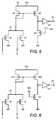
supply node 28 is connected direct to the positive voltage supply VCC. This embodiment is applicable where it can be ensured that all of the inputs are off when a low current state must be achieved. - Referring now to Figure 6, a fifth embodiment is similar to that described with respect to Figure 5, save that the output pull-
down transistor 24 is the same size as each of the input pull-down transistors 10-13, the necessary ratio between the currents being formed using the transistors of the current mirror. To that effect, the width of the diode-connectedcontrolling p FET 221 is half that of the controlledoutput p FET 222. - Referring to Figure 7, a sixth embodiment is shown in which the logic function is different to that achieved with the remaining embodiments. It will be seen to that end that each of the
transistors series transistors input 101 AND 102, OR 103 AND 104 are logic one. It will be clear to those skilled in the art that many other logic relationships can be achieved.
Claims (13)
- A logic gate comprising a current mirror circuit having a supply node, a first node and a second node wherein application of a first current at the first node causes a second current at the second node, plural input pull-down transistors connected between a reference node and one of said first and second nodes, and an output pull-down transistor connected between the other of said first and second nodes, and the reference terminal wherein the supply node has a connection to a supply terminal, the plural input pull-down transistors have respective control terminals connected to a corresponding plurality of input terminals and the output pull-down transistor has circuitry connected to its control node for biasing it on wherein said input pull-down transistors are mutually substantially identical and wherein said output pull-down transistor is smaller than each said input pull-down transistor.
- A logic gate as claimed in claim 1 wherein said plural input transistors are connected to said first node.
- A logic gate as claimed in claim 1 or 2 wherein the current mirror circuit has a pair of FETs having a common drain/source connection as said supply node, and common gates, one of said pair having its source/drain connected to its gate and said first node, and the other of said pair having its source/drain as said second node.
- A logic circuit as claimed in any preceding claim further comprising an enable transistor coupled between said supply node and said supply terminal.
- A logic circuit as claimed in claim 6 wherein said enable transistor is a p FET.
- A logic gate as claimed in any preceding claim wherein each said pull-down transistor is an n FET and said pair of FETs are p FETs.
- A logic gate as claimed in claim 2 further comprising an enable transistor connected between said plural input pull-down transistors and said first node.
- A logic gate as claimed in claim 1 wherein said output pull-down transistor comprises an enable transistor in use selectively enabled by supplied an enabling signal at its control gate.
- A logic circuit as claimed in any preceding claim wherein said output pull-down transistor is substantially half the width of each input pull-down transistor.
- A logic gate comprising a current mirror circuit having a supply node, a first node and a second node wherein application of a first current at the first node causes a second current at the second node, plural input pull-down transistors connected between a reference node and one of said first and second nodes, and an output pull-down transistor connected between the other of said first and second nodes, and the reference terminal wherein the supply node has a connection to a supply terminal, the plural input pull-down transistors have respective control terminals connected to a corresponding plurality of input terminals and the output pull-down transistor has circuitry connected to its control node for biasing it on, wherein said input pull-down transistors are mutually substantially identical and said output pull-down transistor is substantially the same as each said input pull-down transistor and the current mirror has a non-unity ratio.
- A logic gate as claimed in any preceding claim wherein at least one input pull-down transistor is connected in series with a second input pull-down transistor.
- A logic gate as claimed in any preceding claim and further comprising a disabling transistor connected between said reference node and one of said first and second nodes.
- A logic gate as claimed in any preceding claim and further comprising an inverter having a circuit output, said inverter being connected to one of said first and second nodes.
Applications Claiming Priority (2)
| Application Number | Priority Date | Filing Date | Title |
|---|---|---|---|
| GB9920082 | 1999-08-24 | ||
| GBGB9920082.6A GB9920082D0 (en) | 1999-08-24 | 1999-08-24 | Logic gate |
Publications (1)
| Publication Number | Publication Date |
|---|---|
| EP1079526A1 true EP1079526A1 (en) | 2001-02-28 |
Family
ID=10859751
Family Applications (1)
| Application Number | Title | Priority Date | Filing Date |
|---|---|---|---|
| EP00303979A Withdrawn EP1079526A1 (en) | 1999-08-24 | 2000-05-11 | Logic gate |
Country Status (3)
| Country | Link |
|---|---|
| US (1) | US6404238B1 (en) |
| EP (1) | EP1079526A1 (en) |
| GB (1) | GB9920082D0 (en) |
Families Citing this family (1)
| Publication number | Priority date | Publication date | Assignee | Title |
|---|---|---|---|---|
| US7265529B2 (en) * | 2004-08-19 | 2007-09-04 | Micron Technologgy, Inc. | Zero power start-up circuit |
Citations (3)
| Publication number | Priority date | Publication date | Assignee | Title |
|---|---|---|---|---|
| US4704544A (en) * | 1986-04-22 | 1987-11-03 | Unisearch Limited | Complementary current mirror logic |
| US5039886A (en) * | 1989-05-26 | 1991-08-13 | Nec Corporation | Current mirror type level converters |
| JPH0536280A (en) * | 1991-08-01 | 1993-02-12 | Seiko Epson Corp | Semiconductor integrated device |
Family Cites Families (2)
| Publication number | Priority date | Publication date | Assignee | Title |
|---|---|---|---|---|
| JPS62154917A (en) * | 1985-12-27 | 1987-07-09 | Hitachi Ltd | digital circuit |
| US4797580A (en) * | 1987-10-29 | 1989-01-10 | Northern Telecom Limited | Current-mirror-biased pre-charged logic circuit |
-
1999
- 1999-08-24 GB GBGB9920082.6A patent/GB9920082D0/en not_active Ceased
-
2000
- 2000-05-11 EP EP00303979A patent/EP1079526A1/en not_active Withdrawn
- 2000-08-21 US US09/643,065 patent/US6404238B1/en not_active Expired - Lifetime
Patent Citations (3)
| Publication number | Priority date | Publication date | Assignee | Title |
|---|---|---|---|---|
| US4704544A (en) * | 1986-04-22 | 1987-11-03 | Unisearch Limited | Complementary current mirror logic |
| US5039886A (en) * | 1989-05-26 | 1991-08-13 | Nec Corporation | Current mirror type level converters |
| JPH0536280A (en) * | 1991-08-01 | 1993-02-12 | Seiko Epson Corp | Semiconductor integrated device |
Non-Patent Citations (1)
| Title |
|---|
| PATENT ABSTRACTS OF JAPAN vol. 017, no. 329 (P - 1561) 22 June 1993 (1993-06-22) * |
Also Published As
| Publication number | Publication date |
|---|---|
| GB9920082D0 (en) | 1999-10-27 |
| US6404238B1 (en) | 2002-06-11 |
Similar Documents
| Publication | Publication Date | Title |
|---|---|---|
| KR100228951B1 (en) | Body voltage controlled semiconductor integrated circuit | |
| US4886984A (en) | Prohibition circuit upon power-on event | |
| US7176741B2 (en) | Level shift circuit | |
| US20070247210A1 (en) | Level shift circuit | |
| KR100310493B1 (en) | Ring oscillator and delay circuit | |
| US6137319A (en) | Reference-free single ended clocked sense amplifier circuit | |
| US6288591B1 (en) | Level shifter for multiple supply voltage circuitry | |
| US6404229B1 (en) | Complementary level shifting logic circuit with improved switching time | |
| JPH07105448B2 (en) | MOS integrated circuit | |
| US4717847A (en) | TTL compatible CMOS input buffer | |
| KR100218336B1 (en) | Level shifter | |
| US6753707B2 (en) | Delay circuit and semiconductor device using the same | |
| US5408145A (en) | Low power consumption and high speed NOR gate integrated circuit | |
| US6340907B2 (en) | Schmitt trigger circuit having independent threshold voltage setting to provide hysteresis | |
| US6057712A (en) | Integrated comparator circuit with four MOSFETS of defined transfer characteristics | |
| US5767696A (en) | Tri-state devices having exclusive gate output control | |
| US6404238B1 (en) | Ratio logic gate with a current mirror | |
| JP3540401B2 (en) | Level shift circuit | |
| KR0132782B1 (en) | Push-pull output circuit | |
| US6335649B1 (en) | Schmitt trigger circuit | |
| US5898320A (en) | Programmable interconnect point having reduced crowbar current | |
| EP1168624B1 (en) | CMOS bus driver circuit | |
| JP3927312B2 (en) | Input amplifier | |
| KR100361901B1 (en) | Circuit arrangement for reducing disturbances on account of the switching of an output driver | |
| KR100223827B1 (en) | Programmable Output Buffer Circuit |
Legal Events
| Date | Code | Title | Description |
|---|---|---|---|
| PUAI | Public reference made under article 153(3) epc to a published international application that has entered the european phase |
Free format text: ORIGINAL CODE: 0009012 |
|
| AK | Designated contracting states |
Kind code of ref document: A1 Designated state(s): DE FR GB IT |
|
| AX | Request for extension of the european patent |
Free format text: AL;LT;LV;MK;RO;SI |
|
| 17P | Request for examination filed |
Effective date: 20010816 |
|
| AKX | Designation fees paid |
Free format text: DE FR GB IT |
|
| 17Q | First examination report despatched |
Effective date: 20080131 |
|
| STAA | Information on the status of an ep patent application or granted ep patent |
Free format text: STATUS: THE APPLICATION IS DEEMED TO BE WITHDRAWN |
|
| 18D | Application deemed to be withdrawn |
Effective date: 20080812 |