EP1079519A1 - A power rising electronic device - Google Patents
A power rising electronic device Download PDFInfo
- Publication number
- EP1079519A1 EP1079519A1 EP00202920A EP00202920A EP1079519A1 EP 1079519 A1 EP1079519 A1 EP 1079519A1 EP 00202920 A EP00202920 A EP 00202920A EP 00202920 A EP00202920 A EP 00202920A EP 1079519 A1 EP1079519 A1 EP 1079519A1
- Authority
- EP
- European Patent Office
- Prior art keywords
- terminal
- current
- output
- voltage
- input
- Prior art date
- Legal status (The legal status is an assumption and is not a legal conclusion. Google has not performed a legal analysis and makes no representation as to the accuracy of the status listed.)
- Granted
Links
- 230000000630 rising effect Effects 0.000 title claims abstract description 14
- 238000012886 linear function Methods 0.000 claims abstract description 11
- 238000000034 method Methods 0.000 claims description 4
- 230000009977 dual effect Effects 0.000 claims description 2
- 239000000463 material Substances 0.000 description 3
- 239000004065 semiconductor Substances 0.000 description 3
- 230000001419 dependent effect Effects 0.000 description 1
- 238000010586 diagram Methods 0.000 description 1
- 230000005669 field effect Effects 0.000 description 1
- 238000012986 modification Methods 0.000 description 1
- 230000004048 modification Effects 0.000 description 1
- 230000003068 static effect Effects 0.000 description 1
Images


Classifications
-
- H—ELECTRICITY
- H03—ELECTRONIC CIRCUITRY
- H03F—AMPLIFIERS
- H03F3/00—Amplifiers with only discharge tubes or only semiconductor devices as amplifying elements
- H03F3/34—DC amplifiers in which all stages are DC-coupled
- H03F3/343—DC amplifiers in which all stages are DC-coupled with semiconductor devices only
- H03F3/345—DC amplifiers in which all stages are DC-coupled with semiconductor devices only with field-effect devices
-
- G—PHYSICS
- G05—CONTROLLING; REGULATING
- G05F—SYSTEMS FOR REGULATING ELECTRIC OR MAGNETIC VARIABLES
- G05F3/00—Non-retroactive systems for regulating electric variables by using an uncontrolled element, or an uncontrolled combination of elements, such element or such combination having self-regulating properties
- G05F3/02—Regulating voltage or current
- G05F3/08—Regulating voltage or current wherein the variable is DC
- G05F3/10—Regulating voltage or current wherein the variable is DC using uncontrolled devices with non-linear characteristics
- G05F3/16—Regulating voltage or current wherein the variable is DC using uncontrolled devices with non-linear characteristics being semiconductor devices
- G05F3/20—Regulating voltage or current wherein the variable is DC using uncontrolled devices with non-linear characteristics being semiconductor devices using diode- transistor combinations
- G05F3/26—Current mirrors
- G05F3/267—Current mirrors using both bipolar and field-effect technology
Definitions
- the present invention relates to a power rising electronic device.
- Power rising electronic devices are commonly used in various applications such as, for example, in analog calculating systems.
- a power rising electronic device can provide an output current which is a function of a power of an input current with a relative whole-number (either positive or negative) exponent; in particular, in the case of a square law electronic device, the output current is proportional to the square of the input current.
- a different known solution consists of the use of one or more MOS field effect transistors in which the current at the drain terminal is proportional to the square of the voltage between the source terminal and the gate terminal.
- this relationship is influenced to a fairly marked extent by variations in temperature and in the drain terminal voltage, so that the electronic device is not very precise.
- the object of the present invention is to overcome the above-mentioned drawbacks.
- a power rising electronic device as described in the first claim is proposed.
- a power rising electronic device for receiving an input current and for supplying an output current which is a linear function of a power of the input current with a relative whole-number exponent, comprising a number of diodes equal to the absolute value of the relative whole-number exponent, connected in series with one another so as to produce, from the input current, an input voltage which is a logarithmic function of a power of the input current with an exponent equal ,to said absolute value, an output junction element, and means for applying a voltage which is a linear function of the input voltage to the output junction element so as to produce a current which is an exponential function of the voltage applied, the output current being derived from the current in the output junction element.
- this shows a square law electronic device 100a, produced in integrated form in a chip of semiconductor material with the use of a bipolar-CMOS (or BICMOS) technique.
- the electronic device 100a has two supply terminals 105g and 105v.
- the supply terminal 105g is connected to a reference terminal (or ground); the supply terminal 105v is connected to the positive terminal of a direct-current supply +Vdd (for example, a 5V supply), the negative terminal of which is connected to the ground terminal.
- the electronic device 100a also has an input terminal 105i which receives an input current Ii, an output terminal 105o which supplies an output current Io, and a reference terminal 105r which receives a reference current Ir of predetermined value.
- Two diodes Di1 and Di2 are connected in series between the input terminal 105i and the supply terminal 105g.
- the anode terminal of the diode Di1 is connected to the input terminal 105i;
- the cathode terminal of the diode Di1 is connected to the anode terminal of the diode Di2, the cathode terminal of which is connected to the supply terminal 105g.
- a further diode Dr has its anode terminal connected to the reference terminal 105r and its cathode terminal connected to the supply terminal 105g.
- the electronic device 100a also includes a pnp bipolar transistor Ti having its base terminal connected to the input terminal 105i and its collector terminal connected to the supply terminal 105g.
- a further pnp bipolar transistor Tr has its base terminal connected to the reference terminal 105r and its collector terminal connected to the supply terminal 105g.
- a dual current-mirror with a cascode structure is formed by six p-channel MOS transistors M1, M2, M3, M4, M5, and M6; the current-mirror M1-M6 has an input branch M1, M2 connected to the collector terminal of the transistor To, a first output branch M3, M4, connected to the emitter terminal of the transistor Ti, and a second output branch M5, M6 connected to the output terminal 105o.
- the drain terminal of the transistor M1 is connected to the collector terminal of the transistor To; the source terminal of the transistor M1 is connected to the drain terminal of the transistor M2, the source terminal of which is connected to the supply terminal 105v.
- the gate terminals of the transistors M1 and M2 are short-circuited to their respective drain terminals.
- the drain terminal of the transistor M3 is connected to the emitter terminal of the transistor Ti; the source terminal of the transistor M3 is connected to the drain terminal of the transistor M4, the source terminal of which is connected to the supply terminal 105v.
- the drain terminal of the transistor M5 is connected to the output terminal 105o; the source terminal of the transistor M5 is connected to the drain terminal of the transistor M6, the source terminal of which is connected to the supply terminal 105v.
- the gate terminals of the transistors M3, M5 and of the transistors M4, M6 are connected to the gate terminals of the transistors M1 and M2, respectively.
- the current through the diodes Di1 and Di2 is equal to the input current Ii.
- the output current Io is thus proportional to the square of the input current Ii.
- a single diode Di is connected between the input terminal 105i and the supply terminal 105g and two diodes Dr1 and Dr2 are connected in series between the reference terminal 105r and the supply terminal 105g.
- the transistor To has its base terminal connected to the emitter terminal of the transistor Tr and its emitter terminal connected to the emitter terminal of the transistor Ti.
- the output current Io is thus a hyperbolic function of the input current Ii (that is, their product is constant).
- the arrangement according to the present invention provides a power rising electronic device in which the output current is a linear function of a power of the input current with a relative whole-number (that is, positive or negative) exponent.
- One or more diodes are connected in series with one another to produce, from the input current, an input voltage which is a logarithmic function of an Nth power of the input current.
- the electronic device includes an output junction element to which a voltage which is a linear function of the input voltage is applied so as to produce a current which is an exponential function of the voltage applied, and from which the output current is obtained.
- the arrangement of the present invention is extremely simple.
- the electronic device is particularly compact and occupies a limited amount of space on the chip of semiconductor material (when it is produced in integrated form).
- the electronic device according to the present invention is very accurate and stable since it is affected in very limited manner by temperature variations.
- the output current is independent of the supply voltage so that the electronic device has very high supply-voltage noise rejection.
- the diode Dr and the reference current Ir produce a voltage Vbeo which is directly proportional, in accordance with the thermal voltage Vt, to the logarithmic term having the square of the input current Ii as its argument.
- the term Vt which is greatly dependent on temperature, thus disappears from the formula which defines the output current Io.
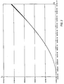
- Figure 2 shows, by way of example, the curve of the output current Io as a function of the input current Ii, with the reference current Ir set at 40 ⁇ A. In particular, several curves of the output current Io at various temperatures between 20°C and 90°C are shown. As can be seen, the output current Io is substantially independent of the temperature. Moreover, the output current Io is directly proportional to the square of the input current Ii (without any linear component).
- the voltage Vbeo has a value such as to permit correct biasing of the transistor To.
- the number of diodes (Dr) connected to the reference terminal 105r is, in general, equal to the number of diodes (Di1, Di2) connected to the input terminal 105i minus one
- the number of diodes (Dr1, Dr1) connected to the reference terminal 105r is equal to the number of diodes (Di) connected to the input terminal 105i plus one.
- the transistors Ti and Tr are used to decouple the diodes Di1, Di2 and Dr, respectively, from the transistor To, so that the input current Ii and the reference current Ir flow entirely through the corresponding diodes Di1, Di2 and Dr.
- the transistors Ti, Tr also operate as voltage translators for biasing the transistor To.
- the current-mirror M1-M6 decouples the transistor To from a load (not shown in the drawing) connected to the output terminal 105o; the output current Io is thus substantially independent of an output voltage at the terminals of the load. Moreover, the cascode structure of the current-mirror M1-M6 ensures great accuracy of the mirror factor.
- the electronic device of the present invention may, in any case, also be formed with other means for applying a voltage which is a linear function of the voltage Vi between the base terminal and the emitter terminal of the transistor To, or with other means for deriving the output current Io from the current Ic (or even a simple connection between the collector terminal of the transistor To and the output terminal 105o).
Landscapes
- Engineering & Computer Science (AREA)
- Physics & Mathematics (AREA)
- Microelectronics & Electronic Packaging (AREA)
- Nonlinear Science (AREA)
- Electromagnetism (AREA)
- General Physics & Mathematics (AREA)
- Radar, Positioning & Navigation (AREA)
- Automation & Control Theory (AREA)
- Power Engineering (AREA)
- Amplifiers (AREA)
- Control Of Electrical Variables (AREA)
Abstract
Description
- The present invention relates to a power rising electronic device.
- Power rising electronic devices are commonly used in various applications such as, for example, in analog calculating systems. A power rising electronic device can provide an output current which is a function of a power of an input current with a relative whole-number (either positive or negative) exponent; in particular, in the case of a square law electronic device, the output current is proportional to the square of the input current.
- Power rising electronic devices are formed with the use of one of more multiplier circuits. A disadvantage of this solution is that it requires a fairly complex structure; if the electronic device is produced in integrated form in a chip of semiconductor material, this leads to the occupation of a considerable amount of space. Moreover, multiplier circuits require very precise tuning of the components used to prevent drift of the output current, for example, due to temperature variations.
- A different known solution consists of the use of one or more MOS field effect transistors in which the current at the drain terminal is proportional to the square of the voltage between the source terminal and the gate terminal. However, this relationship is influenced to a fairly marked extent by variations in temperature and in the drain terminal voltage, so that the electronic device is not very precise.
- The object of the present invention is to overcome the above-mentioned drawbacks. In order to achieve this object, a power rising electronic device as described in the first claim is proposed.
- In short, there is provided a power rising electronic device for receiving an input current and for supplying an output current which is a linear function of a power of the input current with a relative whole-number exponent, comprising a number of diodes equal to the absolute value of the relative whole-number exponent, connected in series with one another so as to produce, from the input current, an input voltage which is a logarithmic function of a power of the input current with an exponent equal ,to said absolute value, an output junction element, and means for applying a voltage which is a linear function of the input voltage to the output junction element so as to produce a current which is an exponential function of the voltage applied, the output current being derived from the current in the output junction element.
- A corresponding power rising method is also proposed.
- Further characteristics and the advantages of the power rising electronic device according to the present invention will become clear from the following description of a preferred embodiment thereof, provided by way of non-limiting example, with reference to the appended drawings, in which:
- Figure 1a is a basic circuit diagram of the electronic device,
- Figure 1b shows a different embodiment of the electronic device,
- Figure 2 shows the curve of the output current as a function of the input current at various temperatures, for the electronic device of Figure 1a.
-
- With reference in particular to Figure 1a, this shows a square law electronic device 100a, produced in integrated form in a chip of semiconductor material with the use of a bipolar-CMOS (or BICMOS) technique. The electronic device 100a has two supply terminals 105g and 105v. The supply terminal 105g is connected to a reference terminal (or ground); the supply terminal 105v is connected to the positive terminal of a direct-current supply +Vdd (for example, a 5V supply), the negative terminal of which is connected to the ground terminal. The electronic device 100a also has an input terminal 105i which receives an input current Ii, an output terminal 105o which supplies an output current Io, and a reference terminal 105r which receives a reference current Ir of predetermined value.
- Two diodes Di1 and Di2 are connected in series between the input terminal 105i and the supply terminal 105g. In particular, the anode terminal of the diode Di1 is connected to the input terminal 105i; the cathode terminal of the diode Di1 is connected to the anode terminal of the diode Di2, the cathode terminal of which is connected to the supply terminal 105g. A further diode Dr has its anode terminal connected to the reference terminal 105r and its cathode terminal connected to the supply terminal 105g.
- The electronic device 100a also includes a pnp bipolar transistor Ti having its base terminal connected to the input terminal 105i and its collector terminal connected to the supply terminal 105g. A further pnp bipolar transistor Tr has its base terminal connected to the reference terminal 105r and its collector terminal connected to the supply terminal 105g. In the electronic device 100a, there is also an npn bipolar transistor To having its base terminal connected to the emitter terminal of the transistor Ti and its emitter terminal connected to the emitter terminal of the transistor Tr.
- A dual current-mirror with a cascode structure is formed by six p-channel MOS transistors M1, M2, M3, M4, M5, and M6; the current-mirror M1-M6 has an input branch M1, M2 connected to the collector terminal of the transistor To, a first output branch M3, M4, connected to the emitter terminal of the transistor Ti, and a second output branch M5, M6 connected to the output terminal 105o.
- In particular, the drain terminal of the transistor M1 is connected to the collector terminal of the transistor To; the source terminal of the transistor M1 is connected to the drain terminal of the transistor M2, the source terminal of which is connected to the supply terminal 105v. The gate terminals of the transistors M1 and M2 are short-circuited to their respective drain terminals. The drain terminal of the transistor M3 is connected to the emitter terminal of the transistor Ti; the source terminal of the transistor M3 is connected to the drain terminal of the transistor M4, the source terminal of which is connected to the supply terminal 105v. Similarly, the drain terminal of the transistor M5 is connected to the output terminal 105o; the source terminal of the transistor M5 is connected to the drain terminal of the transistor M6, the source terminal of which is connected to the supply terminal 105v. The gate terminals of the transistors M3, M5 and of the transistors M4, M6 are connected to the gate terminals of the transistors M1 and M2, respectively.
- If the base current of the transistor Ti is considered negligible, the current through the diodes Di1 and Di2 is equal to the input current Ii. From the equation which defines the relation between the voltage and the current in a generic pn junction:
- The voltage Vi at the terminals of the series of diodes Di1 and Di2 is thus:
- Similarly, if the base current of the transistor Tr is ignored and the inverse saturation current of the diode Dr is indicated Isr, the voltage Vr at the terminals of the diode Dr is:
- Now, the base-emitter voltages of the transistors Ti and Tr will be indicated Vbei and Vber, respectively. If the voltages Vbei and Vber are considered substantially equal to one another, the base-emitter voltage Vbeo of the transistor To is equal to:
- With similar considerations applied to the transistor To, if the base and collector currents are indicated Ib and Ic, respectively, if the static current gain is indicated hfe, and if the inverse saturation current of the base-emitter junction is indicated Iso:
- The current Ic is mirrored by the structure M1, M2, M5, M6 towards the output terminal 105o (with the branch M3, M4 operating as an active load of the transistor Ti) so that:
- In particular, upon the assumption that
- The output current Io is thus proportional to the square of the input current Ii.
- Alternatively, as shown in Figure 1b (elements corresponding to those shown in the previous drawing are identified by the same reference numerals or symbols and an explanation thereof is omitted for simplicity of description), an electronic device 100b with a hyperbolic law is provided.
- In this case, a single diode Di is connected between the input terminal 105i and the supply terminal 105g and two diodes Dr1 and Dr2 are connected in series between the reference terminal 105r and the supply terminal 105g. The transistor To has its base terminal connected to the emitter terminal of the transistor Tr and its emitter terminal connected to the emitter terminal of the transistor Ti.
- By similar considerations to those given above:
- The output current Io is thus equal to:
- In particular, upon the assumption that
- The output current Io is thus a hyperbolic function of the input current Ii (that is, their product is constant).
- Similar considerations apply if the electronic device is produced by a different technique or is not in integrated form, if equivalent circuit arrangements are used, for example, with the output transistor To replaced by a different junction element, if the various diodes are formed by bipolar transistors, if the transistors Ti, Tr are of npn type and the transistor To is of pnp type, if the load of the transistor Ti is constituted by a resistor, etc.
- More generally, the arrangement according to the present invention provides a power rising electronic device in which the output current is a linear function of a power of the input current with a relative whole-number (that is, positive or negative) exponent. One or more diodes, the number of diodes being equal to the absolute value N of the exponent, are connected in series with one another to produce, from the input current, an input voltage which is a logarithmic function of an Nth power of the input current. The electronic device includes an output junction element to which a voltage which is a linear function of the input voltage is applied so as to produce a current which is an exponential function of the voltage applied, and from which the output current is obtained.
- The arrangement of the present invention is extremely simple. The electronic device is particularly compact and occupies a limited amount of space on the chip of semiconductor material (when it is produced in integrated form).
- The electronic device according to the present invention is very accurate and stable since it is affected in very limited manner by temperature variations.
- Moreover, the output current is independent of the supply voltage so that the electronic device has very high supply-voltage noise rejection.
- In the particular embodiment of the present invention shown in Figure 1a (similar considerations apply to the electronic device of Figure 1b), the diode Dr and the reference current Ir produce a voltage Vbeo which is directly proportional, in accordance with the thermal voltage Vt, to the logarithmic term having the square of the input current Ii as its argument. The term Vt, which is greatly dependent on temperature, thus disappears from the formula which defines the output current Io. Figure 2 shows, by way of example, the curve of the output current Io as a function of the input current Ii, with the reference current Ir set at 40µA. In particular, several curves of the output current Io at various temperatures between 20°C and 90°C are shown. As can be seen, the output current Io is substantially independent of the temperature. Moreover, the output current Io is directly proportional to the square of the input current Ii (without any linear component).
- These elements also ensure that the voltage Vbeo has a value such as to permit correct biasing of the transistor To. In particular, in the embodiment shown in Figure 1a (in which the voltage Vbeo is equal to the difference between the voltage Vi and the voltage Vr), the number of diodes (Dr) connected to the reference terminal 105r is, in general, equal to the number of diodes (Di1, Di2) connected to the input terminal 105i minus one, whereas in the embodiment shown in Figure 1b (in which the voltage Vbeo is equal to the difference between the voltage Vr and the voltage Vi), the number of diodes (Dr1, Dr1) connected to the reference terminal 105r is equal to the number of diodes (Di) connected to the input terminal 105i plus one.
- The transistors Ti and Tr are used to decouple the diodes Di1, Di2 and Dr, respectively, from the transistor To, so that the input current Ii and the reference current Ir flow entirely through the corresponding diodes Di1, Di2 and Dr. The transistors Ti, Tr also operate as voltage translators for biasing the transistor To.
- The current-mirror M1-M6 decouples the transistor To from a load (not shown in the drawing) connected to the output terminal 105o; the output current Io is thus substantially independent of an output voltage at the terminals of the load. Moreover, the cascode structure of the current-mirror M1-M6 ensures great accuracy of the mirror factor.
- Similar considerations apply if a different number of diodes is connected to the input terminal and to the reference terminal, if other equivalent means are provided for supplying a reference voltage, if the transistors Ti and Tr are replaced by other decoupling elements, if the current-mirror does not have a cascode structure, etc. The electronic device of the present invention may, in any case, also be formed with other means for applying a voltage which is a linear function of the voltage Vi between the base terminal and the emitter terminal of the transistor To, or with other means for deriving the output current Io from the current Ic (or even a simple connection between the collector terminal of the transistor To and the output terminal 105o).
- Naturally, in order to satisfy contingent and specific requirements, an expert in the art may apply to the above-described power rising electronic device many modifications and variations all of which, however, are included within the scope of protection of the invention as defined by the following claims.
Claims (10)
- A power rising electronic device (100a; 100b) for receiving an input current (Ii) and for supplying an output current (Io) which is a linear function of a power of the input current (Ii) with a relative whole-number exponent,
characterized in that
it includes a number of diodes (Di1, Di2; Di) equal to the absolute value of the relative whole-number exponent, connected in series with one another so as to produce, from the input current (Ii), an input voltage (Vi) which is a logarithmic function of a power of the input current (Ii) with an exponent equal to said absolute value, an output junction element (To), and means (105r, Dr, Ti, Tr; 105r, Dr1, Dr2, Ti, Tr) for applying a voltage (Vbeo) which is a linear function of the input voltage (Vi) to the output junction element (To) so as to produce a current (Ic) which is an exponential function of the voltage (Vbeo) applied, the output current (Io) being derived from the current in the output junction element (Ic). - An electronic device (100a; 100b) according to Claim 1, in which the output junction element is an output bipolar transistor (To), the voltage applied being a base-emitter voltage (Vbeo) and the current in the output junction element being a collector current (Ic).
- An electronic device (100a; 100b) according to Claim 2, further comprising reference means (105r, Dr; 105r, Dr1, Dr2) for supplying a reference voltage (Vr), the base-emitter voltage (Vbeo) being equal to the difference between the input voltage (Vi) and the reference voltage (Vr), or vice versa.
- An electronic device (100a; 100b) according to Claim 3, further comprising an input terminal (105i) for receiving the input current (Ii) and a supply terminal (105g), the diodes (Di1, Di2; Di) being connected between the input terminal (105i) and the supply terminal (105g), and in which the reference means (105r, Dr; 105r, Dr1, Dr2) include a reference terminal (105r) for receiving a reference current (Ir) and a number of further diodes (Dr; Dr1, Dr2) equal to said absolute value minus one if the base-emitter voltage (Vbeo) is equal to the difference between the input voltage (Vi) and the reference voltage (Vr), or equal to said absolute value plus one if the base-emitter voltage (Vbeo) is equal to the difference between the reference voltage (Vr) and the input voltage (Vi), in which the further diodes (Dr; Dr1, Dr2) are connected in series between the reference terminal (105r) and the supply terminal (105g) for obtaining the reference voltage (Vr) from the reference current (Ir), the reference voltage (Vr) being a logarithmic function of a power of the reference current (Ir) with an exponent equal to the number of further diodes (Dr; Dr1, Dr2).
- An electronic device (100a; 100b) according to Claim 4, further comprising a first decoupling element (Ti) connected between the input terminal (105i) and a first of the base terminal and the emitter terminal of the output transistor (To), and a second decoupling element (Tr) connected between the reference terminal (105r) and a second different of the base terminal and the emitter terminal of the output transistor (To).
- An electronic device (100a; 100b) according to Claim 5, in which the first decoupling element and the second decoupling element include, respectively, a first bipolar transistor (Ti) and a second bipolar transistor (Tr) having a polarity (pnp) opposite to a polarity (npn) of the output transistor (To), the first transistor (Ti) having an emitter terminal connected to the first terminal of the output transistor (To), a base terminal connected to the input terminal (105i) and a collector terminal connected to the supply terminal (105g), and the second transistor (Tr) having an emitter terminal connected to the second terminal of the output transistor (To), a base terminal connected to the reference terminal (105r), and a collector terminal connected to the supply terminal (105g).
- An electronic device (100a; 100b) according to any one of Claims 1 to 6, further comprising an output terminal (105o) for supplying the output current (Io) and a current-mirror (M1-M6) connected between a collector terminal of the output transistor (To) and the output terminal (105o), the output current (Io) being equal to the collector current (Ic).
- An electronic device (100a; 100b) according to Claim 7, in which the current-mirror (M1-M6) has a cascode structure.
- An electronic device (100a; 100b) according to Claim 7 or Claim 8, in which the current-mirror (M1-M6) is a dual current-mirror with an input branch (M1, M2) connected between the collector terminal of the output transistor (To) and a further supply terminal (105v), a first output branch (M3, M4) connected between the base terminal of the output transistor (To) and the further supply terminal (105v), and a second output branch (M5, M6) connected between the output terminal (105o) and the further supply terminal (105v).
- A power rising method comprising the steps of:receiving an input current (Ii), andsupplying an output current (Io) which is a linear function of a power of the input current (Ii) with a relative whole-number exponent,
characterized by the steps ofobtaining from the input current (Ii) an input voltage (Vi) which is a logarithmic function of a power of the input current (Ii) with an exponent equal to the absolute value of the relative whole-number exponent, by means of a number of diodes (Di1, Di2; Di) equal to said absolute value connected in series with one another,applying a voltage (Vbeo) which is a linear function of the input voltage (Vi) to an output junction element (To) so as to obtain a current (Ic) which is an exponential function of the voltage (Vbeo) applied, andderiving the output current (Io) from the current in the output junction element (Ic).
Applications Claiming Priority (2)
| Application Number | Priority Date | Filing Date | Title |
|---|---|---|---|
| US382244 | 1989-07-19 | ||
| US09/382,244 US6215292B1 (en) | 1999-08-25 | 1999-08-25 | Method and device for generating an output current |
Publications (2)
| Publication Number | Publication Date |
|---|---|
| EP1079519A1 true EP1079519A1 (en) | 2001-02-28 |
| EP1079519B1 EP1079519B1 (en) | 2008-07-09 |
Family
ID=23508116
Family Applications (1)
| Application Number | Title | Priority Date | Filing Date |
|---|---|---|---|
| EP00202920A Expired - Lifetime EP1079519B1 (en) | 1999-08-25 | 2000-08-21 | A power rising electronic device |
Country Status (3)
| Country | Link |
|---|---|
| US (1) | US6215292B1 (en) |
| EP (1) | EP1079519B1 (en) |
| DE (1) | DE60039391D1 (en) |
Families Citing this family (4)
| Publication number | Priority date | Publication date | Assignee | Title |
|---|---|---|---|---|
| DE102004046349A1 (en) * | 2004-09-24 | 2006-04-06 | Infineon Technologies Ag | Logarithmberschaltung and highly linear differential amplifier circuit |
| US7546332B2 (en) * | 2004-11-09 | 2009-06-09 | Theta Microelectronics, Inc. | Apparatus and methods for implementation of mathematical functions |
| GB2427475B (en) * | 2005-06-20 | 2008-07-09 | Radiodetection Ltd | A detector for detecting a buried current carrying conductor |
| FR3032309B1 (en) * | 2015-02-02 | 2017-06-23 | St Microelectronics Alps Sas | VOLTAGE CONTROL CIRCUIT FOR STRONG AND LOW POWER |
Citations (4)
| Publication number | Priority date | Publication date | Assignee | Title |
|---|---|---|---|---|
| GB1465499A (en) * | 1973-08-09 | 1977-02-23 | Rca Corp | Current amplifier |
| US5602509A (en) * | 1994-06-09 | 1997-02-11 | Nec Corporation | MOS operational transconductance amplifier using an adaptively-biased differential pair |
| US5712594A (en) * | 1995-05-31 | 1998-01-27 | Nec Corporation | Operational transconductance amplifier operable at low supply voltage |
| US5831327A (en) * | 1919-12-13 | 1998-11-03 | Nec Corporation | Differential circuit with a dynamic bias current for producing an exponential or a square-law transfer characteristic |
Family Cites Families (6)
| Publication number | Priority date | Publication date | Assignee | Title |
|---|---|---|---|---|
| JP2837080B2 (en) * | 1993-11-16 | 1998-12-14 | シャープ株式会社 | Multiplication circuit |
| US5835994A (en) * | 1994-06-30 | 1998-11-10 | Adams; William John | Cascode current mirror with increased output voltage swing |
| US5585757A (en) * | 1995-06-06 | 1996-12-17 | Analog Devices, Inc. | Explicit log domain root-mean-square detector |
| US5680038A (en) * | 1996-06-20 | 1997-10-21 | Lsi Logic Corporation | High-swing cascode current mirror |
| KR0183549B1 (en) * | 1996-07-10 | 1999-04-15 | 정명식 | Temperature independent current source |
| KR100219037B1 (en) * | 1996-10-01 | 1999-09-01 | 이계철 | FET resistance based analogue multiplier |
-
1999
- 1999-08-25 US US09/382,244 patent/US6215292B1/en not_active Expired - Lifetime
-
2000
- 2000-08-21 DE DE60039391T patent/DE60039391D1/en not_active Expired - Lifetime
- 2000-08-21 EP EP00202920A patent/EP1079519B1/en not_active Expired - Lifetime
Patent Citations (4)
| Publication number | Priority date | Publication date | Assignee | Title |
|---|---|---|---|---|
| US5831327A (en) * | 1919-12-13 | 1998-11-03 | Nec Corporation | Differential circuit with a dynamic bias current for producing an exponential or a square-law transfer characteristic |
| GB1465499A (en) * | 1973-08-09 | 1977-02-23 | Rca Corp | Current amplifier |
| US5602509A (en) * | 1994-06-09 | 1997-02-11 | Nec Corporation | MOS operational transconductance amplifier using an adaptively-biased differential pair |
| US5712594A (en) * | 1995-05-31 | 1998-01-27 | Nec Corporation | Operational transconductance amplifier operable at low supply voltage |
Also Published As
| Publication number | Publication date |
|---|---|
| DE60039391D1 (en) | 2008-08-21 |
| US6215292B1 (en) | 2001-04-10 |
| EP1079519B1 (en) | 2008-07-09 |
Similar Documents
| Publication | Publication Date | Title |
|---|---|---|
| US9898030B2 (en) | Fractional bandgap reference voltage generator | |
| US5670907A (en) | VBB reference for pumped substrates | |
| US6661713B1 (en) | Bandgap reference circuit | |
| US4329639A (en) | Low voltage current mirror | |
| US9276571B2 (en) | Systems and methods for driving transistors with high threshold voltages | |
| US9489004B2 (en) | Bandgap reference voltage generator circuits | |
| US6242897B1 (en) | Current stacked bandgap reference voltage source | |
| US4763028A (en) | Circuit and method for semiconductor leakage current compensation | |
| US4931718A (en) | CMOS voltage reference | |
| CN115525090A (en) | Method, system and apparatus for generating a compensated voltage reference | |
| US5187395A (en) | BIMOS voltage bias with low temperature coefficient | |
| US7675353B1 (en) | Constant current and voltage generator | |
| EP0352044B1 (en) | Transistor base current compensation circuitry | |
| US20200336141A1 (en) | Supply voltage supervisor | |
| EP1079519B1 (en) | A power rising electronic device | |
| US4602207A (en) | Temperature and power supply stable current source | |
| EP0443239A1 (en) | Current mirror with base current compensation | |
| US20200264647A1 (en) | Current reference circuit | |
| US6605987B2 (en) | Circuit for generating a reference voltage based on two partial currents with opposite temperature dependence | |
| US6809575B2 (en) | Temperature-compensated current reference circuit | |
| US6480038B1 (en) | Bipolar comparator | |
| US20070200546A1 (en) | Reference voltage generating circuit for generating low reference voltages | |
| US4577119A (en) | Trimless bandgap reference voltage generator | |
| JP3349047B2 (en) | Constant voltage circuit | |
| US4634959A (en) | Temperature compensated reference circuit |
Legal Events
| Date | Code | Title | Description |
|---|---|---|---|
| PUAI | Public reference made under article 153(3) epc to a published international application that has entered the european phase |
Free format text: ORIGINAL CODE: 0009012 |
|
| AK | Designated contracting states |
Kind code of ref document: A1 Designated state(s): DE FR GB IT |
|
| AX | Request for extension of the european patent |
Free format text: AL;LT;LV;MK;RO;SI |
|
| RAP1 | Party data changed (applicant data changed or rights of an application transferred) |
Owner name: HEWLETT-PACKARD COMPANY, A DELAWARE CORPORATION Owner name: STMICROELECTRONICS S.R.L. |
|
| 17P | Request for examination filed |
Effective date: 20010807 |
|
| AKX | Designation fees paid |
Free format text: DE FR GB IT |
|
| GRAP | Despatch of communication of intention to grant a patent |
Free format text: ORIGINAL CODE: EPIDOSNIGR1 |
|
| RIN1 | Information on inventor provided before grant (corrected) |
Inventor name: GHOZEIL, ADAM Inventor name: MAGGI, RICCARDO |
|
| GRAS | Grant fee paid |
Free format text: ORIGINAL CODE: EPIDOSNIGR3 |
|
| GRAA | (expected) grant |
Free format text: ORIGINAL CODE: 0009210 |
|
| AK | Designated contracting states |
Kind code of ref document: B1 Designated state(s): DE FR GB IT |
|
| REG | Reference to a national code |
Ref country code: GB Ref legal event code: FG4D |
|
| REF | Corresponds to: |
Ref document number: 60039391 Country of ref document: DE Date of ref document: 20080821 Kind code of ref document: P |
|
| PLBE | No opposition filed within time limit |
Free format text: ORIGINAL CODE: 0009261 |
|
| STAA | Information on the status of an ep patent application or granted ep patent |
Free format text: STATUS: NO OPPOSITION FILED WITHIN TIME LIMIT |
|
| 26N | No opposition filed |
Effective date: 20090414 |
|
| REG | Reference to a national code |
Ref country code: FR Ref legal event code: ST Effective date: 20090630 |
|
| PG25 | Lapsed in a contracting state [announced via postgrant information from national office to epo] |
Ref country code: IT Free format text: LAPSE BECAUSE OF FAILURE TO SUBMIT A TRANSLATION OF THE DESCRIPTION OR TO PAY THE FEE WITHIN THE PRESCRIBED TIME-LIMIT Effective date: 20080709 |
|
| PG25 | Lapsed in a contracting state [announced via postgrant information from national office to epo] |
Ref country code: FR Free format text: LAPSE BECAUSE OF NON-PAYMENT OF DUE FEES Effective date: 20080901 |
|
| PGFP | Annual fee paid to national office [announced via postgrant information from national office to epo] |
Ref country code: GB Payment date: 20120725 Year of fee payment: 13 |
|
| GBPC | Gb: european patent ceased through non-payment of renewal fee |
Effective date: 20130821 |
|
| PG25 | Lapsed in a contracting state [announced via postgrant information from national office to epo] |
Ref country code: GB Free format text: LAPSE BECAUSE OF NON-PAYMENT OF DUE FEES Effective date: 20130821 |
|
| PGFP | Annual fee paid to national office [announced via postgrant information from national office to epo] |
Ref country code: DE Payment date: 20190722 Year of fee payment: 20 |
|
| REG | Reference to a national code |
Ref country code: DE Ref legal event code: R071 Ref document number: 60039391 Country of ref document: DE |