EP1079513A1 - Oscillating apparatus including two-band resonance circuit - Google Patents
Oscillating apparatus including two-band resonance circuit Download PDFInfo
- Publication number
- EP1079513A1 EP1079513A1 EP00306530A EP00306530A EP1079513A1 EP 1079513 A1 EP1079513 A1 EP 1079513A1 EP 00306530 A EP00306530 A EP 00306530A EP 00306530 A EP00306530 A EP 00306530A EP 1079513 A1 EP1079513 A1 EP 1079513A1
- Authority
- EP
- European Patent Office
- Prior art keywords
- frequency band
- series resonance
- band
- emitter
- frequency
- Prior art date
- Legal status (The legal status is an assumption and is not a legal conclusion. Google has not performed a legal analysis and makes no representation as to the accuracy of the status listed.)
- Granted
Links
- 230000010355 oscillation Effects 0.000 claims abstract description 54
- 239000003990 capacitor Substances 0.000 claims description 21
- 239000004020 conductor Substances 0.000 claims description 14
- 230000003321 amplification Effects 0.000 abstract description 6
- 238000003199 nucleic acid amplification method Methods 0.000 abstract description 6
- 238000010586 diagram Methods 0.000 description 4
Images

Classifications
-
- H—ELECTRICITY
- H03—ELECTRONIC CIRCUITRY
- H03B—GENERATION OF OSCILLATIONS, DIRECTLY OR BY FREQUENCY-CHANGING, BY CIRCUITS EMPLOYING ACTIVE ELEMENTS WHICH OPERATE IN A NON-SWITCHING MANNER; GENERATION OF NOISE BY SUCH CIRCUITS
- H03B5/00—Generation of oscillations using amplifier with regenerative feedback from output to input
- H03B5/18—Generation of oscillations using amplifier with regenerative feedback from output to input with frequency-determining element comprising distributed inductance and capacitance
- H03B5/1841—Generation of oscillations using amplifier with regenerative feedback from output to input with frequency-determining element comprising distributed inductance and capacitance the frequency-determining element being a strip line resonator
- H03B5/1847—Generation of oscillations using amplifier with regenerative feedback from output to input with frequency-determining element comprising distributed inductance and capacitance the frequency-determining element being a strip line resonator the active element in the amplifier being a semiconductor device
-
- H—ELECTRICITY
- H03—ELECTRONIC CIRCUITRY
- H03B—GENERATION OF OSCILLATIONS, DIRECTLY OR BY FREQUENCY-CHANGING, BY CIRCUITS EMPLOYING ACTIVE ELEMENTS WHICH OPERATE IN A NON-SWITCHING MANNER; GENERATION OF NOISE BY SUCH CIRCUITS
- H03B5/00—Generation of oscillations using amplifier with regenerative feedback from output to input
- H03B5/08—Generation of oscillations using amplifier with regenerative feedback from output to input with frequency-determining element comprising lumped inductance and capacitance
- H03B5/12—Generation of oscillations using amplifier with regenerative feedback from output to input with frequency-determining element comprising lumped inductance and capacitance active element in amplifier being semiconductor device
- H03B5/1203—Generation of oscillations using amplifier with regenerative feedback from output to input with frequency-determining element comprising lumped inductance and capacitance active element in amplifier being semiconductor device the amplifier being a single transistor
-
- H—ELECTRICITY
- H03—ELECTRONIC CIRCUITRY
- H03B—GENERATION OF OSCILLATIONS, DIRECTLY OR BY FREQUENCY-CHANGING, BY CIRCUITS EMPLOYING ACTIVE ELEMENTS WHICH OPERATE IN A NON-SWITCHING MANNER; GENERATION OF NOISE BY SUCH CIRCUITS
- H03B5/00—Generation of oscillations using amplifier with regenerative feedback from output to input
- H03B5/08—Generation of oscillations using amplifier with regenerative feedback from output to input with frequency-determining element comprising lumped inductance and capacitance
- H03B5/12—Generation of oscillations using amplifier with regenerative feedback from output to input with frequency-determining element comprising lumped inductance and capacitance active element in amplifier being semiconductor device
- H03B5/1231—Generation of oscillations using amplifier with regenerative feedback from output to input with frequency-determining element comprising lumped inductance and capacitance active element in amplifier being semiconductor device the amplifier comprising one or more bipolar transistors
-
- H—ELECTRICITY
- H03—ELECTRONIC CIRCUITRY
- H03B—GENERATION OF OSCILLATIONS, DIRECTLY OR BY FREQUENCY-CHANGING, BY CIRCUITS EMPLOYING ACTIVE ELEMENTS WHICH OPERATE IN A NON-SWITCHING MANNER; GENERATION OF NOISE BY SUCH CIRCUITS
- H03B5/00—Generation of oscillations using amplifier with regenerative feedback from output to input
- H03B5/08—Generation of oscillations using amplifier with regenerative feedback from output to input with frequency-determining element comprising lumped inductance and capacitance
- H03B5/12—Generation of oscillations using amplifier with regenerative feedback from output to input with frequency-determining element comprising lumped inductance and capacitance active element in amplifier being semiconductor device
- H03B5/1237—Generation of oscillations using amplifier with regenerative feedback from output to input with frequency-determining element comprising lumped inductance and capacitance active element in amplifier being semiconductor device comprising means for varying the frequency of the generator
- H03B5/124—Generation of oscillations using amplifier with regenerative feedback from output to input with frequency-determining element comprising lumped inductance and capacitance active element in amplifier being semiconductor device comprising means for varying the frequency of the generator the means comprising a voltage dependent capacitance
- H03B5/1243—Generation of oscillations using amplifier with regenerative feedback from output to input with frequency-determining element comprising lumped inductance and capacitance active element in amplifier being semiconductor device comprising means for varying the frequency of the generator the means comprising a voltage dependent capacitance the means comprising voltage variable capacitance diodes
-
- H—ELECTRICITY
- H03—ELECTRONIC CIRCUITRY
- H03B—GENERATION OF OSCILLATIONS, DIRECTLY OR BY FREQUENCY-CHANGING, BY CIRCUITS EMPLOYING ACTIVE ELEMENTS WHICH OPERATE IN A NON-SWITCHING MANNER; GENERATION OF NOISE BY SUCH CIRCUITS
- H03B5/00—Generation of oscillations using amplifier with regenerative feedback from output to input
- H03B5/08—Generation of oscillations using amplifier with regenerative feedback from output to input with frequency-determining element comprising lumped inductance and capacitance
- H03B5/12—Generation of oscillations using amplifier with regenerative feedback from output to input with frequency-determining element comprising lumped inductance and capacitance active element in amplifier being semiconductor device
- H03B5/1237—Generation of oscillations using amplifier with regenerative feedback from output to input with frequency-determining element comprising lumped inductance and capacitance active element in amplifier being semiconductor device comprising means for varying the frequency of the generator
- H03B5/1262—Generation of oscillations using amplifier with regenerative feedback from output to input with frequency-determining element comprising lumped inductance and capacitance active element in amplifier being semiconductor device comprising means for varying the frequency of the generator the means comprising switched elements
-
- H—ELECTRICITY
- H03—ELECTRONIC CIRCUITRY
- H03B—GENERATION OF OSCILLATIONS, DIRECTLY OR BY FREQUENCY-CHANGING, BY CIRCUITS EMPLOYING ACTIVE ELEMENTS WHICH OPERATE IN A NON-SWITCHING MANNER; GENERATION OF NOISE BY SUCH CIRCUITS
- H03B5/00—Generation of oscillations using amplifier with regenerative feedback from output to input
- H03B5/18—Generation of oscillations using amplifier with regenerative feedback from output to input with frequency-determining element comprising distributed inductance and capacitance
- H03B5/1841—Generation of oscillations using amplifier with regenerative feedback from output to input with frequency-determining element comprising distributed inductance and capacitance the frequency-determining element being a strip line resonator
Definitions
- the present invention relates to a two-band oscillation apparatus to be used in a hand-held telephone set used in common for different two systems.
- Fig. 3 illustrates a structure of a two-band oscillation apparatus of the related art consisting of a first oscillator 21, a second oscillator 22 and an amplifier 23.
- the first oscillator 21 is structured to oscillate at a low frequency band (Lf) of about 880 MHz to 940 MHz
- the second oscillator 22 is structured to oscillate at a high frequency band (Hf) of about 1805 MHz to 1920 MHz higher than the oscillation frequency of the first oscillator 21.
- Lf low frequency band
- Hf high frequency band
- the power source voltage (Vb) is applied to the first oscillator 21 or second oscillator 22 through a first change-over switch 24 and the oscillator to which the power source voltage is applied operates to output an oscillation signal and an amplifier 23 amplifies such oscillation signal.
- the amplifier 23 is formed as an emitter-grounded tuning amplifier, wherein the power source voltage is impressed to the collector of the amplifying transistor 23a via a choke inductor 23b and the emitter of amplifying transistor is grounded through a bias resistor 23c and a bypass capacitor 23d. Moreover, a series circuit of a tuning capacitor 23e and a switching diode 23f is connected between the collector and ground. The cathode of switching diode 23f is grounded and a switching voltage (Vs) is impressed to the anode thereof via a second change-over switch 25. The second change-over switch 25 is changed over in conjunction with the first change-over switch 24.
- Vs switching voltage
- the power source voltage is impressed to the first oscillator 21 with the first change-over switch 24, a switching voltage is impressed to the anode of the switching diode 23f of the amplifier 23 via the second change-over switch 25 to turn ON the switching diode 23f.
- An oscillation signal of the low frequency band output from the first oscillator 21 is input to the amplifier 23.
- a parallel tuning circuit is formed of a choke inductor 23b and a tuning capacitor 23e when the switching diode 23f turns ON.
- the tuning frequency is set almost to be matched with the low frequency band. Therefore, the amplifying characteristic of the amplifier 23 shows the peak amplification degree in the low frequency band as illustrated in A of Fig. 4.
- the oscillation signal of the low frequency band input to the amplifier 23 is amplified to a large extent and the amplified oscillation signal is output from the collector of amplifying transistor 23a via a DC-cut capacitor 23h.
- the amplifying characteristic of the amplifier 23 has the peak amplification degree in the high frequency band as illustrated in B of Fig. 4 and the oscillation signal of high frequency band input to the amplifier 23 is amplified to a large extent and the amplified oscillation signal is output from the collector of amplifying transistor 23a via the DC-cut capacitor 23h.
- the two-band oscillating apparatus of the related art forms an amplifier to amplify the oscillating signal of two frequency bands with a tuning amplifier and moreover the tuning frequency of the tuning circuit of the tuning amplifier is changed over. Therefore, a large number of parts are required to impede reduction in size of the circuit.
- the two-band oscillation apparatus of the present invention comprises a first oscillator for outputting the oscillation signal of the first frequency band, a second oscillator for outputting the oscillation signal of the second frequency band higher than the first frequency band and an emitter-grounded amplifier including an amplifying transistor to amplify the oscillation signal of the first frequency band or the oscillation signal of the second frequency band with the amplifying transistor, wherein a bias resistor is connected between the emitter of the amplifying transistor and the ground, moreover a first series resonance means having the series resonance frequency in the first frequency band and a second series resonance means having the series resonance frequency in the second frequency band are connected between the emitter and the ground.
- the two-band oscillating apparatus uses a first capacitance element having the self series resonance frequency in the first frequency band as the first series resonance means and a second capacitance element having the self series resonance frequency in the second frequency band as the second series resonance means.
- the two-band oscillating apparatus uses a first chip capacitor as the first capacitance element, while a second chip capacitor as the second capacitance element.
- the two-band oscillating apparatus structures the first series resonance means with a first capacitance means and a first inductance means, and the second series resonance means with a second capacitance means and a second inductance means.
- the two-band oscillating apparatus preferably also comprises a first conductor to connect the first capacitance means between the emitter and the ground and a second conductor to connect the second capacitance means between the emitter and the ground and defines the first conductor as the first inductance means and the second conductor as the second inductance means.
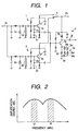
- Fig. 1 illustrates a structure of the two-band oscillating apparatus of the present invention, consisting of a first oscillator 1, a second oscillator 2 and an amplifier 3.
- the first oscillator 1 outputs an oscillation signal of the first frequency band (Lf) of the frequency as low as 880MHz to 940MHz
- the second oscillator 2 outputs an oscillation signal of the second frequency band (Hf) of 1805MHz to 1920MHz which is higher than the first frequency band.
- These oscillators are structured as the grounded-collector type voltage controlled oscillator.
- the first oscillator 1 is formed of a first oscillation transistor 1a, first feedback capacitors 1b, 1c, a first resonance line 1d and a first varactor diode 1e, etc., and the collector of the first oscillation transistor 1a is grounded in the high frequency manner through the first grounding capacitor 1f.
- the oscillation frequency of the first frequency band changes depending on the control voltage Vc impressed to the first varactor diode 1e and the oscillation signal can be extracted from the emitter.
- the second oscillator 2 is also formed of a second oscillation transistor 2a, second feedback capacitors 2b, 2c, a second resonance line 2d and a second varactor diode 2e, etc., and the collector of the second oscillation transistor 2a is grounded in the high frequency manner through the second grounding capacitor 2f.
- the oscillation frequency of the second frequency band changes depending on the control voltage Vc impressed to the second varactor diode 2e and the oscillation signal can be extracted from the emitter.
- the power source voltage (Vb) is applied, through the change-over switch 4, to any one of the collector of the first oscillation transistor 1a and the collector of the second oscillation transistor 2a, and the oscillator to which such power source voltage (Vb) is applied operates to output the oscillation signal.
- the amplifier 3 is formed as a grounded-emitter type amplifier in which the power source voltage is applied to the collector of the amplifying transistor 3a via the choke inductor 3b, and the emitter is grounded through a bias resistor 3c.
- the first series resonance means 3d and the second series resonance means 3e are connected in parallel between the emitter and ground.
- the first series resonance means 3d includes the serially connected first capacitance element 3d1 and the first inductance element 3d2 and is set to have the series resonance frequency almost in the first frequency band.
- the second series resonance means 3e includes the serially connected second capacitance element 3e1 and the second inductance element 3e2 and is set to have the series resonance frequency almost in the second frequency band.
- any type of means having the series resonance frequency in the first frequency band and the second frequency band can be used.
- the first capacitance element such as the first chip capacitor having the self series resonance frequency in the first frequency band may be used as the first series resonance means 3d
- the second capacitance element such as the second chip capacitor having the self series resonance frequency in the second frequency band may be used as the second series resonance means 3e.
- the first series resonance means 3d is formed of the first capacitance means having the same capacitance as that of the first capacitance element 3d1 and the first inductance means having the same inductance as that of the first inductance element 3d2
- the second series resonance means 3e is formed of the second capacitance means having the same capacitance as that of the second capacitance element 3e1 and the second inductance means having the same inductance as that of the second inductance element 3e2.
- the first inductance means is formed of a first conductor to connect the first capacitance means between the emitter of the amplifying transistor 3a and the ground
- the second inductance means is formed of a second conductor to connect the second capacitance means between the emitter of the amplifying transistor 3a and the ground.
- the amplification degree of the amplifier 3 is increased up to the almost equal level in the first and second frequency bands but is reduced in the other frequency bands as illustrated in Fig. 2.
- the first oscillator 1 When the power source voltage is applied to the collector of the first oscillation transistor 1a through the change-over switch 4, the first oscillator 1 operates to output the oscillation signal of the first frequency band and this output is then input to the amplifier 3. In this timing, since the power source voltage is not applied to the collector of the second oscillation transistor 2a, the second oscillator 2 does not operate.
- the oscillation signal in the first frequency band is amplified to a large extent by the amplifier 3 and it is output from the collector of the amplifying transistor 3a via the DC-cut capacitor 3f.
- the second oscillator 2 operates to output the oscillation signal of the second frequency band and this output signal is input to the amplifier 3.
- the first oscillator 1 since the power source voltage is not applied to the collector of the first oscillation transistor 1a, the first oscillator 1 does not operate.
- the oscillation signal of the second frequency band is then amplified to a large extent with the amplifier 3 and this amplified oscillation signal is output from the collector of the amplifying transistor 3a via the DC-cut capacitor 3f.
- the two-band oscillating apparatus of the present invention comprises the first oscillator for outputting an oscillation signal of the first frequency band, the second oscillator for outputting an oscillation signal of the second frequency band higher than the first frequency band and the grounded-emitter type amplifier for amplifying the oscillation signal of the first frequency band or second frequency band, wherein the bias resistor is connected between the emitter of amplifying transistor and the ground and the first series resonance means having the series resonance frequency in the first frequency band and the second series resonance means having the series resonance frequency in the second frequency band are also connected between the emitter and the ground, thereby the amplifier attains a large amplification degree in the first and second frequency bands with the simplified structure using a less number of parts and moreover the oscillation signals in the first and second frequency bands can be amplified almost up to the equal level.
- the two-band oscillating apparatus of the present invention utilizes the first capacitance element having the self series resonance frequency in the first frequency band as the first series resonance means and the second capacitance element having the self series resonance frequency in the second frequency band as the second series resonance means, the oscillation signal of the first frequency band and the oscillation signal of the second frequency band can be amplified almost up to the equal level only by utilizing the capacitance elements.
- the two-band oscillating apparatus of the present invention uses the first chip capacitor as the first capacitance element and the second chip capacitor as the second capacitance element and can therefore be reduced in size easily.
- the two-band oscillating apparatus of the present invention structures the first series resonance means with the first capacitance means and the first inductance means, and the second series resonance means with the second capacitance element and the second inductance means. Therefore, respective series resonance frequencies of the first series resonance means and the second series resonance means can be set easily.
- the two-band oscillating apparatus of the present invention comprises the first conductor for connecting the first capacitance means between the emitter and the ground and the second conductor for connecting the second capacitance means between the emitter and the ground, and uses the first conductor as the first inductance means and the second conductor as the second inductance means.
Landscapes
- Inductance-Capacitance Distribution Constants And Capacitance-Resistance Oscillators (AREA)
- Amplifiers (AREA)
Abstract
Description
- The present invention relates to a two-band oscillation apparatus to be used in a hand-held telephone set used in common for different two systems.
- Fig. 3 illustrates a structure of a two-band oscillation apparatus of the related art consisting of a
first oscillator 21, asecond oscillator 22 and anamplifier 23. Thefirst oscillator 21 is structured to oscillate at a low frequency band (Lf) of about 880 MHz to 940 MHz, while thesecond oscillator 22 is structured to oscillate at a high frequency band (Hf) of about 1805 MHz to 1920 MHz higher than the oscillation frequency of thefirst oscillator 21. - The power source voltage (Vb) is applied to the
first oscillator 21 orsecond oscillator 22 through a first change-overswitch 24 and the oscillator to which the power source voltage is applied operates to output an oscillation signal and anamplifier 23 amplifies such oscillation signal. - The
amplifier 23 is formed as an emitter-grounded tuning amplifier, wherein the power source voltage is impressed to the collector of the amplifyingtransistor 23a via achoke inductor 23b and the emitter of amplifying transistor is grounded through abias resistor 23c and abypass capacitor 23d. Moreover, a series circuit of atuning capacitor 23e and aswitching diode 23f is connected between the collector and ground. The cathode of switchingdiode 23f is grounded and a switching voltage (Vs) is impressed to the anode thereof via a second change-overswitch 25. The second change-overswitch 25 is changed over in conjunction with the first change-overswitch 24. - When the power source voltage is impressed to the
first oscillator 21 with the first change-overswitch 24, a switching voltage is impressed to the anode of theswitching diode 23f of theamplifier 23 via the second change-overswitch 25 to turn ON theswitching diode 23f. An oscillation signal of the low frequency band output from thefirst oscillator 21 is input to theamplifier 23. In theamplifier 23, a parallel tuning circuit is formed of achoke inductor 23b and atuning capacitor 23e when theswitching diode 23f turns ON. The tuning frequency is set almost to be matched with the low frequency band. Therefore, the amplifying characteristic of theamplifier 23 shows the peak amplification degree in the low frequency band as illustrated in A of Fig. 4. The oscillation signal of the low frequency band input to theamplifier 23 is amplified to a large extent and the amplified oscillation signal is output from the collector of amplifyingtransistor 23a via a DC-cut capacitor 23h. - On the other hand, when the power source voltage is impressed to the
second oscillator 22 with the first change-overswitch 24, a change-over voltage is no longer impressed to the anode of theswitching diode 23f ofamplifier 23 with the second change-overswitch 25 to turn OFF theswitching diode 23f. An oscillation signal of the high frequency band output from thesecond oscillator 22 is then input to theamplifier 23. In theamplifier 23, when theswitching diode 23f turns OFF, its terminal capacitance is connected in series to thetuning capacitor 23e and the combining capacitance of these elements is connected in parallel to thechoke inductor 23b to form a parallel tuning circuit. The tuning frequency is set almost to be matched with the high frequency band. Therefore, the amplifying characteristic of theamplifier 23 has the peak amplification degree in the high frequency band as illustrated in B of Fig. 4 and the oscillation signal of high frequency band input to theamplifier 23 is amplified to a large extent and the amplified oscillation signal is output from the collector of amplifyingtransistor 23a via the DC-cut capacitor 23h. - As explained above, the two-band oscillating apparatus of the related art forms an amplifier to amplify the oscillating signal of two frequency bands with a tuning amplifier and moreover the tuning frequency of the tuning circuit of the tuning amplifier is changed over. Therefore, a large number of parts are required to impede reduction in size of the circuit.
- Therefore, it is an object of the invention to provide a two-band oscillator which reduces the number of parts by simplifying the structure of amplifier and assures the higher amplification degree in two oscillation frequencies without changing-over of the amplifying characteristic.
- As a means for overcoming the problems explained above, the two-band oscillation apparatus of the present invention comprises a first oscillator for outputting the oscillation signal of the first frequency band, a second oscillator for outputting the oscillation signal of the second frequency band higher than the first frequency band and an emitter-grounded amplifier including an amplifying transistor to amplify the oscillation signal of the first frequency band or the oscillation signal of the second frequency band with the amplifying transistor, wherein a bias resistor is connected between the emitter of the amplifying transistor and the ground, moreover a first series resonance means having the series resonance frequency in the first frequency band and a second series resonance means having the series resonance frequency in the second frequency band are connected between the emitter and the ground.
- Preferably, the two-band oscillating apparatus uses a first capacitance element having the self series resonance frequency in the first frequency band as the first series resonance means and a second capacitance element having the self series resonance frequency in the second frequency band as the second series resonance means.
- Preferably, the two-band oscillating apparatus uses a first chip capacitor as the first capacitance element, while a second chip capacitor as the second capacitance element.
- Preferably, the two-band oscillating apparatus structures the first series resonance means with a first capacitance means and a first inductance means, and the second series resonance means with a second capacitance means and a second inductance means.
- In addition, the two-band oscillating apparatus. preferably also comprises a first conductor to connect the first capacitance means between the emitter and the ground and a second conductor to connect the second capacitance means between the emitter and the ground and defines the first conductor as the first inductance means and the second conductor as the second inductance means.
- Embodiments of the invention will now be described, by way of example only, with reference to the accompanying drawings, in which:
- Fig. 1 is a structural diagram of the two-band oscillating apparatus of the present invention.
- Fig. 2 is an amplifying characteristic diagram of an amplifier in the two-band oscillating apparatus of the present invention.
- Fig. 3 is a structural diagram of the two-band oscillating apparatus of the related art.
- Fig. 4 is an amplifying characteristic diagram of an amplifier in the two-band oscillating apparatus of the related art.
-
- Fig. 1 illustrates a structure of the two-band oscillating apparatus of the present invention, consisting of a first oscillator 1, a second oscillator 2 and an
amplifier 3. The first oscillator 1 outputs an oscillation signal of the first frequency band (Lf) of the frequency as low as 880MHz to 940MHz, while the second oscillator 2 outputs an oscillation signal of the second frequency band (Hf) of 1805MHz to 1920MHz which is higher than the first frequency band. These oscillators are structured as the grounded-collector type voltage controlled oscillator. - That is, the first oscillator 1 is formed of a
first oscillation transistor 1a,first feedback capacitors first resonance line 1d and afirst varactor diode 1e, etc., and the collector of thefirst oscillation transistor 1a is grounded in the high frequency manner through thefirst grounding capacitor 1f. The oscillation frequency of the first frequency band changes depending on the control voltage Vc impressed to thefirst varactor diode 1e and the oscillation signal can be extracted from the emitter. - The second oscillator 2 is also formed of a
second oscillation transistor 2a,second feedback capacitors second resonance line 2d and a second varactor diode 2e, etc., and the collector of thesecond oscillation transistor 2a is grounded in the high frequency manner through the second grounding capacitor 2f. The oscillation frequency of the second frequency band changes depending on the control voltage Vc impressed to the second varactor diode 2e and the oscillation signal can be extracted from the emitter. - The power source voltage (Vb) is applied, through the change-over switch 4, to any one of the collector of the
first oscillation transistor 1a and the collector of thesecond oscillation transistor 2a, and the oscillator to which such power source voltage (Vb) is applied operates to output the oscillation signal. Theamplifier 3 is formed as a grounded-emitter type amplifier in which the power source voltage is applied to the collector of the amplifyingtransistor 3a via thechoke inductor 3b, and the emitter is grounded through a bias resistor 3c. Moreover, the first series resonance means 3d and the second series resonance means 3e are connected in parallel between the emitter and ground. - The first series resonance means 3d includes the serially connected first capacitance element 3d1 and the first inductance element 3d2 and is set to have the series resonance frequency almost in the first frequency band. In the same manner, the second series resonance means 3e includes the serially connected second capacitance element 3e1 and the second inductance element 3e2 and is set to have the series resonance frequency almost in the second frequency band.
- As the first series resonance means 3d and second series resonance means 3e, any type of means having the series resonance frequency in the first frequency band and the second frequency band can be used. For instance, since a so-called chip capacitor which is a leadless type capacitance element has the self series resonance frequency from its structural viewpoint, the first capacitance element such as the first chip capacitor having the self series resonance frequency in the first frequency band may be used as the first series resonance means 3d, while the second capacitance element such as the second chip capacitor having the self series resonance frequency in the second frequency band may be used as the second series resonance means 3e.
- Moreover, it is also possible that the first series resonance means 3d is formed of the first capacitance means having the same capacitance as that of the first capacitance element 3d1 and the first inductance means having the same inductance as that of the first inductance element 3d2, while the second series resonance means 3e is formed of the second capacitance means having the same capacitance as that of the second capacitance element 3e1 and the second inductance means having the same inductance as that of the second inductance element 3e2.
- Moreover, it is also possible that the first inductance means is formed of a first conductor to connect the first capacitance means between the emitter of the amplifying
transistor 3a and the ground, while the second inductance means is formed of a second conductor to connect the second capacitance means between the emitter of the amplifyingtransistor 3a and the ground. - As explained above, since the negative feedback is not effective in the first and second frequency bands for the emitter of the amplifying
transistor 3a but is effective in the other frequency bands by using the first series resonance means 3d and second series resonance means 3e, the amplification degree of theamplifier 3 is increased up to the almost equal level in the first and second frequency bands but is reduced in the other frequency bands as illustrated in Fig. 2. - When the power source voltage is applied to the collector of the
first oscillation transistor 1a through the change-over switch 4, the first oscillator 1 operates to output the oscillation signal of the first frequency band and this output is then input to theamplifier 3. In this timing, since the power source voltage is not applied to the collector of thesecond oscillation transistor 2a, the second oscillator 2 does not operate. The oscillation signal in the first frequency band is amplified to a large extent by theamplifier 3 and it is output from the collector of the amplifyingtransistor 3a via the DC-cut capacitor 3f. - Meanwhile, when the power source voltage is applied to the collector of the
second oscillation transistor 2a through the change-over switch 4, the second oscillator 2 operates to output the oscillation signal of the second frequency band and this output signal is input to theamplifier 3. In this timing, since the power source voltage is not applied to the collector of thefirst oscillation transistor 1a, the first oscillator 1 does not operate. The oscillation signal of the second frequency band is then amplified to a large extent with theamplifier 3 and this amplified oscillation signal is output from the collector of the amplifyingtransistor 3a via the DC-cut capacitor 3f. - As explained above, the two-band oscillating apparatus of the present invention comprises the first oscillator for outputting an oscillation signal of the first frequency band, the second oscillator for outputting an oscillation signal of the second frequency band higher than the first frequency band and the grounded-emitter type amplifier for amplifying the oscillation signal of the first frequency band or second frequency band, wherein the bias resistor is connected between the emitter of amplifying transistor and the ground and the first series resonance means having the series resonance frequency in the first frequency band and the second series resonance means having the series resonance frequency in the second frequency band are also connected between the emitter and the ground, thereby the amplifier attains a large amplification degree in the first and second frequency bands with the simplified structure using a less number of parts and moreover the oscillation signals in the first and second frequency bands can be amplified almost up to the equal level.
- In addition, since the two-band oscillating apparatus of the present invention utilizes the first capacitance element having the self series resonance frequency in the first frequency band as the first series resonance means and the second capacitance element having the self series resonance frequency in the second frequency band as the second series resonance means, the oscillation signal of the first frequency band and the oscillation signal of the second frequency band can be amplified almost up to the equal level only by utilizing the capacitance elements.
- Moreover, the two-band oscillating apparatus of the present invention uses the first chip capacitor as the first capacitance element and the second chip capacitor as the second capacitance element and can therefore be reduced in size easily.
- Moreover, the two-band oscillating apparatus of the present invention structures the first series resonance means with the first capacitance means and the first inductance means, and the second series resonance means with the second capacitance element and the second inductance means. Therefore, respective series resonance frequencies of the first series resonance means and the second series resonance means can be set easily.
- Moreover, the two-band oscillating apparatus of the present invention comprises the first conductor for connecting the first capacitance means between the emitter and the ground and the second conductor for connecting the second capacitance means between the emitter and the ground, and uses the first conductor as the first inductance means and the second conductor as the second inductance means. Thereby, the number of parts can be reduced.
Claims (5)
- A two-band oscillating apparatus comprising: a first oscillator for outputting an oscillation signal of the first frequency band; a second oscillator for outputting an oscillation signal of the second frequency band which is higher than the first frequency band; and a grounded-emitter type amplifier including an amplifying transistor and amplifying the oscillation signal of first frequency band and oscillation signal of second frequency band with the amplifying transistor, wherein a bias resistor is connected between the emitter of the amplifying transistor and the ground and both first series resonance means having the series resonance frequency in the first frequency band and second series resonance means having the series resonance frequency in the second frequency band are connected between the emitter and the ground.
- A two-band oscillating apparatus according to claim 1, wherein a first capacitance element having the self series resonance frequency in the first frequency band is used as the first series resonance means, while a second capacitance element having the self series resonance frequency in the second frequency band is used as the second series resonance means.
- A two-band oscillating apparatus according to claim 2, wherein the first capacitance element is used as a first chip capacitor, while the second capacitance element as a second chip capacitor.
- A two-band oscillating apparatus according to claim 1, wherein the first series resonance means is structured with the first capacitance means and the first inductance means, while the second series resonance means is structured with the second capacitance means and the second inductance means.
- A two-band oscillating apparatus according to claim 4, wherein a first conductor is provided to connect the first capacitance means between the emitter and ground, a second conductor is provided to connect the second capacitance means between the emitter and ground, and the first conductor is used as the first inductance means, while the second conductor as the second inductance means.
Applications Claiming Priority (2)
| Application Number | Priority Date | Filing Date | Title |
|---|---|---|---|
| JP11232598A JP2001060826A (en) | 1999-08-19 | 1999-08-19 | Two-band oscillating device |
| JP23259899 | 1999-08-19 |
Publications (2)
| Publication Number | Publication Date |
|---|---|
| EP1079513A1 true EP1079513A1 (en) | 2001-02-28 |
| EP1079513B1 EP1079513B1 (en) | 2003-10-29 |
Family
ID=16941880
Family Applications (1)
| Application Number | Title | Priority Date | Filing Date |
|---|---|---|---|
| EP00306530A Expired - Lifetime EP1079513B1 (en) | 1999-08-19 | 2000-07-31 | Oscillating apparatus including two-band resonance circuit |
Country Status (4)
| Country | Link |
|---|---|
| US (1) | US6292063B1 (en) |
| EP (1) | EP1079513B1 (en) |
| JP (1) | JP2001060826A (en) |
| DE (1) | DE60006197T2 (en) |
Cited By (1)
| Publication number | Priority date | Publication date | Assignee | Title |
|---|---|---|---|---|
| EP1239601A3 (en) * | 2001-03-06 | 2003-06-25 | Alps Electric Co., Ltd. | Dual-Band oscillator for preventing reduction in oscillation power caused by bias resistor |
Families Citing this family (7)
| Publication number | Priority date | Publication date | Assignee | Title |
|---|---|---|---|---|
| JP2001237640A (en) * | 2000-02-21 | 2001-08-31 | Murata Mfg Co Ltd | Voltage controlled oscillator and communication equipment |
| KR20030053791A (en) * | 2001-12-24 | 2003-07-02 | 삼성전기주식회사 | Voltage-controlled oscillation circuit with function of simple operation select |
| JP2006238034A (en) * | 2005-02-24 | 2006-09-07 | Alps Electric Co Ltd | Oscillation circuit |
| KR100990013B1 (en) * | 2006-03-16 | 2010-10-26 | 가부시키가이샤 무라타 세이사쿠쇼 | High frequency oscillators and electronics |
| US8193868B2 (en) * | 2010-04-28 | 2012-06-05 | Freescale Semiconductor, Inc. | Switched capacitor circuit for a voltage controlled oscillator |
| US8264295B2 (en) | 2010-08-31 | 2012-09-11 | Freescale Semiconductor, Inc. | Switched varactor circuit for a voltage controlled oscillator |
| JP6178087B2 (en) * | 2013-03-14 | 2017-08-09 | 浜松ホトニクス株式会社 | Flash light source device |
Citations (2)
| Publication number | Priority date | Publication date | Assignee | Title |
|---|---|---|---|---|
| GB1002941A (en) * | 1963-05-20 | 1965-09-02 | Gen Electric Co Ltd | Improvements in or relating to electric filter networks |
| EP0886384A2 (en) * | 1997-06-13 | 1998-12-23 | Lucent Technologies Inc. | Single-stage dual-band low-noise amplifier for use in a wireless communication system receiver |
Family Cites Families (4)
| Publication number | Priority date | Publication date | Assignee | Title |
|---|---|---|---|---|
| US5852384A (en) * | 1996-04-25 | 1998-12-22 | Matsushita Electric Industrial Co., Ltd. | Dual band oscillator circuit using strip line resonators |
| JPH09294018A (en) | 1996-04-25 | 1997-11-11 | Matsushita Electric Ind Co Ltd | High frequency dual band oscillator |
| JPH10163750A (en) * | 1996-11-27 | 1998-06-19 | Tdk Corp | Voltage control oscillator |
| JP3648979B2 (en) | 1998-04-07 | 2005-05-18 | 松下電器産業株式会社 | Oscillator and high-frequency module using the same |
-
1999
- 1999-08-19 JP JP11232598A patent/JP2001060826A/en active Pending
-
2000
- 2000-07-31 DE DE60006197T patent/DE60006197T2/en not_active Expired - Fee Related
- 2000-07-31 EP EP00306530A patent/EP1079513B1/en not_active Expired - Lifetime
- 2000-08-08 US US09/634,516 patent/US6292063B1/en not_active Expired - Fee Related
Patent Citations (2)
| Publication number | Priority date | Publication date | Assignee | Title |
|---|---|---|---|---|
| GB1002941A (en) * | 1963-05-20 | 1965-09-02 | Gen Electric Co Ltd | Improvements in or relating to electric filter networks |
| EP0886384A2 (en) * | 1997-06-13 | 1998-12-23 | Lucent Technologies Inc. | Single-stage dual-band low-noise amplifier for use in a wireless communication system receiver |
Cited By (2)
| Publication number | Priority date | Publication date | Assignee | Title |
|---|---|---|---|---|
| EP1239601A3 (en) * | 2001-03-06 | 2003-06-25 | Alps Electric Co., Ltd. | Dual-Band oscillator for preventing reduction in oscillation power caused by bias resistor |
| KR100468808B1 (en) * | 2001-03-06 | 2005-01-29 | 알프스 덴키 가부시키가이샤 | Two-band oscillator |
Also Published As
| Publication number | Publication date |
|---|---|
| EP1079513B1 (en) | 2003-10-29 |
| JP2001060826A (en) | 2001-03-06 |
| US6292063B1 (en) | 2001-09-18 |
| DE60006197D1 (en) | 2003-12-04 |
| DE60006197T2 (en) | 2004-06-09 |
Similar Documents
| Publication | Publication Date | Title |
|---|---|---|
| EP0803972B1 (en) | Dual band oscillator circuit | |
| EP0893878B1 (en) | High frequency oscillating circuit | |
| KR100457939B1 (en) | High frequency crystal oscillator | |
| KR960003560B1 (en) | Voltage controlled oscillation circuit | |
| EP1079513B1 (en) | Oscillating apparatus including two-band resonance circuit | |
| KR100260965B1 (en) | Amplifier and portable telephone apparatus using the same | |
| US6163222A (en) | Buffer amplifier with frequency selective mechanism | |
| JPH09294018A (en) | High frequency dual band oscillator | |
| JPH07106851A (en) | Oscillation circuit | |
| US6593822B2 (en) | Oscillator for achieving stable oscillation | |
| US6724274B2 (en) | Frequency-switching oscillator and electronic device using the same | |
| KR100389106B1 (en) | Oscillator | |
| JPH09307354A (en) | Resonator and voltage controlled oscillator using the same | |
| EP1154559B1 (en) | Oscillator | |
| EP1081846B1 (en) | Voltage controled oscillator | |
| JP4332339B2 (en) | 2-band oscillator | |
| JP3318504B2 (en) | Voltage controlled high frequency oscillator | |
| JPH104315A (en) | High frequency oscillation circuit | |
| JP2000332535A (en) | Frequency band switching type voltage-controlled oscillator | |
| JPH03204205A (en) | Integrated circuit device | |
| JP2005039596A (en) | Integrated oscillator circuit | |
| JP3955460B2 (en) | 2-band oscillator | |
| JPS6017933Y2 (en) | Base grounded transistor amplifier circuit | |
| US6522211B1 (en) | Frequency-switching oscillator and communication apparatus using same | |
| JPH09162641A (en) | Voltage control oscillator |
Legal Events
| Date | Code | Title | Description |
|---|---|---|---|
| PUAI | Public reference made under article 153(3) epc to a published international application that has entered the european phase |
Free format text: ORIGINAL CODE: 0009012 |
|
| 17P | Request for examination filed |
Effective date: 20001123 |
|
| AK | Designated contracting states |
Kind code of ref document: A1 Designated state(s): AT BE CH CY DE DK ES FI FR GB GR IE IT LI LU MC NL PT SE |
|
| AX | Request for extension of the european patent |
Free format text: AL;LT;LV;MK;RO;SI |
|
| AKX | Designation fees paid |
Free format text: DE FR |
|
| GRAH | Despatch of communication of intention to grant a patent |
Free format text: ORIGINAL CODE: EPIDOS IGRA |
|
| GRAS | Grant fee paid |
Free format text: ORIGINAL CODE: EPIDOSNIGR3 |
|
| GRAA | (expected) grant |
Free format text: ORIGINAL CODE: 0009210 |
|
| AK | Designated contracting states |
Kind code of ref document: B1 Designated state(s): DE FR |
|
| REF | Corresponds to: |
Ref document number: 60006197 Country of ref document: DE Date of ref document: 20031204 Kind code of ref document: P |
|
| ET | Fr: translation filed | ||
| PLBE | No opposition filed within time limit |
Free format text: ORIGINAL CODE: 0009261 |
|
| STAA | Information on the status of an ep patent application or granted ep patent |
Free format text: STATUS: NO OPPOSITION FILED WITHIN TIME LIMIT |
|
| 26N | No opposition filed |
Effective date: 20040730 |
|
| PGFP | Annual fee paid to national office [announced via postgrant information from national office to epo] |
Ref country code: FR Payment date: 20050719 Year of fee payment: 6 |
|
| PGFP | Annual fee paid to national office [announced via postgrant information from national office to epo] |
Ref country code: DE Payment date: 20050926 Year of fee payment: 6 |
|
| PG25 | Lapsed in a contracting state [announced via postgrant information from national office to epo] |
Ref country code: DE Free format text: LAPSE BECAUSE OF NON-PAYMENT OF DUE FEES Effective date: 20070201 |
|
| REG | Reference to a national code |
Ref country code: FR Ref legal event code: ST Effective date: 20070330 |
|
| PG25 | Lapsed in a contracting state [announced via postgrant information from national office to epo] |
Ref country code: FR Free format text: LAPSE BECAUSE OF NON-PAYMENT OF DUE FEES Effective date: 20060731 |