EP1079411B1 - Electrophotographic screening method with humidity and temperature insensitive organic conductor - Google Patents
Electrophotographic screening method with humidity and temperature insensitive organic conductor Download PDFInfo
- Publication number
- EP1079411B1 EP1079411B1 EP00402313A EP00402313A EP1079411B1 EP 1079411 B1 EP1079411 B1 EP 1079411B1 EP 00402313 A EP00402313 A EP 00402313A EP 00402313 A EP00402313 A EP 00402313A EP 1079411 B1 EP1079411 B1 EP 1079411B1
- Authority
- EP
- European Patent Office
- Prior art keywords
- layer
- pedt
- pss
- poly
- solution
- Prior art date
- Legal status (The legal status is an assumption and is not a legal conclusion. Google has not performed a legal analysis and makes no representation as to the accuracy of the status listed.)
- Expired - Lifetime
Links
- 238000000034 method Methods 0.000 title claims description 14
- 239000004020 conductor Substances 0.000 title description 3
- 238000012216 screening Methods 0.000 title description 3
- 229920001609 Poly(3,4-ethylenedioxythiophene) Polymers 0.000 claims description 51
- 229920002338 polyhydroxyethylmethacrylate Polymers 0.000 claims description 21
- WOBHKFSMXKNTIM-UHFFFAOYSA-N Hydroxyethyl methacrylate Chemical compound CC(=C)C(=O)OCCO WOBHKFSMXKNTIM-UHFFFAOYSA-N 0.000 claims description 16
- 229920000036 polyvinylpyrrolidone Polymers 0.000 claims description 16
- 235000013855 polyvinylpyrrolidone Nutrition 0.000 claims description 16
- 239000001267 polyvinylpyrrolidone Substances 0.000 claims description 16
- 229920002845 Poly(methacrylic acid) Polymers 0.000 claims description 15
- 239000000463 material Substances 0.000 claims description 11
- 229920002037 poly(vinyl butyral) polymer Polymers 0.000 claims description 10
- 229920000642 polymer Polymers 0.000 claims description 10
- 239000004793 Polystyrene Substances 0.000 claims description 9
- 229920002223 polystyrene Polymers 0.000 claims description 9
- 239000002904 solvent Substances 0.000 claims description 7
- 239000011248 coating agent Substances 0.000 claims description 6
- 238000000576 coating method Methods 0.000 claims description 6
- 229920001577 copolymer Polymers 0.000 claims description 6
- JXLHNMVSKXFWAO-UHFFFAOYSA-N azane;7-fluoro-2,1,3-benzoxadiazole-4-sulfonic acid Chemical compound N.OS(=O)(=O)C1=CC=C(F)C2=NON=C12 JXLHNMVSKXFWAO-UHFFFAOYSA-N 0.000 claims description 5
- 239000004094 surface-active agent Substances 0.000 claims description 5
- 125000000391 vinyl group Chemical group [H]C([*])=C([H])[H] 0.000 claims description 5
- 229920002554 vinyl polymer Polymers 0.000 claims description 5
- XLYOFNOQVPJJNP-UHFFFAOYSA-N water Chemical compound O XLYOFNOQVPJJNP-UHFFFAOYSA-N 0.000 claims description 5
- 238000004519 manufacturing process Methods 0.000 claims description 4
- 239000000470 constituent Substances 0.000 claims description 2
- 238000006073 displacement reaction Methods 0.000 claims description 2
- 230000005855 radiation Effects 0.000 claims description 2
- 238000005269 aluminizing Methods 0.000 claims 1
- 239000002518 antifoaming agent Substances 0.000 claims 1
- 239000008367 deionised water Substances 0.000 claims 1
- 229910021641 deionized water Inorganic materials 0.000 claims 1
- 239000000243 solution Substances 0.000 description 24
- OKKJLVBELUTLKV-UHFFFAOYSA-N Methanol Chemical compound OC OKKJLVBELUTLKV-UHFFFAOYSA-N 0.000 description 21
- WIJWBOWLVOOYFR-BDSSXFGHSA-N (9R,13R)-1a,1b-dinor-10,11-dihydro-12-oxo-15-phytoenoic acid Chemical compound CC\C=C/C[C@@H]1[C@H](CCCCCC(O)=O)CCC1=O WIJWBOWLVOOYFR-BDSSXFGHSA-N 0.000 description 11
- 238000003756 stirring Methods 0.000 description 10
- OAICVXFJPJFONN-UHFFFAOYSA-N Phosphorus Chemical compound [P] OAICVXFJPJFONN-UHFFFAOYSA-N 0.000 description 9
- 239000011159 matrix material Substances 0.000 description 9
- 229920002120 photoresistant polymer Polymers 0.000 description 8
- 239000011550 stock solution Substances 0.000 description 7
- 239000008199 coating composition Substances 0.000 description 6
- 239000011521 glass Substances 0.000 description 5
- 239000000203 mixture Substances 0.000 description 5
- SJEBAWHUJDUKQK-UHFFFAOYSA-N 2-ethylanthraquinone Chemical compound C1=CC=C2C(=O)C3=CC(CC)=CC=C3C(=O)C2=C1 SJEBAWHUJDUKQK-UHFFFAOYSA-N 0.000 description 4
- CTQNGGLPUBDAKN-UHFFFAOYSA-N O-Xylene Chemical compound CC1=CC=CC=C1C CTQNGGLPUBDAKN-UHFFFAOYSA-N 0.000 description 4
- 238000010894 electron beam technology Methods 0.000 description 4
- 108091008695 photoreceptors Proteins 0.000 description 4
- 239000008096 xylene Substances 0.000 description 4
- MQIUGAXCHLFZKX-UHFFFAOYSA-N Di-n-octyl phthalate Natural products CCCCCCCCOC(=O)C1=CC=CC=C1C(=O)OCCCCCCCC MQIUGAXCHLFZKX-UHFFFAOYSA-N 0.000 description 3
- YXFVVABEGXRONW-UHFFFAOYSA-N Toluene Chemical compound CC1=CC=CC=C1 YXFVVABEGXRONW-UHFFFAOYSA-N 0.000 description 3
- 239000011358 absorbing material Substances 0.000 description 3
- BJQHLKABXJIVAM-UHFFFAOYSA-N bis(2-ethylhexyl) phthalate Chemical compound CCCCC(CC)COC(=O)C1=CC=CC=C1C(=O)OCC(CC)CCCC BJQHLKABXJIVAM-UHFFFAOYSA-N 0.000 description 3
- 230000007423 decrease Effects 0.000 description 3
- 239000007787 solid Substances 0.000 description 3
- CSCPPACGZOOCGX-UHFFFAOYSA-N Acetone Chemical compound CC(C)=O CSCPPACGZOOCGX-UHFFFAOYSA-N 0.000 description 2
- KRHYYFGTRYWZRS-UHFFFAOYSA-N Fluorane Chemical compound F KRHYYFGTRYWZRS-UHFFFAOYSA-N 0.000 description 2
- PPBRXRYQALVLMV-UHFFFAOYSA-N Styrene Chemical compound C=CC1=CC=CC=C1 PPBRXRYQALVLMV-UHFFFAOYSA-N 0.000 description 2
- 239000000654 additive Substances 0.000 description 2
- 229910052782 aluminium Inorganic materials 0.000 description 2
- XAGFODPZIPBFFR-UHFFFAOYSA-N aluminium Chemical compound [Al] XAGFODPZIPBFFR-UHFFFAOYSA-N 0.000 description 2
- 239000004615 ingredient Substances 0.000 description 2
- 239000010416 ion conductor Substances 0.000 description 2
- 238000005259 measurement Methods 0.000 description 2
- 229920000620 organic polymer Polymers 0.000 description 2
- 229920003023 plastic Polymers 0.000 description 2
- 239000004033 plastic Substances 0.000 description 2
- 230000000717 retained effect Effects 0.000 description 2
- 238000004528 spin coating Methods 0.000 description 2
- 238000002411 thermogravimetry Methods 0.000 description 2
- 229910052724 xenon Inorganic materials 0.000 description 2
- FHNFHKCVQCLJFQ-UHFFFAOYSA-N xenon atom Chemical compound [Xe] FHNFHKCVQCLJFQ-UHFFFAOYSA-N 0.000 description 2
- VHQGURIJMFPBKS-UHFFFAOYSA-N 2,4,7-trinitrofluoren-9-one Chemical compound [O-][N+](=O)C1=CC([N+]([O-])=O)=C2C3=CC=C([N+](=O)[O-])C=C3C(=O)C2=C1 VHQGURIJMFPBKS-UHFFFAOYSA-N 0.000 description 1
- JMPRVUAYOASENX-UHFFFAOYSA-N 4-phenylbuta-1,2,3-trienylbenzene Chemical compound C=1C=CC=CC=1C=C=C=CC1=CC=CC=C1 JMPRVUAYOASENX-UHFFFAOYSA-N 0.000 description 1
- 229920002035 Pluronic® L 10 Polymers 0.000 description 1
- 229920002359 Tetronic® Polymers 0.000 description 1
- 239000004480 active ingredient Substances 0.000 description 1
- 230000000996 additive effect Effects 0.000 description 1
- 239000007864 aqueous solution Substances 0.000 description 1
- 239000003518 caustics Substances 0.000 description 1
- 125000004122 cyclic group Chemical group 0.000 description 1
- 230000001419 dependent effect Effects 0.000 description 1
- 238000010586 diagram Methods 0.000 description 1
- 238000010790 dilution Methods 0.000 description 1
- 239000012895 dilution Substances 0.000 description 1
- 239000000839 emulsion Substances 0.000 description 1
- 238000005530 etching Methods 0.000 description 1
- 238000001704 evaporation Methods 0.000 description 1
- 230000008020 evaporation Effects 0.000 description 1
- 230000003993 interaction Effects 0.000 description 1
- 230000001788 irregular Effects 0.000 description 1
- QSHDDOUJBYECFT-UHFFFAOYSA-N mercury Chemical compound [Hg] QSHDDOUJBYECFT-UHFFFAOYSA-N 0.000 description 1
- 229910052753 mercury Inorganic materials 0.000 description 1
- 229910052751 metal Inorganic materials 0.000 description 1
- 239000002184 metal Substances 0.000 description 1
- 239000011368 organic material Substances 0.000 description 1
- 239000003960 organic solvent Substances 0.000 description 1
- 230000002093 peripheral effect Effects 0.000 description 1
- 238000011045 prefiltration Methods 0.000 description 1
- 229920005989 resin Polymers 0.000 description 1
- 239000011347 resin Substances 0.000 description 1
- 239000007921 spray Substances 0.000 description 1
- 229910001220 stainless steel Inorganic materials 0.000 description 1
- 239000010935 stainless steel Substances 0.000 description 1
- JLZUZNKTTIRERF-UHFFFAOYSA-N tetraphenylethylene Chemical compound C1=CC=CC=C1C(C=1C=CC=CC=1)=C(C=1C=CC=CC=1)C1=CC=CC=C1 JLZUZNKTTIRERF-UHFFFAOYSA-N 0.000 description 1
- 238000005979 thermal decomposition reaction Methods 0.000 description 1
- 230000008719 thickening Effects 0.000 description 1
- FHYUCVWDMABHHH-UHFFFAOYSA-N toluene;1,2-xylene Chemical compound CC1=CC=CC=C1.CC1=CC=CC=C1C FHYUCVWDMABHHH-UHFFFAOYSA-N 0.000 description 1
- 239000004034 viscosity adjusting agent Substances 0.000 description 1
- 238000005406 washing Methods 0.000 description 1
Images


Classifications
-
- G—PHYSICS
- G03—PHOTOGRAPHY; CINEMATOGRAPHY; ANALOGOUS TECHNIQUES USING WAVES OTHER THAN OPTICAL WAVES; ELECTROGRAPHY; HOLOGRAPHY
- G03C—PHOTOSENSITIVE MATERIALS FOR PHOTOGRAPHIC PURPOSES; PHOTOGRAPHIC PROCESSES, e.g. CINE, X-RAY, COLOUR, STEREO-PHOTOGRAPHIC PROCESSES; AUXILIARY PROCESSES IN PHOTOGRAPHY
- G03C5/00—Photographic processes or agents therefor; Regeneration of such processing agents
-
- H—ELECTRICITY
- H01—ELECTRIC ELEMENTS
- H01J—ELECTRIC DISCHARGE TUBES OR DISCHARGE LAMPS
- H01J9/00—Apparatus or processes specially adapted for the manufacture, installation, removal, maintenance of electric discharge tubes, discharge lamps, or parts thereof; Recovery of material from discharge tubes or lamps
- H01J9/20—Manufacture of screens on or from which an image or pattern is formed, picked up, converted or stored; Applying coatings to the vessel
- H01J9/22—Applying luminescent coatings
- H01J9/221—Applying luminescent coatings in continuous layers
- H01J9/225—Applying luminescent coatings in continuous layers by electrostatic or electrophoretic processes
-
- H—ELECTRICITY
- H01—ELECTRIC ELEMENTS
- H01J—ELECTRIC DISCHARGE TUBES OR DISCHARGE LAMPS
- H01J9/00—Apparatus or processes specially adapted for the manufacture, installation, removal, maintenance of electric discharge tubes, discharge lamps, or parts thereof; Recovery of material from discharge tubes or lamps
- H01J9/20—Manufacture of screens on or from which an image or pattern is formed, picked up, converted or stored; Applying coatings to the vessel
- H01J9/22—Applying luminescent coatings
- H01J9/227—Applying luminescent coatings with luminescent material discontinuously arranged, e.g. in dots or lines
- H01J9/2276—Development of latent electrostatic images
Definitions
- the invention relates to a method of electrophotographically manufacturing a luminescent screen assembly for a cathode-ray tube (CRT) and, more particularly, to a method in which improved materials are used to provide an organic conductive (OC) layer which acts as an electrode for an overlying organic photoconductive (OPC) layer.
- OPC organic photoconductive
- the improved organic conductive (OC) layer has superior physical and electrical properties compared to prior organic conductive (OC) layers.
- a method of electrophotographically manufacturing a luminescent screen assembly on an interior surface of a faceplate panel of a color CRT includes the steps of coating the surface of the panel with a conductive solution to form a volatilizable organic conductive layer, and overcoating the organic conductive layer with a photoconductive solution to form a volatilizable photoconductive layer.
- the conductive solution comprises the organic polymer 3,4-polyethylene dioxythiophene polystyrene sulphonate (PEDT/PSS); a polymer or co-polymer to reduce organic residue selected from the group consisting of polyvinylpyrrolidone (PVP), poly (vinyl pyridine-co-vinyl acetate) (PVPy-VAc), polymethacrylic acid (PMAA), poly (hydroxyethylacrylate-co-methacrylic acid) (PHEA-MAA), poly (2-hydroxyethyl methacrylate) (PHEMA), and polyvinylbutyral (PVB); and a suitable solvent.
- PVP polyvinylpyrrolidone
- PMAA poly (vinyl pyridine-co-vinyl acetate)
- PMAA polymethacrylic acid
- PHEA-MAA poly (hydroxyethylacrylate-co-methacrylic acid)
- PHEMA poly (2-hydroxyethyl
- Fig. 1 shows a color CRT 10 having a glass envelope 11 comprising a rectangular faceplate panel 12 and a tubular neck 14 connected by a rectangular funnel 15.
- the funnel 15 has an internal conductive coating (not shown) that contacts an anode button 16 and extends into the neck 14.
- the panel 12 comprises a viewing faceplate 17 and a peripheral flange or sidewall 18, which is sealed to the funnel 15 by a glass frit 19.
- a relatively thin, light absorbing matrix 20, having a plurality of openings 21, is provided on an interior surface of the viewing faceplate 17.
- a luminescent three color phosphor screen 22 is carried on the interior surface of the faceplate 17 and overlies the matrix 20.
- the screen 22 preferably, is a line screen which includes a multiplicity of screen elements comprised of red-, blue-, and green-emitting phosphor stripes, R, B, and G, centered in different ones of the matrix openings and arranged in color groups or picture elements of three stripes or triads, in a cyclic order.
- the stripes extend in a direction that is generally normal to the plane in which the electron beams are generated. In the normal viewing position of the embodiment, the phosphor stripes extend in the vertical direction. Preferably, portions of the phosphor stripes overlap at least a portion of the light absorptive matrix 20 surrounding the openings 21. Alternatively, a dot screen may be utilized.
- the screen 22 and the overlying aluminum layer 24 comprise a screen assembly.
- a multi-apertured color selection electrode, such as a shadow mask or focus mask, 25 is removably mounted, by conventional means, in predetermined spaced relation to the screen assembly.
- An electron gun 27, shown schematically by the dashed lines in Fig. 1, is centrally mounted within the neck 14, to generate and direct three electron beams 28 along convergent paths, through the apertures in the color selection electrode 25, to the screen 22.
- the electron gun is conventional and may be any suitable gun known in the art.
- the tube 10 is designed to be used with an external magnetic deflection yoke, such as yoke 30, located in the region of the funnel-to-neck junction.
- an external magnetic deflection yoke such as yoke 30, located in the region of the funnel-to-neck junction.
- the yoke 30 subjects the three beams 28 to magnetic fields that cause the beams to scan horizontally and vertically, in a rectangular raster, over the screen 22.
- the initial plane of deflection (at zero deflection) is shown by the line P - P in Fig. 1, at about the middle of the yoke 30.
- the actual curvatures of the deflection beam paths, in the deflection zone are not shown.
- the screen 22 is manufactured by an electrophotographic screening (EPS) process that is described in U.S. Pat. No. 4,921,767, issued to Datta et al. on May 1, 1990.
- EPS electrophotographic screening
- step 31 the panel 12 is cleaned by washing it with a caustic solution, rinsing it in water, etching it with buffered hydrofluoric acid and rinsing it again with water, as is known in the art.
- the interior surface of the viewing faceplate 17 is provided with the light absorbing matrix 20, preferably, using the conventional wet matrix process described in U.S. Pat. No. 3,558,310, issued to Mayaud on Jan. 26, 1971.
- a suitable photoresist solution is applied to the interior surface, e.g., by spin coating, and the solution is dried to form a photoresist layer.
- the color selection electrode 25 is inserted into the panel 12 and the panel is placed onto a three-in-one lighthouse (not shown) which exposes the photoresist layer to actinic radiation from a light source which projects light through the openings in the color selection electrode.
- the exposure is repeated two more times with the light source located to simulate the paths of the electron beams from the three electron guns. The light selectively alters the solubility of the exposed areas of the photoresist layer.
- the panel is removed from the lighthouse and the color selection electrode is removed from the panel.
- the photoresist layer is developed, using water, to remove the more soluble areas thereof, thereby exposing the underlying interior surface of the viewing faceplate, and leaving the less soluble, exposed areas of the photoresist layer intact. Then, a suitable solution of light-absorbing material is uniformly provided onto the interior surface of the faceplate panel to cover the exposed portion of the viewing faceplate and the retained, less soluble, areas of the photoresist layer. The layer of light-absorbing material is dried and developed using a suitable solution which will dissolve and remove the retained portion of the photoresist layer and the overlying light-absorbing material, forming the openings 21 in the matrix 20 which is adhered to the interior surface of the viewing faceplate.
- a novel conductive solution as indicated in step 35 to form a layer 32 of a volatilizable, organic conductive (OC) material, shown in Fig. 4.
- OC organic conductive
- step 37 and shown in Fig. 4 the OC layer 32 provides an electrode for an overlying volatilizable, organic photoconductive (OPC) layer 34.
- OPC organic photoconductive
- the OC layer 32 and the OPC layer 34 in combination, comprise a photoreceptor 36, also shown in Fig. 4.
- the novel OC layer 32 is formed from a conductive solution comprising 3,4-polyethylene dioxythiophene polystyrene sulphonate (PEDT/PSS); a polymer or co-polymer selected from the group consisting of polyvinylpyrrolidone (PVP), poly (vinyl pyridine-co-vinyl acetate) (PVPy-VAc), polymethacrylic acid (PMAA), poly (hydroxyethylacrylate-co-methacrylic acid) (PHEA-MAA), poly (2-hydroxyethyl methacrylate) (PHEMA), polyvinylbutyral (PVB); and a suitable solvent, such as methanol.
- PVP polyvinylpyrrolidone
- PMAA poly (vinyl pyridine-co-vinyl acetate)
- PMAA polymethacrylic acid
- PMAA poly (hydroxyethylacrylate-co-methacrylic acid)
- PHEMA poly (2-hydroxy
- the 3,4-polyethylene dioxythiophene polystyrene sulphonate is diluted with various polymers in order to reduce the organic residue that remains after the resultant OC layer is baked out at 450 °C.
- the polymers or co-polymers that may be used for this purpose include: polyvinylpyrrolidone (PVP); poly (vinyl pyridine-co-vinyl acetate) (PVPy-VAc); polymethacrylic acid (PMAA); poly (hydroxyethylacrylate-co-methacrylic acid) (PHEA-MAA); poly (2-hydroxyethyl methacrylate) (PHEMA); and polyvinylbutyral (PVB).
- the resistivity of the OC layer 32 with various polymers was determined and is summarized in TABLE 1. The data show that the resistivity of the composition increases by more than one order of magnitude when PEDT/PSS is diluted with different polymers.
- Identification Number Coating Composition Resistivity (M ⁇ /Sq.) OC-10 100% PEDT/PSS 0.4 - 0.7 OC-10A 31% PEDT/PSS;69%PVP 2 - 4 OC-10C 31% PEDT/PSS; 69% PMAA 1.7 OC-10C-1 58% PEDT/PSS; 42% PMAA 1.0 OC-10C-2 13% PEDT/PSS; 87% PMAA 5.0 OC-10D 31% PEDT/PSS; 69% VP-VA 2.8 OC-10D-1 58% PEDT/PSS; 42% VP-VA 1.2 OC-10D-2 13% PEDT/PSS; 87% VP-VA 6.0 OC-10E 31%PEDT/PSS; 69% HEA-MAA 5.7 OC-10E-1
- the composition includes: 3% PEDT/PSS as the active ingredient; about 76% PHEMA to facilitate bakeout; about 21% PVP as a thickening or 5 viscosity adjusting agent; and about 0.05% Pluronic L-10, or less, available from BASF, Mt. Olive, NJ, as a surfactant. Additionally, acetone may comprise 10 - 30% of the total mass of the mixture as an anti-foaming agent.
- the viscosity of the composition is within the range of 15 - 30 cP and the Pluronic L-10 should be within the range of 0.01 to 1.0% to coalesce the OC film while drying.
- Composition OC-10Ft3 includes: 20% PEDT/PSS as the active ingredient; about 80% PHEMA to facilitate bakeout; and about 0.05% Tetronic 901, available from BASF, Mt. Olive, NJ, as a surfactant.
- the OPC layer 34 of the photoreceptor 36 is corona charged using the charging apparatus described in U.S. Pat. No. 5,519,217, issued on May 21, 1996 to Wilbur, Jr. et al., to establish a substantially uniform charge thereon.
- Figure 5 shows a graph of the corona charging rate for several combinations of OC-8 (Luviquat MS-905) overcoated with OPC's 6 and 7 and the present OC-10E (PEDT/PSS), also with OPC's 6 and 7.
- the OPC layer 34 is formed by overcoating the OC layer 32 with an organic photoconductive solution comprising a suitable resin, an electron donor material, an electron acceptor material, a surfactant and an organic solvent.
- the solution for OPC-6 contains the following ingredients:
- OPC-6 may be applied by spin coating; however, if it is desired to electrostatically spray the OPC solution onto the OC layer, a 3:1 xylene-toluene solvent ratio may be used, rather than all xylene.
- OPC-6 is formulated as follows:
- the solution for OPC-7 contains the following ingredients:
- the samples shown in Figure 5 were prepared by coating OC-10E and OC-8 on 3 inch by 3 inch (1.2 cm x 1.2 cm) glass slides.
- the thickness of the OC layers is 1 ⁇ 0.2 ⁇ m.
- the glass slides with the OC's were coated with OPC-6 and OPC-7.
- the thickness of the OPC-6 and OPC-7 are respectively 4.5 and 5 ⁇ m.
- the photoconductivity of OC-10E and OC-8 with the OPC's was determined at different values of relative humidity (RH).
- the glass slides with OC-10E and different OPC's were stored in a humidity-controlled chamber for one hour before photoconductivity measurements were taken.
- the OPC/OC samples were corona charged for 25 seconds and the voltage was recorded each second.
- the corona charging rate was determined from the voltage time plot.
- the charging rate was calculated for OPC-6 and OPC-7 on OC-10E and compared with charging rates of the same OPC's on OC-8.
- the results of charging rate measurements taken at various values of relative humidity are plotted in Figure 5.
- the results show that corona charging rate of OPC-6 and OPC-7 on the present OC-10E (PEDT/PSS) is twice as fast as the same OPC's on the prior OC-8.
- the charging rate of the OPC's on OC-10E is less dependent on humidity but the charging rate is lower below 40% RH.
- the dark decay and the photo decay of OPC-6 and OPC-7 on OC-8 and OC-10E are summarized in TABLE 2.
- OPC/OC % RH Dark Decay (V/sec) % Photo Decay OPC-6/OC-10E 30 0.4 97 55 0.9 98 OPC-6/OC-8 30 0.3 95 55 1.0 94 OPC-7/OC-10E 30 0.2 89 55 0.8 87 OPC-7/OC-8 30 0.2 86 55 1.0 85
- thermogravimetric analysis TGA
- the samples were heated from room temperature to 440°C at a rate of 1°C/min. and then maintained at 440°C for 60 minutes.
- TGA thermogravimetric analysis
- the results are summarized in TABLE 3.
- the polymer PEDT/PSS, without additives, has about 15% of the organic materials remaining after the bakeout process; however, for OC-10E, the additive HEA-MAA reduces the residue of the PEDT/PSS materials to less than 1%.
- the color selection electrode 25 is then inserted into the panel 12 and placed onto a lighthouse (not shown).
- the positively charged OPC layer 34 of the photoreceptor 36 is exposed, as indicated in step 41 of Fig. 3, through the color selection electrode 25, to light from a xenon flash lamp, or other light source of sufficient intensity, such as a mercury arc, disposed within the lighthouse.
- the color selection electrode 25 is removed from the panel 12 and the panel is placed onto a first phosphor developer (also not shown).
- the latent charge on the OPC layer 34 is developed, as indicated by step 43.
- the charging, exposing and phosphor developing steps, 39, 41 and 43, respectively, are repeated a total of three times to form the three-color phosphor screen 22.
- the three phosphors are fixed to minimize displacement, as indicated in step 45 of Fig. 3, to the OPC layer 34 of the photoreceptor 36 by contacting the phosphor materials with the vapor of a suitable solvent, in the manner described in U.S. Pat. No. 4,917,978, issued to Ritt et al. on April 17, 1990.
- the screen structure is then spray-filmed and aluminized, as indicated in steps 47 and 49, respectively, to form the luminescent screen assembly.
- the screen assembly is baked at a temperature of about 435 °C for about 30 - 45 minutes, as indicated in step 51, to drive off the volatilizable constituents of the screen assembly.
Landscapes
- Engineering & Computer Science (AREA)
- Manufacturing & Machinery (AREA)
- Physics & Mathematics (AREA)
- General Physics & Mathematics (AREA)
- Formation Of Various Coating Films On Cathode Ray Tubes And Lamps (AREA)
- Combination Of More Than One Step In Electrophotography (AREA)
- Compositions Of Macromolecular Compounds (AREA)
- Laminated Bodies (AREA)
- Materials For Photolithography (AREA)
Description
- The invention relates to a method of electrophotographically manufacturing a luminescent screen assembly for a cathode-ray tube (CRT) and, more particularly, to a method in which improved materials are used to provide an organic conductive (OC) layer which acts as an electrode for an overlying organic photoconductive (OPC) layer. The improved organic conductive (OC) layer has superior physical and electrical properties compared to prior organic conductive (OC) layers.
- U.S. Pat. No. 5,405,722, issued to Datta et al. on April 11, 1995, describes an ionic conductor, Luviquat MS 905, manufactured by BASF Corp., Mt. Olive, NJ, as the copolymer used in formulating an organic conductor (OC) for an electrophotographic screening (EPS) process. The ionic conductor is satisfactory for its intended purpose; however, the conductivity of the material is humidity and temperature sensitive. Thus, the need exists for a conductor that is insensitive to humidity and temperature, and has electrical conductivity at least equal to that of the Liquivat MS 905, which is hereafter designated OC-8.
- In accordance with the present invention, a method of electrophotographically manufacturing a luminescent screen assembly on an interior surface of a faceplate panel of a color CRT includes the steps of coating the surface of the panel with a conductive solution to form a volatilizable organic conductive layer, and overcoating the organic conductive layer with a photoconductive solution to form a volatilizable photoconductive layer. The conductive solution comprises the organic polymer 3,4-polyethylene dioxythiophene polystyrene sulphonate (PEDT/PSS); a polymer or co-polymer to reduce organic residue selected from the group consisting of polyvinylpyrrolidone (PVP), poly (vinyl pyridine-co-vinyl acetate) (PVPy-VAc), polymethacrylic acid (PMAA), poly (hydroxyethylacrylate-co-methacrylic acid) (PHEA-MAA), poly (2-hydroxyethyl methacrylate) (PHEMA), and polyvinylbutyral (PVB); and a suitable solvent.
- In the drawings:
- Fig. 1 is a plan view, partially in axial section, of a color CRT made according to the present invention;
- Fig. 2 is a section of a screen assembly of the tube shown in Fig. 1;
- Fig. 3 is a block diagram of the processing sequence utilized in the EPS process;
- Fig. 4 is a section of a faceplate panel showing an organic photoconductive layer overlying an organic conductive layer;
- Fig. 5 is a graph of the corona charging rate for several combinations of OPC and OC at different values of relative humidity; and
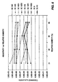
- Fig. 6 is a graph of selected OC coating compositions versus relative humidity.
-
- Fig. 1 shows a
color CRT 10 having aglass envelope 11 comprising arectangular faceplate panel 12 and atubular neck 14 connected by arectangular funnel 15. Thefunnel 15 has an internal conductive coating (not shown) that contacts ananode button 16 and extends into theneck 14. Thepanel 12 comprises aviewing faceplate 17 and a peripheral flange orsidewall 18, which is sealed to thefunnel 15 by a glass frit 19. As shown in Fig. 2, a relatively thin, light absorbingmatrix 20, having a plurality ofopenings 21, is provided on an interior surface of theviewing faceplate 17. A luminescent threecolor phosphor screen 22 is carried on the interior surface of thefaceplate 17 and overlies thematrix 20. Thescreen 22, preferably, is a line screen which includes a multiplicity of screen elements comprised of red-, blue-, and green-emitting phosphor stripes, R, B, and G, centered in different ones of the matrix openings and arranged in color groups or picture elements of three stripes or triads, in a cyclic order. The stripes extend in a direction that is generally normal to the plane in which the electron beams are generated. In the normal viewing position of the embodiment, the phosphor stripes extend in the vertical direction. Preferably, portions of the phosphor stripes overlap at least a portion of the lightabsorptive matrix 20 surrounding theopenings 21. Alternatively, a dot screen may be utilized. A thinconductive layer 24, preferably of aluminum, overlies thescreen 22 and provides means for applying a uniform potential to the screen, as well as for reflecting light, emitted from the phosphor elements, through thefaceplate 17. Thescreen 22 and theoverlying aluminum layer 24 comprise a screen assembly. Again with reference to Fig. 1, a multi-apertured color selection electrode, such as a shadow mask or focus mask, 25 is removably mounted, by conventional means, in predetermined spaced relation to the screen assembly. - An
electron gun 27, shown schematically by the dashed lines in Fig. 1, is centrally mounted within theneck 14, to generate and direct threeelectron beams 28 along convergent paths, through the apertures in thecolor selection electrode 25, to thescreen 22. The electron gun is conventional and may be any suitable gun known in the art. - The
tube 10 is designed to be used with an external magnetic deflection yoke, such asyoke 30, located in the region of the funnel-to-neck junction. When activated, theyoke 30 subjects the threebeams 28 to magnetic fields that cause the beams to scan horizontally and vertically, in a rectangular raster, over thescreen 22. The initial plane of deflection (at zero deflection) is shown by the line P - P in Fig. 1, at about the middle of theyoke 30. For simplicity, the actual curvatures of the deflection beam paths, in the deflection zone, are not shown. - The
screen 22 is manufactured by an electrophotographic screening (EPS) process that is described in U.S. Pat. No. 4,921,767, issued to Datta et al. on May 1, 1990. With reference to Fig. 3, step 31, thepanel 12 is cleaned by washing it with a caustic solution, rinsing it in water, etching it with buffered hydrofluoric acid and rinsing it again with water, as is known in the art. Then, as indicated instep 33, the interior surface of theviewing faceplate 17 is provided with thelight absorbing matrix 20, preferably, using the conventional wet matrix process described in U.S. Pat. No. 3,558,310, issued to Mayaud on Jan. 26, 1971. In the wet matrix process, a suitable photoresist solution is applied to the interior surface, e.g., by spin coating, and the solution is dried to form a photoresist layer. Then, thecolor selection electrode 25 is inserted into thepanel 12 and the panel is placed onto a three-in-one lighthouse (not shown) which exposes the photoresist layer to actinic radiation from a light source which projects light through the openings in the color selection electrode. The exposure is repeated two more times with the light source located to simulate the paths of the electron beams from the three electron guns. The light selectively alters the solubility of the exposed areas of the photoresist layer. After the third exposure, the panel is removed from the lighthouse and the color selection electrode is removed from the panel. The photoresist layer is developed, using water, to remove the more soluble areas thereof, thereby exposing the underlying interior surface of the viewing faceplate, and leaving the less soluble, exposed areas of the photoresist layer intact. Then, a suitable solution of light-absorbing material is uniformly provided onto the interior surface of the faceplate panel to cover the exposed portion of the viewing faceplate and the retained, less soluble, areas of the photoresist layer. The layer of light-absorbing material is dried and developed using a suitable solution which will dissolve and remove the retained portion of the photoresist layer and the overlying light-absorbing material, forming theopenings 21 in thematrix 20 which is adhered to the interior surface of the viewing faceplate. The interior surface of theviewing faceplate 17, having thematrix 20 thereon, is then coated with a novel conductive solution, as indicated instep 35 to form alayer 32 of a volatilizable, organic conductive (OC) material, shown in Fig. 4. As indicated in Fig. 3,step 37 and shown in Fig. 4, theOC layer 32 provides an electrode for an overlying volatilizable, organic photoconductive (OPC)layer 34. TheOC layer 32 and theOPC layer 34, in combination, comprise aphotoreceptor 36, also shown in Fig. 4. - The
novel OC layer 32 is formed from a conductive solution comprising 3,4-polyethylene dioxythiophene polystyrene sulphonate (PEDT/PSS); a polymer or co-polymer selected from the group consisting of polyvinylpyrrolidone (PVP), poly (vinyl pyridine-co-vinyl acetate) (PVPy-VAc), polymethacrylic acid (PMAA), poly (hydroxyethylacrylate-co-methacrylic acid) (PHEA-MAA), poly (2-hydroxyethyl methacrylate) (PHEMA), polyvinylbutyral (PVB); and a suitable solvent, such as methanol. PEDT/PSS is available from Bayer Corporation, Pittsburgh, PA, under the tradename BAYTRON P, an emulsion in water (1.4% solid). The procedure for formulating an organic conductive solution, identified as OC-10K, is as follows: - prepare a 10% stock solution of PHEMA in methanol;
- prepare an 8:1 dilution of BAYTRON-P as a second stock solution;
- add 748 g of 10% PHEMA stock solution to a 1 gallon container;
- stir with a high speed mechanical stirrer;
- slowly add 1717.5 g of 8:1 BAYTRON-P stock solution to the container;
- add 100 g of PVP solution (purchased as a 20% aqueous solution);
- add 15 g of 100% L-10 surfactant;
- cover container and stir for 1 hour and check for undissolved solids;
- replace any methanol lost due to evaporation;
- add 855 g of acetone and stir in a covered container for 10 min.;
- filter solution using a 10 µm pre-filter and a 5 µm final filter; and
- store the OC-10K solution in a plastic bottle.
-
- The procedure for formulating an organic conductive solution, identified as OC-10-Ft3, is as follows:
- prepare a 5% stock solution of PHEMA in methanol;
- add 5.93 kg of methanol to a metal container;
- add 1.39 kg of 5% the PHEMA stock solution to the container,
- add 1.33Kg of 100% BAYTRON-P
- add 10 g or tetronic 901 stock solution (25% solids in methanol);
- stir the solution of at least 1 hour;
- replace evaporated methanol;
- filter through both 5 µm and 10 µm Millipore filters; and
- store the OC-10Ft3 solution in a plastic bottle.
-
- The 3,4-polyethylene dioxythiophene polystyrene sulphonate (PEDT/PSS) is diluted with various polymers in order to reduce the organic residue that remains after the resultant OC layer is baked out at 450 °C. The polymers or co-polymers that may be used for this purpose include: polyvinylpyrrolidone (PVP); poly (vinyl pyridine-co-vinyl acetate) (PVPy-VAc); polymethacrylic acid (PMAA); poly (hydroxyethylacrylate-co-methacrylic acid) (PHEA-MAA); poly (2-hydroxyethyl methacrylate) (PHEMA); and polyvinylbutyral (PVB). The resistivity of the
OC layer 32 with various polymers was determined and is summarized in TABLE 1. The data show that the resistivity of the composition increases by more than one order of magnitude when PEDT/PSS is diluted with different polymers.Identification Number Coating Composition Resistivity (MΩ/Sq.) OC-10 100% PEDT/PSS 0.4 - 0.7 OC-10A 31% PEDT/PSS;69%PVP 2 - 4 OC-10C 31% PEDT/PSS; 69% PMAA 1.7 OC-10C-1 58% PEDT/PSS; 42% PMAA 1.0 OC-10C-2 13% PEDT/PSS; 87% PMAA 5.0 OC-10D 31% PEDT/PSS; 69% VP-VA 2.8 OC-10D-1 58% PEDT/PSS; 42% VP-VA 1.2 OC-10D-2 13% PEDT/PSS; 87% VP-VA 6.0 OC-10E 31%PEDT/PSS; 69% HEA-MAA 5.7 OC-10E-1 58% PEDT/PSS; 42% HEA-MAA 2.5 OC-10E-2 13% PEDT/PSS; 87% HEM-MAA 24.0 OC- 10Ft3 20% PEDT/PSS; 80% PHEMA 1.5 OC-10K 3% PEDT/PSS; 76% PHEMA; 21% PVP 9.0 - With respect to OC-10K, the composition includes: 3% PEDT/PSS as the active ingredient; about 76% PHEMA to facilitate bakeout; about 21% PVP as a thickening or 5 viscosity adjusting agent; and about 0.05% Pluronic L-10, or less, available from BASF, Mt. Olive, NJ, as a surfactant. Additionally, acetone may comprise 10 - 30% of the total mass of the mixture as an anti-foaming agent. The viscosity of the composition is within the range of 15 - 30 cP and the Pluronic L-10 should be within the range of 0.01 to 1.0% to coalesce the OC film while drying.
- Composition OC-10Ft3 includes: 20% PEDT/PSS as the active ingredient; about 80% PHEMA to facilitate bakeout; and about 0.05% Tetronic 901, available from BASF, Mt. Olive, NJ, as a surfactant.
- As indicated in
step 39 of Figure 3, theOPC layer 34 of thephotoreceptor 36, is corona charged using the charging apparatus described in U.S. Pat. No. 5,519,217, issued on May 21, 1996 to Wilbur, Jr. et al., to establish a substantially uniform charge thereon. Figure 5 shows a graph of the corona charging rate for several combinations of OC-8 (Luviquat MS-905) overcoated with OPC's 6 and 7 and the present OC-10E (PEDT/PSS), also with OPC's 6 and 7. - The
OPC layer 34 is formed by overcoating theOC layer 32 with an organic photoconductive solution comprising a suitable resin, an electron donor material, an electron acceptor material, a surfactant and an organic solvent. - The solution for OPC-6 contains the following ingredients:
- 2640 g (87.34 wt. %) of xylene;
300 g (9.93 wt. %) of polystyrene, available from Amoco Corp., Chicago, IL, as Amoco IR7C7; - 15 g (0.5 wt. %) of dioctylphthalate (DOP);
- 50 g (1.65 wt. %) of 1,4-(2,4-dimethylphenyl) 1,4 diphenylbutatriene ((2,4 DMPBT);
- 15 g (0.5 wt. %) of 2-ethylanthraquinone (EAQ);
- 2.5 g (0.08 wt. %) of 2,4,7-trinitro-9-fluorenone (TNF); and
- 0.15 g (trace) of surfactant UL-7602, available from Union Carbide, Danbury, CT.
-
- OPC-6 may be applied by spin coating; however, if it is desired to electrostatically spray the OPC solution onto the OC layer, a 3:1 xylene-toluene solvent ratio may be used, rather than all xylene. OPC-6 is formulated as follows:
- the solvent(s) is added to a 6 quart stainless steel beaker and mechanically stirred and heated to 45°C;
- the polystyrene is added in small quantities until all of the styrene goes into solution; and the stirring is continued until all of the polystyrene is dissolved;
- the heat is turned off, and the DOP is added;
- the 2,4 (DMPBT) is added while the stirring is continued;
- the EAQ is added, while stirring;
- the TNF is added, while stirring; and
- the UL-7602 is added.
-
- Stirring is continued overnight (for at least 12 hours) and then the solution is filtered through a cascade of Millipore filters.
- The solution for OPC-7 contains the following ingredients:
- 2048 g (63.3 wt. %) of toluene and 792 g of xylene;
- 792 g (24.5 wt. %) of xylene;
- 300 g (9.3 wt. %) of polystyrene;
- 75 g (2.3 wt. %) of tetraphenylethylene (TPE);
- 11.25 g (0.35 wt. %) of EAQ;
- 7.5 g (0.23 wt. %) of TNF; and
- 0.15 g (trace) of UL-7602.
-
- The procedure for formulating OPC-7 is similar to that for formulating OPC-6, except that after the surfactant, UL-7602, is added to the solution, the stirring need only be continued for 2-3 hours, until all the materials are dissolved.
- The samples shown in Figure 5 were prepared by coating OC-10E and OC-8 on 3 inch by 3 inch (1.2 cm x 1.2 cm) glass slides. The thickness of the OC layers is 1±0.2 µm. The glass slides with the OC's were coated with OPC-6 and OPC-7. The thickness of the OPC-6 and OPC-7 are respectively 4.5 and 5 µm. The photoconductivity of OC-10E and OC-8 with the OPC's was determined at different values of relative humidity (RH). The glass slides with OC-10E and different OPC's were stored in a humidity-controlled chamber for one hour before photoconductivity measurements were taken. The OPC/OC samples were corona charged for 25 seconds and the voltage was recorded each second. The corona charging rate was determined from the voltage time plot. The charging rate was calculated for OPC-6 and OPC-7 on OC-10E and compared with charging rates of the same OPC's on OC-8. The results of charging rate measurements taken at various values of relative humidity are plotted in Figure 5. The results show that corona charging rate of OPC-6 and OPC-7 on the present OC-10E (PEDT/PSS) is twice as fast as the same OPC's on the prior OC-8. The charging rate of the OPC's on OC-10E is less dependent on humidity but the charging rate is lower below 40% RH. These results indicate that OC-10E has better processing latitude than the standard OC-8.
- The dark decay and the photo decay of OPC-6 and OPC-7 on OC-8 and OC-10E are summarized in TABLE 2. The OPC/OC combinations, after corona charging for 30 seconds, were kept in the dark for 90 seconds and the voltage on the OPC/OC was recorded every 1 second at relative humidities of 30 and 55 percent (% RH) to determine dark decay. Then, the OPC/OC samples were recharged and, after 90 seconds in the dark, were exposed to 5 xenon light pulses and the voltage on the OPC/OC samples was recorded after each pulse at relative humidities of 30 and 55 % RH to determine photo decay.
OPC/OC % RH Dark Decay (V/sec) % Photo Decay OPC-6/OC- 10E 30 0.4 97 55 0.9 98 OPC-6/OC-8 30 0.3 95 55 1.0 94 OPC-7/OC- 10E 30 0.2 89 55 0.8 87 OPC-7/OC-8 30 0.2 86 55 1.0 85 - The thermal decomposition properties of selected ones of the compositions listed in TABLE 1 have been determined using thermogravimetric analysis (TGA). The samples were heated from room temperature to 440°C at a rate of 1°C/min. and then maintained at 440°C for 60 minutes. The results are summarized in TABLE 3. The polymer PEDT/PSS, without additives, has about 15% of the organic materials remaining after the bakeout process; however, for OC-10E, the additive HEA-MAA reduces the residue of the PEDT/PSS materials to less than 1%.
Identification Number Coating Composition % Residue OC-10 (Bayer) 100% PEDT/ PSS 15 OC-10C 31% PEDT/PSS;
69% PMAA4 OC-10D 31% PEDT/PSS;
69% PVPy-VAc6 OC-10E 31% PEDT/PSS;
69% PHEA-MAA<1 OC- 10Ft3 20% PEDT/PSS;
80% PHEMA4 OC-10K 3% PEDT/PSS;
76% PHEMA; 21% PVP4 - The sheet resistivity in ohms/square (Ω/□) of the various coating compositions, at different relative humidity (RH) and at a temperature of 20°C, is listed in TABLE 4.
ID# Coating Composition 21% RH 34% RH 55% RH 65% RH OC-8 MS-905 4.7E+09 5.0E+07 6.4E+07 1.3E+07 OC-10 100% PEDT/PSS 1.1E+05 1.2E+05 7.0E+05 4.0E+04 OC-10C 31% PEDT/PSS; 69% PMAA 3.3E+05 2.0E+05 1.7E+05 1.5E+05 OC-10D 31%PEDT/PSS; 69%PVPy-VAc 1.35E+08 1.6E+07 2.8E+06 3.4E+05 OC-10D1 13%PEDT/PSS; 87%PVPy-VAc 4.7E+09 1.8E+08 5.0E+07 2.6E+07 OC-10D2 58%PEDT/PSS; 42% PVPy-VAc 1.6E+04 1.2E+05 1.0E+06 1.0E+05 OC-10E 31%PEDT/PSS; 60%PHEA-MAA 8.8E+07 6.8E+07 5.7E+07 5.4E+07 OC-10E1 13%PEDT/PSS; 87%PHEA-MAA 3.3E+08 3.2E+08 2.4E+08 1.6E+08 OC-10E2 58%PEDT/PSS; 42%PHEA-MAA 5.0E+06 3.8E+05 2.5E+06 2.7E+05 OC-10Ft3 20%PEDT/PSS; 80%PHEMA N/A* N/A* 1.5E+06 N/A OC-10K 3%PEDT/PSS; 76%PHEMA; 21%PVP N/A* N/A* 9.0E+06 N/A* - From TABLE 4 it can be seen that for OC-10, which is pure PEDT/PSS, and for OC-10D2 and OC-10E2 in which the concentration of PEDT/PSS is 58%, there is an irregular interaction with humidity; however, for samples OC-10E and OC-10E1, as the concentration of PEDT/PSS increases, the resistivity decreases so slightly that these compositions can be termed humidity insensitive. The single coating concentration of OC-10C that was tested also showed only a slight decrease in resistivity with increasing humidity, however no conclusions can be drawn from one sample. For samples OC-10D and OC-10D1, however, as the concentration of PEDT/PSS increases the resistivity decreases with increasing humidity at a somewhat greater extent than for samples OC-10E and OC-10E1. For samples OC-10Ft3 and OC-10K, only a single concentration was tested at 55%RH and no conclusions can be drawn. Because samples OC-10C, OC10E, and OC-10E1 exhibit little change in resistivity as the humidity increases, it can be concluded that a proper mixture of PEDT/PSS and one of the polymers mentioned in TABLE 4 can produce an organic polymer that is relatively insensitive to changes in humidity. The results of selected coating compositions listed in TABLE 4 versus relative humidity are shown in Fig. 6.
- After the
OPC layer 34 of thephotoreceptor 36 is electrostatically charged to a voltage within the range of approximately +200 to +700 volts, thecolor selection electrode 25 is then inserted into thepanel 12 and placed onto a lighthouse (not shown). The positively chargedOPC layer 34 of thephotoreceptor 36 is exposed, as indicated instep 41 of Fig. 3, through thecolor selection electrode 25, to light from a xenon flash lamp, or other light source of sufficient intensity, such as a mercury arc, disposed within the lighthouse. The light which passes through the apertures in thecolor selection electrode 25, at an angle identical to that of one of the electron beams from the electron gun of the tube, discharges selected illuminated areas of theOPC layer 34 and forms a latent charge image (not shown). Thecolor selection electrode 25 is removed from thepanel 12 and the panel is placed onto a first phosphor developer ( also not shown). The latent charge on theOPC layer 34 is developed, as indicated by step 43. The charging, exposing and phosphor developing steps, 39, 41 and 43, respectively, are repeated a total of three times to form the three-color phosphor screen 22. The three phosphors are fixed to minimize displacement, as indicated in step 45 of Fig. 3, to theOPC layer 34 of thephotoreceptor 36 by contacting the phosphor materials with the vapor of a suitable solvent, in the manner described in U.S. Pat. No. 4,917,978, issued to Ritt et al. on April 17, 1990. The screen structure is then spray-filmed and aluminized, as indicated insteps
Claims (3)
- A method of manufacturing a luminescent screen assembly on an interior surface of faceplate panel (17) for a color CRT (10) comprising the steps of coating said surface of said panel with a conductive solution to form a volatilizable organic conductive layer (32), and overcoating said organic conductive layer with a photoconductive solution to form a volatilizable photoconductive layer (34); characterized in that said conductive solution comprises: 3,4-polyethylene dioxythiophene polystyrene sulphonate (PEDT/PSS); a polymer or co-polymer selected from the group consisting of polyvinylpyrrolidone (PVP), poly (vinyl pyridine-co-vinyl acetate) (PVPy-VAc), polymethacrylic acid (PMAA), poly (hydroxyethylacrylate-co-methacrylic acid) (PHEA-MAA) poly (2-hydroxyethyl methacrylate) (PHEMA), and polyvinylbutyral (PVB); and a suitable solvent.
- A method of manufacturing a luminescent screen assembly on an interior surface of a faceplate panel (17) for a color CRT (10), comprising the steps of:a) coating said surface of said panel with a conductive solution to form a volatilizable organic conductive layer (32);b) overcoating said organic conductive layer with a photoconductive solution to form a volatilizable organic photoconductive layer (34);c) establishing a substantially uniform electrostatic charge on said photoconductive layer,d) exposing selected areas of said photoconductive layer to actinic radiation to affect the charge thereon;e) developing said photoconductive layer with at least on dry-powdered, light emitting, triboelectrically charged screen structure material;f) fixing said screen structure material to said photoconductive layer to minimize displacement thereof;g) filming said fixed screen structure material to form a film layer thereon;h) aluminizing said filmed layer; andi) baking said faceplate panel in air at a temperature of at least 450 °C. to volatilize the constituents of said screen assembly, including said organic conductive layer, said organic photoconductive layer and said film layer; characterized in that said conductive solution comprises: 3,4-polyethylene dioxythiophene polystyrene sulphonate (PEDT/PSS); a polymer or co-polymer selected from the group consisting of polyvinylpyrrolidone (PVP), poly (vinyl pyridine-co-vinyl acetate) (PVPy-VAc), polymethacrylic acid (PMAA), poly (hydroxyethylacrylate-co-methacrylic acid) (PHEA-MAA), poly (2-hydroxyethyl methacrylate) (PHEMA) and polyvinylbutyral (PVB) to reduce residue after said baking step; and a suitable solvent.
- The method as described in claim 2, characterized in that said conductive solution further comprises a surfactant, an anti-foaming agent and deionized water.
Applications Claiming Priority (2)
| Application Number | Priority Date | Filing Date | Title |
|---|---|---|---|
| US379161 | 1999-08-23 | ||
| US09/379,161 US6326110B1 (en) | 1999-08-23 | 1999-08-23 | Humidity and temperature insensitive organic conductor for electrophotographic screening process |
Publications (3)
| Publication Number | Publication Date |
|---|---|
| EP1079411A2 EP1079411A2 (en) | 2001-02-28 |
| EP1079411A3 EP1079411A3 (en) | 2002-01-09 |
| EP1079411B1 true EP1079411B1 (en) | 2003-11-12 |
Family
ID=23496069
Family Applications (1)
| Application Number | Title | Priority Date | Filing Date |
|---|---|---|---|
| EP00402313A Expired - Lifetime EP1079411B1 (en) | 1999-08-23 | 2000-08-18 | Electrophotographic screening method with humidity and temperature insensitive organic conductor |
Country Status (9)
| Country | Link |
|---|---|
| US (1) | US6326110B1 (en) |
| EP (1) | EP1079411B1 (en) |
| JP (1) | JP3716167B2 (en) |
| KR (1) | KR100575405B1 (en) |
| CN (1) | CN1216396C (en) |
| DE (1) | DE60006463T2 (en) |
| MX (1) | MXPA00008265A (en) |
| MY (1) | MY127756A (en) |
| TW (1) | TWI230966B (en) |
Cited By (1)
| Publication number | Priority date | Publication date | Assignee | Title |
|---|---|---|---|---|
| US7192910B2 (en) | 2003-10-28 | 2007-03-20 | Sachem, Inc. | Cleaning solutions and etchants and methods for using same |
Families Citing this family (3)
| Publication number | Priority date | Publication date | Assignee | Title |
|---|---|---|---|---|
| KR20050119906A (en) * | 2004-06-17 | 2005-12-22 | 삼성에스디아이 주식회사 | Method for manufacturing phosphors structure |
| WO2012039240A1 (en) * | 2010-09-24 | 2012-03-29 | コニカミノルタホールディングス株式会社 | Method for producing transparent electrode and organic electronic device |
| WO2022239107A1 (en) * | 2021-05-11 | 2022-11-17 | シャープディスプレイテクノロジー株式会社 | Light-emitting element, light-emitting device, and method for manufacturing light-emitting element |
Family Cites Families (16)
| Publication number | Priority date | Publication date | Assignee | Title |
|---|---|---|---|---|
| US3558310A (en) | 1967-03-29 | 1971-01-26 | Rca Corp | Method for producing a graphic image |
| US4921767A (en) | 1988-12-21 | 1990-05-01 | Rca Licensing Corp. | Method of electrophotographically manufacturing a luminescent screen assembly for a cathode-ray-tube |
| US4917978A (en) | 1989-01-23 | 1990-04-17 | Thomson Consumer Electronics, Inc. | Method of electrophotographically manufacturing a luminescent screen assembly having increased adherence for a CRT |
| US5370952A (en) | 1993-12-22 | 1994-12-06 | Rca Thomson Licensing Corp. | Organic conductor for an electrophotographic screening process for a CRT |
| US5407765A (en) | 1993-12-22 | 1995-04-18 | Thomson Consumer Electronics, Inc. | Method of spray-depositing an organic conductor to make a screen assembly for a CRT |
| US5405722A (en) | 1993-12-22 | 1995-04-11 | Rca Thomson Licensing Corp. | Method for combined baking-out and sealing of an electrophotographically processed screen assembly for a cathode-ray tube |
| US5413885A (en) * | 1993-12-22 | 1995-05-09 | Rca Thompson Licensing Corp. | Organic photoconductor for an electrophotographic screening process for a CRT |
| US5519217A (en) | 1995-05-08 | 1996-05-21 | Thomson Consumer Electronics, Inc. | Apparatus for charging an organic photoconductive layer for a CRT |
| US5928821A (en) * | 1995-12-22 | 1999-07-27 | Thomson Consumer Electronics, Inc. | Method of manufacturing a phosphor screen for a CRT |
| KR100232577B1 (en) * | 1996-07-15 | 1999-12-01 | 김영남 | Photoconductive coating phosphor powder for manufacturing electrophotographical screen of crt and coating method of phosphor powder thereof |
| DE19630016C2 (en) * | 1996-07-25 | 2000-10-12 | Daimler Chrysler Ag | Method for producing a phosphor layer of a cathode ray tube |
| GB9624706D0 (en) * | 1996-11-28 | 1997-01-15 | Cambridge Display Tech Ltd | Light emitting polymer device |
| KR100243254B1 (en) * | 1996-12-13 | 2000-02-01 | 손욱 | Composition for transparent conductive layer, manufacturing method of transparent conductive layer and surface conductive articles |
| US5840450A (en) * | 1996-12-24 | 1998-11-24 | Samsung Display Devices Co., Ltd. | Method for forming a black matrix on a faceplate panel for a color CRT |
| KR20000011267A (en) * | 1998-07-24 | 2000-02-25 | 김영남 | Screen display faceplate on which conductive organic polymeric transparent anti-static film is formed, its solution and its manufacturing method |
| US5925485A (en) * | 1998-08-05 | 1999-07-20 | Thomson Consumer Electronics, Inc. | Method of manufacturing a phosphor screen for a CRT |
-
1999
- 1999-08-23 US US09/379,161 patent/US6326110B1/en not_active Expired - Fee Related
-
2000
- 2000-08-18 EP EP00402313A patent/EP1079411B1/en not_active Expired - Lifetime
- 2000-08-18 DE DE60006463T patent/DE60006463T2/en not_active Expired - Fee Related
- 2000-08-18 JP JP2000248815A patent/JP3716167B2/en not_active Expired - Fee Related
- 2000-08-22 MY MYPI20003859A patent/MY127756A/en unknown
- 2000-08-23 KR KR1020000048864A patent/KR100575405B1/en not_active Expired - Fee Related
- 2000-08-23 CN CN001306731A patent/CN1216396C/en not_active Expired - Fee Related
- 2000-08-23 MX MXPA00008265A patent/MXPA00008265A/en active IP Right Grant
- 2000-08-24 TW TW089117074A patent/TWI230966B/en not_active IP Right Cessation
Cited By (1)
| Publication number | Priority date | Publication date | Assignee | Title |
|---|---|---|---|---|
| US7192910B2 (en) | 2003-10-28 | 2007-03-20 | Sachem, Inc. | Cleaning solutions and etchants and methods for using same |
Also Published As
| Publication number | Publication date |
|---|---|
| MY127756A (en) | 2006-12-29 |
| EP1079411A3 (en) | 2002-01-09 |
| EP1079411A2 (en) | 2001-02-28 |
| DE60006463T2 (en) | 2004-10-14 |
| KR20010030120A (en) | 2001-04-16 |
| CN1288248A (en) | 2001-03-21 |
| JP3716167B2 (en) | 2005-11-16 |
| US6326110B1 (en) | 2001-12-04 |
| JP2001167702A (en) | 2001-06-22 |
| TWI230966B (en) | 2005-04-11 |
| KR100575405B1 (en) | 2006-05-03 |
| CN1216396C (en) | 2005-08-24 |
| DE60006463D1 (en) | 2003-12-18 |
| MXPA00008265A (en) | 2002-04-24 |
Similar Documents
| Publication | Publication Date | Title |
|---|---|---|
| EP0378911B1 (en) | Method of electrophotographically manufacturing a luminescent screen assembly for a cathode-ray tube | |
| EP0380279B1 (en) | Method of electrophotographically manufacturing a luminescent screen assembly for a color cathode-ray tube | |
| US5405722A (en) | Method for combined baking-out and sealing of an electrophotographically processed screen assembly for a cathode-ray tube | |
| US5413885A (en) | Organic photoconductor for an electrophotographic screening process for a CRT | |
| US5370952A (en) | Organic conductor for an electrophotographic screening process for a CRT | |
| KR100199887B1 (en) | CALTI Electrophotographic Screen Manufacturing Method Using Organic Photoconductive Layer | |
| US5135826A (en) | Method of electrophotographically manufacturing a luminescent screen assembly for a crt using an improved plasticizer for a photoconductive layer | |
| US6326110B1 (en) | Humidity and temperature insensitive organic conductor for electrophotographic screening process | |
| EP0375229B1 (en) | Surface treatment of phosphor particles and method for a crt screen | |
| US5455133A (en) | Method of manufacturing a screen assembly having a planarizing layer | |
| US5407765A (en) | Method of spray-depositing an organic conductor to make a screen assembly for a CRT | |
| US6040097A (en) | Solution for making photoconductive layer and an electrophotographic manufacturing method of the layer in CRT | |
| WO2000008669A1 (en) | Method of manufacturing a phosphor screen for a crt | |
| WO1998024109A1 (en) | A solution for making a photoconductive layer for a crt and their electrophotographical manufacture |
Legal Events
| Date | Code | Title | Description |
|---|---|---|---|
| PUAI | Public reference made under article 153(3) epc to a published international application that has entered the european phase |
Free format text: ORIGINAL CODE: 0009012 |
|
| AK | Designated contracting states |
Kind code of ref document: A2 Designated state(s): AT BE CH CY DE DK ES FI FR GB GR IE IT LI LU MC NL PT SE Kind code of ref document: A2 Designated state(s): DE FR GB IT |
|
| AX | Request for extension of the european patent |
Free format text: AL;LT;LV;MK;RO;SI |
|
| PUAL | Search report despatched |
Free format text: ORIGINAL CODE: 0009013 |
|
| AK | Designated contracting states |
Kind code of ref document: A3 Designated state(s): AT BE CH CY DE DK ES FI FR GB GR IE IT LI LU MC NL PT SE |
|
| AX | Request for extension of the european patent |
Free format text: AL;LT;LV;MK;RO;SI |
|
| 17P | Request for examination filed |
Effective date: 20020702 |
|
| AKX | Designation fees paid |
Free format text: DE FR GB IT |
|
| GRAH | Despatch of communication of intention to grant a patent |
Free format text: ORIGINAL CODE: EPIDOS IGRA |
|
| GRAS | Grant fee paid |
Free format text: ORIGINAL CODE: EPIDOSNIGR3 |
|
| GRAA | (expected) grant |
Free format text: ORIGINAL CODE: 0009210 |
|
| AK | Designated contracting states |
Kind code of ref document: B1 Designated state(s): DE FR GB IT |
|
| REG | Reference to a national code |
Ref country code: GB Ref legal event code: FG4D |
|
| REF | Corresponds to: |
Ref document number: 60006463 Country of ref document: DE Date of ref document: 20031218 Kind code of ref document: P |
|
| REG | Reference to a national code |
Ref country code: IE Ref legal event code: FG4D |
|
| ET | Fr: translation filed | ||
| PLBE | No opposition filed within time limit |
Free format text: ORIGINAL CODE: 0009261 |
|
| STAA | Information on the status of an ep patent application or granted ep patent |
Free format text: STATUS: NO OPPOSITION FILED WITHIN TIME LIMIT |
|
| 26N | No opposition filed |
Effective date: 20040813 |
|
| REG | Reference to a national code |
Ref country code: IE Ref legal event code: MM4A |
|
| PGFP | Annual fee paid to national office [announced via postgrant information from national office to epo] |
Ref country code: DE Payment date: 20080825 Year of fee payment: 9 |
|
| PGFP | Annual fee paid to national office [announced via postgrant information from national office to epo] |
Ref country code: IT Payment date: 20080828 Year of fee payment: 9 |
|
| PGFP | Annual fee paid to national office [announced via postgrant information from national office to epo] |
Ref country code: GB Payment date: 20080718 Year of fee payment: 9 |
|
| PGFP | Annual fee paid to national office [announced via postgrant information from national office to epo] |
Ref country code: FR Payment date: 20090821 Year of fee payment: 10 |
|
| GBPC | Gb: european patent ceased through non-payment of renewal fee |
Effective date: 20090818 |
|
| PG25 | Lapsed in a contracting state [announced via postgrant information from national office to epo] |
Ref country code: DE Free format text: LAPSE BECAUSE OF NON-PAYMENT OF DUE FEES Effective date: 20100302 |
|
| PG25 | Lapsed in a contracting state [announced via postgrant information from national office to epo] |
Ref country code: GB Free format text: LAPSE BECAUSE OF NON-PAYMENT OF DUE FEES Effective date: 20090818 |
|
| PG25 | Lapsed in a contracting state [announced via postgrant information from national office to epo] |
Ref country code: IT Free format text: LAPSE BECAUSE OF NON-PAYMENT OF DUE FEES Effective date: 20090818 |
|
| REG | Reference to a national code |
Ref country code: FR Ref legal event code: ST Effective date: 20110502 |
|
| PG25 | Lapsed in a contracting state [announced via postgrant information from national office to epo] |
Ref country code: FR Free format text: LAPSE BECAUSE OF NON-PAYMENT OF DUE FEES Effective date: 20100831 |