EP1079363A2 - Driving method for liquid crystal device - Google Patents
Driving method for liquid crystal device Download PDFInfo
- Publication number
- EP1079363A2 EP1079363A2 EP00307292A EP00307292A EP1079363A2 EP 1079363 A2 EP1079363 A2 EP 1079363A2 EP 00307292 A EP00307292 A EP 00307292A EP 00307292 A EP00307292 A EP 00307292A EP 1079363 A2 EP1079363 A2 EP 1079363A2
- Authority
- EP
- European Patent Office
- Prior art keywords
- liquid crystal
- tilt angle
- crystal device
- saturation
- voltage
- Prior art date
- Legal status (The legal status is an assumption and is not a legal conclusion. Google has not performed a legal analysis and makes no representation as to the accuracy of the status listed.)
- Withdrawn
Links
Images



Classifications
-
- G—PHYSICS
- G09—EDUCATION; CRYPTOGRAPHY; DISPLAY; ADVERTISING; SEALS
- G09G—ARRANGEMENTS OR CIRCUITS FOR CONTROL OF INDICATING DEVICES USING STATIC MEANS TO PRESENT VARIABLE INFORMATION
- G09G3/00—Control arrangements or circuits, of interest only in connection with visual indicators other than cathode-ray tubes
- G09G3/20—Control arrangements or circuits, of interest only in connection with visual indicators other than cathode-ray tubes for presentation of an assembly of a number of characters, e.g. a page, by composing the assembly by combination of individual elements arranged in a matrix no fixed position being assigned to or needed to be assigned to the individual characters or partial characters
- G09G3/34—Control arrangements or circuits, of interest only in connection with visual indicators other than cathode-ray tubes for presentation of an assembly of a number of characters, e.g. a page, by composing the assembly by combination of individual elements arranged in a matrix no fixed position being assigned to or needed to be assigned to the individual characters or partial characters by control of light from an independent source
- G09G3/36—Control arrangements or circuits, of interest only in connection with visual indicators other than cathode-ray tubes for presentation of an assembly of a number of characters, e.g. a page, by composing the assembly by combination of individual elements arranged in a matrix no fixed position being assigned to or needed to be assigned to the individual characters or partial characters by control of light from an independent source using liquid crystals
- G09G3/3611—Control of matrices with row and column drivers
- G09G3/3648—Control of matrices with row and column drivers using an active matrix
- G09G3/3651—Control of matrices with row and column drivers using an active matrix using multistable liquid crystals, e.g. ferroelectric liquid crystals
-
- G—PHYSICS
- G09—EDUCATION; CRYPTOGRAPHY; DISPLAY; ADVERTISING; SEALS
- G09G—ARRANGEMENTS OR CIRCUITS FOR CONTROL OF INDICATING DEVICES USING STATIC MEANS TO PRESENT VARIABLE INFORMATION
- G09G3/00—Control arrangements or circuits, of interest only in connection with visual indicators other than cathode-ray tubes
- G09G3/20—Control arrangements or circuits, of interest only in connection with visual indicators other than cathode-ray tubes for presentation of an assembly of a number of characters, e.g. a page, by composing the assembly by combination of individual elements arranged in a matrix no fixed position being assigned to or needed to be assigned to the individual characters or partial characters
- G09G3/34—Control arrangements or circuits, of interest only in connection with visual indicators other than cathode-ray tubes for presentation of an assembly of a number of characters, e.g. a page, by composing the assembly by combination of individual elements arranged in a matrix no fixed position being assigned to or needed to be assigned to the individual characters or partial characters by control of light from an independent source
- G09G3/36—Control arrangements or circuits, of interest only in connection with visual indicators other than cathode-ray tubes for presentation of an assembly of a number of characters, e.g. a page, by composing the assembly by combination of individual elements arranged in a matrix no fixed position being assigned to or needed to be assigned to the individual characters or partial characters by control of light from an independent source using liquid crystals
-
- G—PHYSICS
- G09—EDUCATION; CRYPTOGRAPHY; DISPLAY; ADVERTISING; SEALS
- G09G—ARRANGEMENTS OR CIRCUITS FOR CONTROL OF INDICATING DEVICES USING STATIC MEANS TO PRESENT VARIABLE INFORMATION
- G09G2320/00—Control of display operating conditions
- G09G2320/04—Maintaining the quality of display appearance
- G09G2320/043—Preventing or counteracting the effects of ageing
Definitions
- the present invention relates to a driving method for liquid crystal device used as a light valve for use in a flat panel display, a projection display, a printer, etc.
- CRTs cathode ray tubes
- VTRs video tape recorders
- a CRT cathode ray tube
- a CRT is accompanied with various difficulties for static picture display, such as flickering, a low picture recognizability due to scanning fringes caused by insufficient resolution, and deterioration of the fluorescent screen due to sticking or burning.
- electromagnetic wave generated from CRTs can adversely affect the human body and health of VDT operators.
- a CRT necessarily requires a structure including a large volume behind the screen and is inconvenient from the viewpoints of effective utilization of data processing apparatus and space economization in offices and at home.
- a liquid crystal display device is known to solve these difficulties of CRTs.
- a type of liquid crystal device using a twisted nematic (TN)-type liquid crystal as disclosed by M. Schadt and W. Helfrich, Applied Physics Letters, Vol. 18, No. 4 (February 15, 1971), pp. 127 - 128.
- TFTs thin film transistors
- This type of device uses a transistor for each pixel, is free from crosstalk problem and is being produced at a fairly good productivity for display sizes of 10 - 12 inches (in diagonal) owing to rapid progress in semiconductor production technology.
- the TFT-type device still leaves some difficulties, such as response speed of a liquid crystal material.
- a chiral smectic liquid crystal device of the type utilizing bistability of liquid crystal molecules has been proposed by Clark and Lagerwall (U.S. Patent No. 4,367,924; Japanese Laid-Open Patent Application (JP-A) 56-107216).
- the liquid crystal molecules cause switching in plane with respect to substrates, thus being expected to achieve remarkable improvement in viewing angle characteristic.
- the chiral smectic liquid crystal also exhibits a very quick response speed because of inversion switching thereof based on its spontaneous polarization.
- a chiral smectic anti-ferroelectric liquid crystal device has been proposed recently by Chandani, Takezoe, et al.
- a ferroelectric liquid crystal (FLC) having a single stable state (monostable state) a Half V-shaped mode FLC exhibiting an asymmetric V-T characteristic depending on a polarity of an applied voltage proposed by Asao et al. (Journal of Applied Physics, vol. 38 (1999), p. 5977-) and an FLC exhibiting a V-shaped response characteristic proposed by Nito, Imanishi, et al. (Shinkaku Giho (TECHNICAL REPORT OF IEICE), EID 96 - 176, OME 96 - 94 (1997)) have been known.
- These FLCs are suitable for a display mode allowing a high-speed gradation control and a decreased spontaneous polarization, thus being suitable as a liquid crystal material for drive using active elements such as TFTs.
- Such active matrix-type liquid crystal devices using a chiral smectic liquid crystal having (anti-)ferroelectricity has still left problems in terms of deterioration in display characteristics due to burning or sticking and/or a change in alignment state of the liquid crystal in a long term drive.
- Embodiments of the present invention provide a driving method for a liquid crystal device which alleviates the above-mentioned problems.
- One embodiment of the present invention provides a driving method for a chiral smectic liquid crystal device of an active matrix type which stably provides good gradational images for a long period.
- a driving method for a liquid crystal device of the type comprising a pair of oppositely disposed substrates each provided with an electrode, a chiral smectic liquid crystal disposed between the substrates to form a plurality of pixels, and a plurality of active elements each of which is provided to an associated pixel and is connected with an associated electrode so as to effect a matrix drive of the liquid crystal device, the liquid crystal being placed in a monostable state under no voltage application; the method comprising: a step of driving the liquid crystal device so that the liquid crystal is tilted from the monostable state to provide a maximum tilt angle in actual drive smaller than a saturation tilt angle.
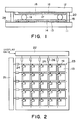
- Figure 1 is a schematic sectional view of an embodiment of the liquid crystal device of the present invention.
- Figure 2 is a schematic plan view of an embodiment of an active matrix substrate of the liquid crystal device shown in Figure 1 in combination with peripheral drive circuits.
- Figure 3 is a block diagram of a liquid crystal display apparatus including as a display panel the liquid crystal device according to the present invention and a graphic controller.
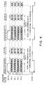
- Figure 4 is a time chart illustrating a manner of image data communication between the liquid crystal display apparatus and the graphic controller shown in Figure 3.
- Figure 5 is an equivalent circuit diagram of a liquid crystal device of an active matrix-type used in Examples.
- Figure 6 is a schematic view for illustrating a deformation of layer structure in smectic phase in a chiral smectic liquid crystal device.
- Figure 7 is a schematic sectional view for illustrating a surface disclination in a chiral smectic liquid crystal device.
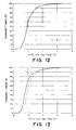
- FIGS 8, 9, 10, 12 and 13 are graphs showing V-T characteristics of liquid crystal devices used in Example 1, Example 2, Comparative Example 1, Example 3 and Comparative Example 2, respectively, appearing hereinafter.
- FIG. 11 is a graph showing an optical response (V-T) characteristic of liquid crystal devices used in Example 3.
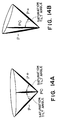
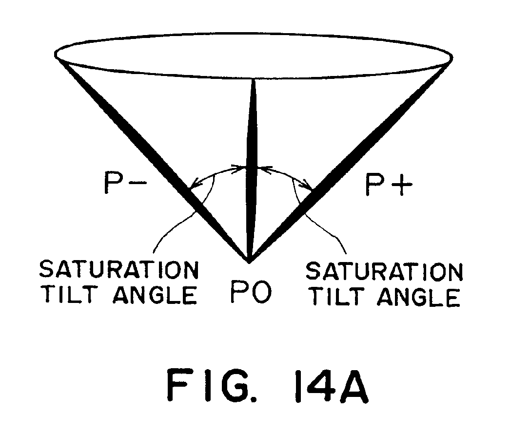
- Figures 14A and 14B are schematic views for illustrating saturation tilt angles of liquid crystal molecules providing a V-shaped response characteristic and a Half V-shaped response characteristic, respectively.
- the burning phenomenon has been noticeably observed in such an alignment mode that liquid crystal molecules located in the vicinity of boundaries with substrates are inverted depending on ON/OFF state of a chiral smectic liquid crystal device.
- This inversion behavior is a switching accompanied with inversion of domain wall (domain inversion), i.e., a switching such that, when viewed from the substrate side, either one of a white (display) region or a black (display) region is broadened or narrowed while keeping a boundary (wall) therebetween.
- domain inversion domain wall
- the inversion behavior refers to an inversion accompanied with a surface disclination as shown in Figure 7.
- Figure 6 shows positions (directions) of C-directors in smectic phase of liquid crystal molecules in a chiral smectic liquid crystal device having a cell structure providing a chevron (layer) structure.
- At (A) is shown those under no voltage application, and at (B) is shown those under application of a high voltage.
- a left-hand view illustrates C-directors viewed from a direction perpendicular to smectic (molecular) layers (a smectic layer normal direction) and a right-hand view illustrates liquid crystal molecules viewed from a direction of smectic layers (a smectic layer direction).
- liquid crystal molecules 62 are oriented or aligned while providing C-directors 63 and directions 64 of spontaneous polarization.
- the directions 64 of spontaneous polarization at a (mid or intermediate) kink portion of the smectic layer are not perpendicular to the surfaces of the substrates 61a and 61b, thus deviating from a direction normal to the substrates.
- the state (at (B)) is a state such that a layer inclination angle (6) at the kink portion becomes small, i.e., a deformed state of a layer structure in smectic phase. If such a deformed state is continued for a long time, the deformed layer structure remains as a structural history even when the applied electric field is removed, thus resulting in a change in electro-optical response characteristic.
- a maximum tilt angle at the time of actual drive is below (e.g., at most 95 % of) a saturation tilt angle of a liquid crystal material used, it has become possible to prevent application of an excessive electric field for the actual drive of the liquid crystal device, thus suppressing an occurrence of burning and/or deformation of layer structure to realize stable display performances.
- the maximum tilt angle is controlled to be smaller than, preferably at most 95 % of, more preferably at most 90 % of, further preferably at most 80 % of, the saturation tilt angle.
- a particular control means is not necessarily required. More specifically, the control of the maximum tilt angle in actual drive to be smaller than the saturation tilt angle may be effected by preliminarily setting an applied (operating) voltage to the extent that liquid crystal molecules are not tilted from their monostable position (at the time of no voltage application) to their extreme position providing the saturation tilt angle.
- the chiral smectic liquid crystal device may appropriately be designed so that liquid crystal molecules do not move up to their extreme position under voltage application. In other words, the liquid crystal device does not provide the saturation tilt angle at the time of actual drive thereof.
- liquid crystal device driven by the driving method according to one embodiment of the invention will be specifically described with reference to Figures 1 and 2.
- the liquid crystal device is a (monostabilized) chiral smectic liquid crystal device of an active matrix-type assuming a single stable state at the time of no voltage application.
- Figure 1 is a schematic sectional view of an embodiment of an active matrix-type chiral smectic liquid crystal device and Figure 2 is a schematic plan view of an embodiment of an active matrix substrate in such a state that the liquid crystal device shown in Figure 1 is connected with peripheral drive circuits.
- the liquid crystal device includes a pair of substrates 11 and 12, a plurality of pixel electrodes 13, a plurality of TFTs 14, an alignment control layer 15, a common electrode 16, an alignment control layer 17, a (chiral smectic) liquid crystal layer 18, a spacer 19, a sealing agent 20, scanning signal liens 23 and data signal liens 25.
- the liquid crystal device is connected with a scanning signal line driver 21 through the scanning signal lines 23 via scanning signal line terminals 24 and a data signal line driver 22 through the data signal lines 25 via data signal line terminals 26.
- the liquid crystal device includes the pair of substrates 11 and 12 disposed opposite to each other and the liquid crystal layer 18 disposed between the substrates 11 and 12.
- the substrate 11 is an active matrix substrate and the substrate 12 is an opposite substrate.
- These substrates 11 and 12 may generally be formed of a transparent material, such as glass or plastics.
- the liquid crystal device in this embodiment is of a transmission-type but may be modified into a reflection-type liquid crystal device, e.g., by changing the substrate 11 to a silicon substrate etc.
- the plurality of transparent pixel electrodes 13 and corresponding active devices or elements 14 (TFTs in this embodiment) connected with the pixel electrodes, respectively, are disposed in a matrix form.
- the active devices 14 may preferably be transistors each comprising a semiconductor of amorphous silicon, polycrystalline silicon, microcrystalline silicon or single-crystalline silicon.
- Each of the TFTs 14 as the active devices may ordinarily be comprised of, a gate electrode disposed on the substrate 11, a gate insulating film covering the gate electrode, a semiconductor layer formed on the gate insulating film, and a source electrode and a drain electrode formed on the semiconductor layer.
- the scanning signal (gate) lines 23 are disposed in the row direction of the pixel electrodes 13 and the data signal (source) lines 25 are disposed in the column direction of the pixel electrodes 13.
- Each of the TFTs 14 is electrically connected with a corresponding scanning signal line 23 via its gate electrode and with a corresponding data signal line 25 via its source electrode, respectively.
- the scanning signal lines 23 are connected via their terminal portions 24 to the scanning signal line (row) driver 21.
- the data signal lines 25 are connected via their terminal portions 26 to the data signal line (column) driver 22.
- the scanning signal line driver 21 supplies gate-on signals to the scanning signal lines 23 by successively selecting the scanning signal lines 23. In synchronism with therewith, the data signal line driver 22 supplies data signals corresponding to display data to the data signal lines 25, respectively.
- the scanning signal lines 23 are coated with the gate insulating film except for the terminal portions 24, and the data signal lines 25 are formed on the gate insulating film.
- the pixel electrodes 13 are also formed on the gate insulating film and partially connected with corresponding drain electrodes of the TFTs 14, respectively.
- the common electrode 16 disposed opposite to the pixel electrode 13 (on the active matrix substrate 11) is formed.
- the common electrode 14 is formed of a single electrode having an area over the entire display region and supplies a referential voltage.
- the liquid crystal layer 18 is supplied with a voltage depending on a data signal voltage to change a resultant transmittance, thus effecting a gradational display.
- each of the pixels may be provided with a capacitor as an auxiliary capacitance.
- the pixel electrodes 13 and the common electrode 16 may generally be formed of a transparent conductive material such as ITO (indium tin oxide).
- the pixel electrodes 13 may be formed of a metal exhibiting a high reflectance or may be coated with a reflection member at their upper or lower surfaces.
- the liquid crystal device includes at least one of the alignment control layers 15 and 17. At lease one of the alignment films control layers 15 and 17 may more preferably be subjected to a uniaxial aligning treatment such as rubbing.
- Such a uniaxial aligning control layer may be formed in the following manner.
- a layer (film) of an inorganic substance such as silicon monoxide, silicon dioxide, aluminum oxide, zirconia, magnesium fluoride, cerium oxide, cerium fluoride, silicon nitride, silicon carbide or boron nitride or of an organic substance, such as polyvinyl alcohol, polyimide, polyamide-imide, polyester, polyamide, polyesterimide, polyparaxyrene, polycarbonate, polyvinylacetal, polyvinyl chloride, polystyrene, polysiloxane, cellulose resin, melamine resin, urea resin or acrylic resin is formed by solution coating, vapor deposition or sputtering, followed by surface-rubbing with a fibrous material, such as velvet, cloth or paper.
- an inorganic substance such as silicon monoxide, silicon dioxide, aluminum oxide, zirconia, magnesium fluoride, cerium oxide, cerium fluoride, silicon nitride, silicon carbide or boron nitride
- an organic substance such as
- a rubbed polyimide film as the uniaxial aligning control layer.
- the polyimide alignment control layer may ordinarily be formed by applying a polyamic acid solution on the substrate, followed by curing.
- the polyamic acid is readily soluble in a solvent, thus being excellent in productivity.
- a solvent-soluble polyimide is also commercially available, so that the resultant polyimide film may preferably be used as an alignment control layer for the liquid crystal device because of its excellent uniaxial aligning characteristic and a good productivity.
- the spacer 19 is disposed between the pair of oppositely disposed substrates 11 and 12 to determine a gap between the substrates (cell gap) and may generally comprise, e.g., silica beads.
- the cell gap of the resultant liquid crystal device may be changed in its suitable range and/or upper limit value depending on a liquid crystal material used.
- the liquid crystal layer 18 comprises a chiral smectic liquid crystal which is not particularly restricted so long as the liquid crystal assumes a monostable (single stable) state when a resultant liquid crystal device using the liquid crystal is supplied with no voltage.
- the chiral smectic liquid crystal may preferably comprise a ferroelectric liquid crystal or an anti-ferroelectric liquid crystal.
- the chiral smectic liquid crystal shows a saturation tilt angle of above 45 degrees in order to set a maximum tilt angle at the time of actual drive of 45 degrees, thus ensuring a maximum transmittance.
- the liquid crystal device used in embodiments of the invention may preferably exhibit a V-shaped optical response (V-T (voltage-transmittance)) characteristic being symmetrical with respect to an axis (of ordinates) for representing a transmittance such that a chiral smectic liquid crystal is placed in a first alignment state providing a first transmittance under no voltage application and changed to second and third alignment states each providing a second transmittance under application of prescribed positive and negative voltages (+V0 and -V0), respectively, and a resultant transmittance continuously varies between the first and second transmittances depending on the applied voltage, thus providing gradational display levels.
- V-T voltage-transmittance
- Figure 14A shows a virtual cone of the chiral smectic liquid crystal for illustrating a saturation tilt angle in the case where the chiral smectic liquid crystal provides a V-shaped response characteristic.
- a liquid crystal molecule is located at a center position P0 of the cone and is tilted from the position P0 to positions P+ and P- under application of positive and negative voltages, respectively.
- a saturation tilt angle at the time of positive-polarity voltage application and a saturation tilt angle at the time of negative-polarity voltage application are equal to each other.
- the saturation tilt angle is a maximum of an angle formed between the positions P0 and P+ (or P-), i.e., between a monostable molecular position (under no voltage application) and an extreme molecular position (under application of a saturation voltage), and coincides with 1/2 of an apex (cone) angle of the cone of the chiral smectic liquid crystal.
- the liquid crystal device used in embodiments of the invention may also preferably exhibit a Half V-shaped optical response (V-T) characteristic being asymmetrical with respect to an axis (of ordinates) for representing a transmittance such that a chiral smectic liquid crystal is placed in a first alignment state providing a first transmittance under no voltage application and changed to second and third alignment states providing mutually different transmittances under application of prescribed positive and negative voltages (+V0 and -V0), respectively.
- a maximum transmittance T2 under application of a voltage of one polarity and a maximum transmittance T3 under application of a voltage of the other polarity may preferably satisfy the following relationship: T2 ⁇ 5 x T3.
- the transmittance T3 may also preferably be substantially zero.
- Figure 14B shows a virtual cone of the chiral smectic liquid crystal for illustrating a saturation tilt angle in the case where the chiral smectic liquid crystal provides a Half V-shaped response characteristic.
- a liquid crystal molecule is located at a position P0 in the vicinity of one of edges of the cone and is tilted from the position P0 to positions P+ and P- under application of positive and negative voltages, respectively.
- a maximum of the tilt angle at the time of positive-polarity voltage application and a maximum of the tilt angle at the time of negative-polarity voltage application are different from each other.
- a saturation tilt angle in this case is determined as a maximum of an angle formed between the positions PO and P+.
- the liquid crystal molecule position P0 under no voltage application is located in the vicinity of the position P- (i.e., on one of the edges of the cone) but may coincide with the position P-. In this case, the liquid crystal molecule is not tilted under application of the negative-polarity voltage.
- the liquid crystal molecular position P0 may also be located in the vicinity of or coincide with the position P+.
- liquid crystal device used in embodiments of the invention can constitute liquid crystal apparatus having various functions.
- a liquid crystal display apparatus 101 having a control system as illustrated by its block diagram shown in Figure 3 may be constituted by using a liquid crystal device used in one embodiment of the invention as a display panel 103.
- the liquid crystal display apparatus 101 includes a graphic controller 102, a display panel 103, a scanning signal (gate) line drive circuit 104, a data signal line drive circuit 105, a decoder 106, a gate line signal generator 107, a shift resistor 108, a line memory 109, a data signal generator 110, a drive control circuit 111, a graphic central processing unit (GCPU) 112, a host central processing unit (host CPU) 113, and an image data storage memory (video-RAM or VRAM) 114.
- Figure 4 is a time chart illustrating a manner of data communication for transferring image data including scanning line address data and certain data format as illustrated by using a communication synchronizing means based on a SYNC signal.
- image data is generated from a graphic controller 102 in an apparatus main body and is transferred to the display panel 103 by signal transfer means as illustrated in Figures 3 and 4.
- the graphic controller 102 includes graphic central processing unit (GCPU) 112 and image data storage memory (VRAM) 114 as core units and is in charge of control and communication of image data between a host CPU 113 therein and the liquid crystal display apparatus 101.
- a light source may be disposed, as desired, behind the display panel 103.
- an optical response characteristic (V-T characteristic) of the liquid crystal device may be determined in the following manner.
- a liquid crystal device is sandwiched between a pair of cross-nicol polarizers so that the liquid crystal device provides a darkest state under no voltage application, i.e., a rubbing direction of the liquid crystal device is aligned substantially with one of polarizing axes of the polarizers.
- the liquid crystal device is subjected to measurement of a change in transmittance by using a polarizing microscope provided with a photomultiplier while applying a voltage (e.g., a triangular wave voltage of 0 - ⁇ 5 volts and 0.1 Hz), thus obtaining a V-T curve.
- the saturation tilt angle referred to herein may be determined in the following manner.
- a liquid crystal device is sandwiched between right angle-cross nicol polarizers and rotated horizontally relative to the polarizers under application of an AC voltage of ⁇ 15 V to ⁇ 50 V and 1 to 100 Hz (e.g., ⁇ 15 V and 100 Hz) between a pair of substrates of the device while measuring a transmittance through the device by a photomultiplier (available from Hamamatsu Photonics K.K.) to find a first extinct position (a position providing the lowest transmittance) and a second extinct position. Then, under no voltage application, the liquid crystal device was rotated while measuring a transmittance to find a third extinct position.
- a saturation tilt angle is determined as a larger angle selected from an angle between the first and third extinct positions and an angle between the second and third extinct positions. Further, an angle between the first and second extinct positions is measured to as an apex or cone angle.
- a tilt angle at the time of application of a prescribed (but arbitrary) voltage may be determined in the same manner as above. Such a tilt angle is measured as an angle between the third extinct position and the first or second extinct position depending on the applied voltage.
- a 700 ⁇ -thick ITO film was formed as a transparent electrode, and thereon a 600 ⁇ -thick TaO 5 film was formed as a short-circuit prevention layer by RF sputtering.
- a polyimide precursor ("SE-100", mfd. by Nissan Kagaku K.K.) was applied by spin coating, followed by hot curing to form a 50 ⁇ -thick polyimide film, which was then subjected to rubbing treatment in an ordinary manner.
- a 50 ⁇ -thick polyimide film was formed on the other substrate by using a polyimide precursor ("LQ-1802", mfd. by Hitachi Kasei Kogyo K.K.) and was similarly subjected to the ordinary rubbing treatment.
- spacer beads having an average particle size of ca. 1.7 ⁇ m were dispersed and the two substrates were applied to each other so that the rubbing directions were in parallel with each other but oppositely directed (anti-parallel relationship) to form a blank cell.
- a chiral smectic liquid crystal (“ZLI-4136", mfd. by E. Merck Co.) providing a saturation tilt angle of 36 degrees was injected at an isotropic liquid (phase) temperature under a reduced pressure and cooled to room temperature in ca. 1 hour.
- the chiral smectic liquid crystal did not assume a smectic A phase (SmA) in the phase transition between Ch and SmC*.
- the spontaneous polarization Ps was measured according to "Direct Method with Triangular Waves for Measuring Spontaneous Polarization in Ferroelectric Liquid Crystal", as described by K. Miyasato et al (Japanese J. Appl. Phys. vol. 22, No. 10, pp. L661 (1983)).
- each of the liquid crystal devices A-0 and A-1 was comprised of the above-prepared liquid crystal cell (a-0 or a-1) 52 (planar area: 0.9 cm 2 ), a single-crystalline silicon transistor 51 (ON-state resistance: 50 ohm), and a ceramic (storage) capacitor (capacitance: 2 nF).
- One of the liquid crystal devices was supplied with a gate (canning) signal voltage in a selection (gate-on) period of 30 ⁇ sec from a gate (scanning) signal line 23 and supplied with a prescribed data signal voltage Vop from a data signal line 25.
- the liquid crystal device A-1 was continuously supplied for 500 hours with a maximum of Vop of 4 volts providing a maximum tilt angle of 33.9 degrees, which was 94.2 % of the saturation tilt angle (36 degrees).
- the liquid crystal device A-0 was leftstanding for 500 hours under no voltage application.
- liquid crystal devices A-0 and A-1 were subjected to evaluation of V-T characteristic at 30 °C by using a triangular wave (0 - ⁇ 5 volts, 0.1 Hz).
- V-T curves for the liquid crystal device A-1 (solid line) and the liquid crystal device A-0 (dotted line) are shown in Figure 8.
- Figures 8, 9, 10, 12 and 13 a transmittance providing a brightest state in an initial stage of liquid crystal device is taken as 100 %.
- the two V-T curves for the liquid crystal devices A-0 and A-1 were close to each other and merely provided a maximum difference in transmittance of ca. 4 %.
- Two active matrix-type liquid crystal devices A-2 (for continuous voltage application) and A-0 (for continuous no voltage application) were prepared and evaluated in the same manner as in Example 1 except that the maximum Vop value (4 volts) was changed to 3.5 volts (for the device A-2) providing a maximum tilt angle of 31.7 degrees (88.1 % of the saturation tilt angle (36 degrees)).
- Two active matrix-type liquid crystal devices A-3 (for continuous voltage application) and A-0 (for continuous no voltage application) were prepared and evaluated in the same manner as in Example 1 except that the maximum Vop value (4 volts) was changed to 6 volts (for the device A-3) providing a maximum tilt angle of 36 degrees (100 % of the saturation tilt angle (36 degrees)).
- the resultant V-T curves for the liquid crystal device A-3 (solid line) and the liquid crystal device A-0 (dotted line) provided a maximum difference in voltage for giving identical luminance (transmittance) of ca. 200 mV, which corresponded to a maximum difference in transmittance of ca. 15 %.
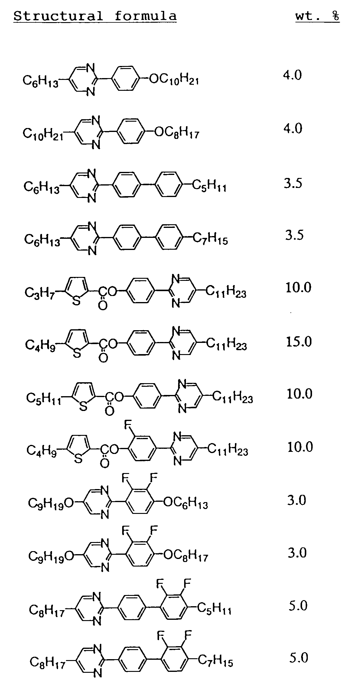
- a chiral smectic liquid crystal composition LC-1 was prepared by mixing the following compounds in the indicated proportions.
- a 1200 ⁇ -thick ITO film was formed as a transparent electrode, and thereon, a polyimide precursor ("SE-7992") was applied by spin coating and pre-dried at 80 °C for 5 min., followed by hot-curing at 200 °C for 1 hour to form 500 ⁇ -thick polyimide film.
- SE-7992 polyimide precursor
- Each of the thus-obtained polyimide film was subjected to rubbing treatment (as a uniaxial aligning treatment) with a nylon cloth under the following conditions to provide an alignment control layer.
- Rubbing roller a 10 cm-dia. roller about which a nylon cloth ("NF-77", mfd. by Teijin K.K.) was wound.
- the liquid crystal composition LC-1 was injected into each of the above-prepared blank cells in its cholesteric phase state and gradually cooled to a temperature providing chiral smectic C phase to prepare liquid crystal cells b-0 and b-1.
- each of the cells was subjected to a voltage application treatment such that a DC (offset) voltage of -2 volts was applied in a temperature range of Tc ⁇ 2 °C (Tc: Ch-SmC* phase transition temperature) while cooling each device at a rate of 1 °C/min.
- liquid crystal cells b-0 and b-1 were evaluated in the following manner in terms of alignment state and optical response characteristics, respectively.
- the alignment state of the liquid crystal composition LC-1 of each of the liquid crystal cells b-0 and b-1 was observed through a polarizing microscope at 30 °C (room temperature).
- Each of the liquid crystal cells b-0 and b-1 was set in a polarizing microscope equipped with a photomultiplier under cross nicol relationship so that a polarizing axis was disposed to provide the darkest state under no voltage application.
- each of the liquid crystal cells b-0 and b-1 provided a saturation tilt angle of 51.8 degrees (cone angle (54.8 degrees) - 3 degrees).
- each of the liquid crystal devices B-0 and B-1 was comprised of the above-prepared liquid crystal cell (b-0 or b-1) 52 (planar area: 0.9 cm 2 ), a single-crystalline silicon transistor 51 (ON-state resistance: 50 ohm), and a ceramic (storage) capacitor (capacitance: 2 nF).
- One of the liquid crystal devices was supplied with a gate (canning) signal voltage in a selection (gate-on) period of 30 ⁇ sec from a gate (scanning) signal line 23 and supplied with a prescribed data signal voltage Vop from a data signal line 25.
- the liquid crystal device B-1 was continuously supplied for 500 hours with a maximum of Vop of 6 volts providing a maximum tilt angle of 45 degrees, which was 87 % of the saturation tilt angle (51.8 degrees).
- the liquid crystal device B-0 was leftstanding for 500 hours under no voltage application.
- liquid crystal devices B-0 and B-1 were subjected to evaluation of V-T characteristic at 30 °C by using a triangular wave (0 - ⁇ 5 volts, 0.1 Hz).
- V-T curves for the liquid crystal device B-1 (solid line) and the liquid crystal device B-0 (dotted line) are shown in Figure 12.
- the two V-T curves for the liquid crystal devices B-0 and B-1 were close to each other and merely provided a maximum difference in transmittance of ca. 4.5 %.
- Two active matrix-type liquid crystal devices B-2 (for continuous voltage application) and B-0 (for continuous no voltage application) were prepared and evaluated in the same manner as in Example 3 except that the maximum Vop value (6 volts) was changed to 12 volts (for the device B-2) providing a maximum tilt angle of 51.8 degrees (100 % of the saturation tilt angle (51.8 degrees)).
Landscapes
- Engineering & Computer Science (AREA)
- Chemical & Material Sciences (AREA)
- Crystallography & Structural Chemistry (AREA)
- Physics & Mathematics (AREA)
- Computer Hardware Design (AREA)
- General Physics & Mathematics (AREA)
- Theoretical Computer Science (AREA)
- Liquid Crystal (AREA)
- Liquid Crystal Display Device Control (AREA)
- Control Of Indicators Other Than Cathode Ray Tubes (AREA)
Abstract
Description
a step of driving the liquid crystal device so that the liquid crystal is tilted from the monostable state to provide a maximum tilt angle in actual drive smaller than a saturation tilt angle.

- Cry:
- crystal phase,
- SmC*:
- chiral smectic C phase,
- Ch:
- cholesteric phase, and
- Iso:
- isotropic phase


Claims (9)
- A driving method for a liquid crystal device of the type comprising a pair of oppositely disposed substrates each provided with an electrode, a chiral smectic liquid crystal disposed between the substrates to form a plurality of pixels, and a plurality of active elements each of which is provided to an associated pixel and is connected with an associated electrode so as to effect a matrix drive of the liquid crystal device, the liquid crystal being placed in a monostable state under no voltage application; said method comprising:
a step of driving the liquid crystal device so that the liquid crystal is tilted from the monostable state to provide a maximum tilt angle in actual drive smaller than a saturation tilt angle. - A method according to Claim 1, wherein the maximum tilt angle is at most 95 % of the saturation tilt angle.
- A method according to Claim 1, wherein the maximum tilt angle is at most 90 % of the saturation tilt angle.
- A method according to Claim 1, wherein the maximum tilt angle is at most 80 % of the saturation tilt angle.
- A method according to any one of Claims 1 - 4, wherein the liquid crystal device provides a V-shaped voltage-transmittance curve being symmetrical with respect to an axis for representing a transmittance.
- A method according to any one of Claims 1 - 4, wherein the liquid crystal device provides a Half V-shaped voltage-transmittance curve being asymmetrical with respect to an axis for representing a transmittance.
- A method according to any one of Claims 1 - 4, wherein the saturation tilt angle is at least 45 degrees.
- A method according to Claim 5, wherein the saturation tilt angle is at least 45 degrees.
- A method according to claim 6, wherein the saturation tilt angle is at least 45 degrees.
Applications Claiming Priority (4)
| Application Number | Priority Date | Filing Date | Title |
|---|---|---|---|
| JP23767699 | 1999-08-25 | ||
| JP23767699 | 1999-08-25 | ||
| JP2000253308 | 2000-08-24 | ||
| JP2000253308A JP2001133751A (en) | 1999-08-25 | 2000-08-24 | Driving method of liquid crystal element |
Publications (2)
| Publication Number | Publication Date |
|---|---|
| EP1079363A2 true EP1079363A2 (en) | 2001-02-28 |
| EP1079363A3 EP1079363A3 (en) | 2002-03-27 |
Family
ID=26533314
Family Applications (1)
| Application Number | Title | Priority Date | Filing Date |
|---|---|---|---|
| EP00307292A Withdrawn EP1079363A3 (en) | 1999-08-25 | 2000-08-24 | Driving method for liquid crystal device |
Country Status (3)
| Country | Link |
|---|---|
| EP (1) | EP1079363A3 (en) |
| JP (1) | JP2001133751A (en) |
| KR (1) | KR100344366B1 (en) |
Cited By (3)
| Publication number | Priority date | Publication date | Assignee | Title |
|---|---|---|---|---|
| US6420000B1 (en) * | 1999-03-25 | 2002-07-16 | Canon Kabushiki Kaisha | Liquid crystal device and driving method for the device |
| KR100412491B1 (en) * | 2001-10-10 | 2003-12-31 | 삼성전자주식회사 | Reflective type ferroelectric liquid crystal display |
| KR100412489B1 (en) * | 2001-10-10 | 2003-12-31 | 삼성전자주식회사 | ferroelectric liquid crystal display |
Families Citing this family (1)
| Publication number | Priority date | Publication date | Assignee | Title |
|---|---|---|---|---|
| JP2008046651A (en) * | 2007-09-18 | 2008-02-28 | Fujitsu Ltd | Driving method of liquid crystal display device |
Family Cites Families (3)
| Publication number | Priority date | Publication date | Assignee | Title |
|---|---|---|---|---|
| US5920301A (en) * | 1994-06-10 | 1999-07-06 | Casio Computer Co., Ltd. | Liquid crystal display apparatus using liquid crystal having ferroelectric phase and method of driving liquid crystal display device using liquid crystal having ferroelectric phase |
| US5847799A (en) * | 1995-05-31 | 1998-12-08 | Casio Computer Co., Ltd. | Antiferroelectric liquid crystal display device |
| JPH10253994A (en) * | 1997-03-14 | 1998-09-25 | Toshiba Corp | Liquid crystal display |
-
2000
- 2000-08-24 EP EP00307292A patent/EP1079363A3/en not_active Withdrawn
- 2000-08-24 JP JP2000253308A patent/JP2001133751A/en active Pending
- 2000-08-25 KR KR1020000049463A patent/KR100344366B1/en not_active Expired - Fee Related
Cited By (3)
| Publication number | Priority date | Publication date | Assignee | Title |
|---|---|---|---|---|
| US6420000B1 (en) * | 1999-03-25 | 2002-07-16 | Canon Kabushiki Kaisha | Liquid crystal device and driving method for the device |
| KR100412491B1 (en) * | 2001-10-10 | 2003-12-31 | 삼성전자주식회사 | Reflective type ferroelectric liquid crystal display |
| KR100412489B1 (en) * | 2001-10-10 | 2003-12-31 | 삼성전자주식회사 | ferroelectric liquid crystal display |
Also Published As
| Publication number | Publication date |
|---|---|
| KR20010021414A (en) | 2001-03-15 |
| JP2001133751A (en) | 2001-05-18 |
| EP1079363A3 (en) | 2002-03-27 |
| KR100344366B1 (en) | 2002-07-24 |
Similar Documents
| Publication | Publication Date | Title |
|---|---|---|
| US6417828B1 (en) | Liquid crystal composition, liquid crystal device, driving method thereof and liquid crystal apparatus | |
| EP0811867A2 (en) | Liquid crystal display | |
| US6577289B1 (en) | Liquid crystal device and display apparatus including the device | |
| US6636193B1 (en) | Liquid crystal device | |
| US5999157A (en) | Suppressing liquid crystal movement based on the relationship between a display pattern and a driving waveform | |
| JP4790121B2 (en) | Monostable ferroelectric active matrix display | |
| EP1079363A2 (en) | Driving method for liquid crystal device | |
| KR100337771B1 (en) | Liquid crystal device | |
| US5956010A (en) | Liquid crystal apparatus and driving method | |
| JP4728479B2 (en) | Monostable ferroelectric active matrix display | |
| JP2000275683A (en) | Liquid crystal element and method for driving the liquid crystal element | |
| JPH09185061A (en) | Liquid crystal element and liquid crystal device | |
| JP3524406B2 (en) | Liquid crystal element | |
| JP3377190B2 (en) | Chiral smectic liquid crystal element, method of manufacturing the same, and liquid crystal device | |
| JP2003195359A (en) | Manufacturing method of liquid crystal element | |
| JP3530799B2 (en) | Manufacturing method and driving method of chiral smectic liquid crystal device | |
| JP3219709B2 (en) | Liquid crystal element, liquid crystal device, and method of driving liquid crystal element | |
| JP2000347160A (en) | Ferroelectric liquid crystal device | |
| JP2001215534A (en) | Liquid crystal element and method for driving the liquid crystal element | |
| JPH08152598A (en) | Liquid crystal device and driving method thereof | |
| JP2000330092A (en) | Liquid crystal device | |
| JP2000275685A (en) | Liquid crystal element and liquid crystal device having the same | |
| JPH0961827A (en) | Liquid crystal element, manufacturing method thereof, and liquid crystal device | |
| JP2000290652A (en) | Liquid crystal element and liquid crystal device having the same | |
| JP2000275618A (en) | Liquid crystal element and liquid crystal device having the same |
Legal Events
| Date | Code | Title | Description |
|---|---|---|---|
| PUAI | Public reference made under article 153(3) epc to a published international application that has entered the european phase |
Free format text: ORIGINAL CODE: 0009012 |
|
| AK | Designated contracting states |
Kind code of ref document: A2 Designated state(s): DE FR GB Kind code of ref document: A2 Designated state(s): AT BE CH CY DE DK ES FI FR GB GR IE IT LI LU MC NL PT SE |
|
| AX | Request for extension of the european patent |
Free format text: AL;LT;LV;MK;RO;SI |
|
| PUAL | Search report despatched |
Free format text: ORIGINAL CODE: 0009013 |
|
| AK | Designated contracting states |
Kind code of ref document: A3 Designated state(s): AT BE CH CY DE DK ES FI FR GB GR IE IT LI LU MC NL PT SE |
|
| AX | Request for extension of the european patent |
Free format text: AL;LT;LV;MK;RO;SI |
|
| 17P | Request for examination filed |
Effective date: 20020814 |
|
| AKX | Designation fees paid |
Free format text: DE FR GB |
|
| 17Q | First examination report despatched |
Effective date: 20040303 |
|
| STAA | Information on the status of an ep patent application or granted ep patent |
Free format text: STATUS: THE APPLICATION HAS BEEN WITHDRAWN |
|
| 18W | Application withdrawn |
Effective date: 20040714 |