EP1076447A2 - Circuit de filtre de blocage d' impédance - Google Patents
Circuit de filtre de blocage d' impédance Download PDFInfo
- Publication number
- EP1076447A2 EP1076447A2 EP00305893A EP00305893A EP1076447A2 EP 1076447 A2 EP1076447 A2 EP 1076447A2 EP 00305893 A EP00305893 A EP 00305893A EP 00305893 A EP00305893 A EP 00305893A EP 1076447 A2 EP1076447 A2 EP 1076447A2
- Authority
- EP
- European Patent Office
- Prior art keywords
- inductor
- end connected
- filter circuit
- circuit
- common point
- Prior art date
- Legal status (The legal status is an assumption and is not a legal conclusion. Google has not performed a legal analysis and makes no representation as to the accuracy of the status listed.)
- Ceased
Links
- 230000000903 blocking effect Effects 0.000 title claims abstract description 65
- 239000003990 capacitor Substances 0.000 claims abstract description 44
- 230000006855 networking Effects 0.000 claims abstract description 11
- 238000012937 correction Methods 0.000 claims abstract description 7
- 101150012579 ADSL gene Proteins 0.000 claims abstract 3
- 102100020775 Adenylosuccinate lyase Human genes 0.000 claims abstract 3
- 108700040193 Adenylosuccinate lyases Proteins 0.000 claims abstract 3
- 235000014676 Phragmites communis Nutrition 0.000 claims description 41
- 238000004804 winding Methods 0.000 claims description 38
- 230000001939 inductive effect Effects 0.000 claims description 8
- 230000009977 dual effect Effects 0.000 claims description 7
- 229910044991 metal oxide Inorganic materials 0.000 claims description 4
- 150000004706 metal oxides Chemical class 0.000 claims description 4
- 239000000654 additive Substances 0.000 abstract description 6
- 230000000996 additive effect Effects 0.000 abstract description 6
- 238000010586 diagram Methods 0.000 description 18
- 230000000694 effects Effects 0.000 description 7
- 230000001012 protector Effects 0.000 description 6
- 230000001965 increasing effect Effects 0.000 description 4
- 230000001052 transient effect Effects 0.000 description 4
- 230000002411 adverse Effects 0.000 description 3
- 238000012360 testing method Methods 0.000 description 3
- 230000008901 benefit Effects 0.000 description 2
- 230000005540 biological transmission Effects 0.000 description 2
- 238000013461 design Methods 0.000 description 2
- 230000006866 deterioration Effects 0.000 description 2
- 238000012986 modification Methods 0.000 description 2
- 230000004048 modification Effects 0.000 description 2
- 229910000859 α-Fe Inorganic materials 0.000 description 2
- 230000015556 catabolic process Effects 0.000 description 1
- 230000008859 change Effects 0.000 description 1
- 238000006243 chemical reaction Methods 0.000 description 1
- 238000006731 degradation reaction Methods 0.000 description 1
- 230000005669 field effect Effects 0.000 description 1
- 230000006872 improvement Effects 0.000 description 1
- 238000009434 installation Methods 0.000 description 1
- 238000004519 manufacturing process Methods 0.000 description 1
- 239000000463 material Substances 0.000 description 1
- 230000005405 multipole Effects 0.000 description 1
- 238000013021 overheating Methods 0.000 description 1
- 230000010363 phase shift Effects 0.000 description 1
- 230000002441 reversible effect Effects 0.000 description 1
- 238000012546 transfer Methods 0.000 description 1
Images


Classifications
-
- H—ELECTRICITY
- H03—ELECTRONIC CIRCUITRY
- H03H—IMPEDANCE NETWORKS, e.g. RESONANT CIRCUITS; RESONATORS
- H03H9/00—Networks comprising electromechanical or electro-acoustic devices; Electromechanical resonators
- H03H9/46—Filters
- H03H9/48—Coupling means therefor
- H03H9/52—Electric coupling means
-
- H—ELECTRICITY
- H03—ELECTRONIC CIRCUITRY
- H03G—CONTROL OF AMPLIFICATION
- H03G7/00—Volume compression or expansion in amplifiers
-
- H—ELECTRICITY
- H03—ELECTRONIC CIRCUITRY
- H03G—CONTROL OF AMPLIFICATION
- H03G11/00—Limiting amplitude; Limiting rate of change of amplitude ; Clipping in general
-
- H—ELECTRICITY
- H03—ELECTRONIC CIRCUITRY
- H03H—IMPEDANCE NETWORKS, e.g. RESONANT CIRCUITS; RESONATORS
- H03H7/00—Multiple-port networks comprising only passive electrical elements as network components
- H03H7/42—Networks for transforming balanced signals into unbalanced signals and vice versa, e.g. baluns
- H03H7/425—Balance-balance networks
- H03H7/427—Common-mode filters
-
- H—ELECTRICITY
- H04—ELECTRIC COMMUNICATION TECHNIQUE
- H04M—TELEPHONIC COMMUNICATION
- H04M11/00—Telephonic communication systems specially adapted for combination with other electrical systems
- H04M11/06—Simultaneous speech and data transmission, e.g. telegraphic transmission over the same conductors
- H04M11/062—Simultaneous speech and data transmission, e.g. telegraphic transmission over the same conductors using different frequency bands for speech and other data
-
- H—ELECTRICITY
- H03—ELECTRONIC CIRCUITRY
- H03H—IMPEDANCE NETWORKS, e.g. RESONANT CIRCUITS; RESONATORS
- H03H1/00—Constructional details of impedance networks whose electrical mode of operation is not specified or applicable to more than one type of network
- H03H2001/0021—Constructional details
- H03H2001/005—Wound, ring or feed-through type inductor
-
- H—ELECTRICITY
- H03—ELECTRONIC CIRCUITRY
- H03H—IMPEDANCE NETWORKS, e.g. RESONANT CIRCUITS; RESONATORS
- H03H7/00—Multiple-port networks comprising only passive electrical elements as network components
- H03H7/01—Frequency selective two-port networks
- H03H7/06—Frequency selective two-port networks including resistors
-
- H—ELECTRICITY
- H03—ELECTRONIC CIRCUITRY
- H03H—IMPEDANCE NETWORKS, e.g. RESONANT CIRCUITS; RESONATORS
- H03H7/00—Multiple-port networks comprising only passive electrical elements as network components
- H03H7/01—Frequency selective two-port networks
- H03H7/17—Structural details of sub-circuits of frequency selective networks
- H03H7/1741—Comprising typical LC combinations, irrespective of presence and location of additional resistors
- H03H7/1766—Parallel LC in series path
Definitions
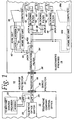
- the capacitor C1 also provides additional attenuation of the ADSL signals so as to prevent driving the telephone impedance into a non-linear region and converting the high frequency ADSL signals into audible signals which can be heard by the subscriber or converted to another ADSL band and cause ADSL interference. While there may still exist other minor resonances in the telephone set in the frequency range of between 20 KHz and 60 KHz, their undesirable effect is significantly reduced by the resistors R1 and R2 which produce a de-Q effect. It should be noted that the inductors L1 and L2 are formed as separate inductors so as to avoid longitudinal impedance problems as well as blocking differential impedances.
- FIG. 6 of the drawings there is shown a schematic circuit diagram of the current limiting protection circuitry 74 which is comprised of depletion mode N-channel field-effect transistors (FET) Q1, Q2; resistors R1a, R2a; and varistors RV1, RV2.
- the FET Q1 has its drain electrode connected to a first input terminal 76, its source electrode connected to one end of the resistor R1a, and its gate electrode connected to the other end of the resistor R1a.
- the common point C of the gate electrode of the transistor Q1 and the resistor R1a is also joined to the first output terminal 78.
- the transistors Q1, Q2 have a large tolerance on current limit and the resistors R1a, R2a permit the desired current limit value to be adjusted.
- the resistors R1a, R2a may have a value of zero Ohms or be entirely eliminated.
- the impedance filter circuit of the present invention adequately filters and blocks the telephone impedances from the home networking signals, which are in the frequency band of 5-10 MHz, it will be noted that the home networking signals from the telephone company's C.O. are however still connected to the house wiring via the NID/surge protector unit 32.
- the demarcation filter 84 includes two input (tip and ring) terminals 86, 88 which are connectable to the incoming lines via the jack side of the demarcation unit 36 in the NID/surge protector unit 32 and two output (tip and ring) terminals 90, 92 which are connectable to the internal house wiring via the plug side of the demarcation unit 36.
- the demarcation filter is comprised of six inductors L9-L14 and two capacitors C2, C3. In use, the demarcation filter is transparent to the ADSL data signals having the frequencies between 30 KHz and 2 MHz but will produce an attenuation of more than 40 dB for frequencies above 5 MHz. The demarcation filter will also provide an inductive input impedance for above 5 MHz frequency band so as to prevent loading down the home networking signals on the incoming phone lines and also adds data security benefits.
- the present invention provides an impedance blocking filter circuit used in telecommunication systems for interconnecting between incoming telephone lines and customer's terminal equipment so as to unconditionally block impedances above 20 KHz due to the customer's terminal equipment from an ADSL network interface unit and/or home networking interface unit.
- the impedance blocking filter circuit is comprised of six inductors, two resistors, and a capacitor.
- the shunt capacitance problem is caused by the added capacitance from all of the filter circuits connected to the on-hook phones.
- the return loss problem is due to the fact that the series inductances of the impedance blocking filter circuit connected to the telephone set going "off-hook" will cause a resonance to occur in the frequency range of 2-5 KHz with the total capacitance seen, which is equal to the sum of the line capacitance plus the capacitance from the filter circuits. Further, as the total capacitance is increased this will also cause a lower resonant frequency which will create a phase shift so to unbalance the telephone hybrid. As a result, the side tone level of the "off-hook" telephone set to increase.
- a second reed switch K2 and a capacitor C2 have been successively added to convert the third-order filter circuit to a fourth-order filter circuit which is optimized for better operation for fill rate ADSL modems.
- the reed switch K2 connected in series with the capacitor C2 is joined between common points C and D.
- a metal-oxide varistor D2 connected in series with the capacitor C2 and in parallel with the reed switch K2.
- the varistor D2 is used to protect the capacitor C2 from being destroyed by transients when the telephone set is in the on-hook condition.
- thermo-fuse F1 may be optionally connected in series the inductors L5, L3, L1, L7, L9 and the tank circuit TC1 which are arranged between the input tip terminal 66 and the output tip terminal 70.
- the thermo-fuse F1 may be electrically interconnected between the input tip terminal 68 and the inductor L5.
- the thermo-fuse F1 is located physically adjacent to on e the inductors or the resistor in order to sense the highest temperature within the filter circuit.
- the fuse F1 provides a safety feature and will open when the sensed temperature of the filter circuit exceed a specified trip temperature.
- the fuse functions as a safety protection means for preventing the filter circuit from overheating and causing a fire due to a power cross on the phone lines.
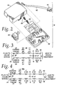
- inductor device T1 includes a cylindrical-shaped housing 110 which contains the first winding inductor W1 of the first tank circuit TC1, the second winding inductor W2 of the second tank circuit TC2, the reed switch K1, and the reed switch K2.
- FIG 11(a) there is depicted a top plan view of a current sensor unit CS for use in the filter circuits of Figures 8 and 9.
- Figure 11(b) is a side elevational view of the current sensor unit CS.
- the current sensor unit CS is formed of cylindrical housing 112 and contains a single inductor L and a single reed switch K. It should be apparent to those skilled in the art that the dual winding inductor device T1 can be replaced with two such current sensor units CS so as to render the same operation. Since the windings W1,W2 or the inductor L is used the reed switches K1,K2 (K), the reed switch is selected to be actuatable on a loop current threshold of approximately 14-20 mA.
- the reed switch may chatter during ringing on a 1 REN telephone and may thus shorten the useful life of the reed switch.
- the loop current threshold is above 20 mA, then the amount of loop current may be insufficient to be actuable in the worst case condition (e.g., the longest cable).
- FIG 12 there is illustrated a fifth embodiment of an impedance blocking filter circuit 59d of the present invention, the fifth embodiment is substantially identical to the first embodiment of the second-order filter circuit of Figure 3, except that the resistors R1 and R2 have been eliminated and a reed switch K1 has been added in series with the capacitor C1 located between the common points A and B. Further, the four single inductors L1, L2 and L3, L4 of Figure 3 have replace by a multi-sectioned bobbins structure T2.
- the bobbin structure T2 includes a tip winding TW (corresponding to inductors L1,L2) connected between the inductor L5 and the common point A , and a ring winding RW (corresponding to inductors L3,L4) connected between the inductor L6 and the common point B. Further, the bobbin structure T2 houses the reed switches K1,K2.
- the tip(ring) winding TW(RW) combines the inductor L1(L2) for the ADSL frequency band (30KHz to 2MHz) and the inductor L3(L4) for the mid-frequency band (1MHz to 20MHz) into a single coil.
- a return loss correction circuit consisting of a first tank circuit TC1 and a second tank circuit TC2 may be interconnected between the common points A,B and the output terminals 70,72.
- FIG 13 there is shown a sixth embodiment of an impedance filter circuit 59e of the present invention, the sixth embodiment includes all of the circuit components of the filter circuit 59d of Figure 12 and has added an inductor L7 and an inductor L8.
- the inductor L7 is interconnected between the common point A and the output tip terminal 70
- the inductor L8 is interconnected between the common point B and the output ring terminal 72.
- the filter circuit thus far described is essentially a third-order filter circuit for producing a better stop band.
- FIG 14(a) there is shown a side view of a wiring bobbin structure T2 having multiple sections S1-S4 for use in the circuits of Figures 12 and 13.
- Figure 14(b) is schematic diagram of the bobbin structure T2 of Figure 14(a).
- the bobbin structure includes a first narrow section S1 on which is wound the inductor L3, a first wider section S2 on which is wound the inductor L1, a second narrow section S3 on which is wound the inductor L4, and a second wider section S4 on which is wound the inductor L2.
- the inductors L1,L3 are combined on the same coil and is represented by the tip winding TW in Figure 14(b).
- the inductors L2,L4 are combined on the coil and is represented by the ring winding RW.
Landscapes
- Engineering & Computer Science (AREA)
- Computer Networks & Wireless Communication (AREA)
- Signal Processing (AREA)
- Physics & Mathematics (AREA)
- Acoustics & Sound (AREA)
- Filters And Equalizers (AREA)
- Telephonic Communication Services (AREA)
- Networks Using Active Elements (AREA)
Applications Claiming Priority (2)
| Application Number | Priority Date | Filing Date | Title |
|---|---|---|---|
| US370137 | 1995-01-09 | ||
| US09/370,137 US6181777B1 (en) | 1998-11-19 | 1999-08-09 | Impedance blocking filter circuit |
Publications (2)
| Publication Number | Publication Date |
|---|---|
| EP1076447A2 true EP1076447A2 (fr) | 2001-02-14 |
| EP1076447A3 EP1076447A3 (fr) | 2004-06-23 |
Family
ID=23458386
Family Applications (1)
| Application Number | Title | Priority Date | Filing Date |
|---|---|---|---|
| EP00305893A Ceased EP1076447A3 (fr) | 1999-08-09 | 2000-07-12 | Circuit de filtre de blocage d' impédance |
Country Status (7)
| Country | Link |
|---|---|
| US (2) | US6181777B1 (fr) |
| EP (1) | EP1076447A3 (fr) |
| KR (1) | KR20010021156A (fr) |
| CN (2) | CN1201551C (fr) |
| AU (1) | AU763423B2 (fr) |
| CA (1) | CA2314052C (fr) |
| SG (1) | SG86423A1 (fr) |
Cited By (4)
| Publication number | Priority date | Publication date | Assignee | Title |
|---|---|---|---|---|
| EP1168803A2 (fr) * | 2000-06-19 | 2002-01-02 | Broadcom HomeNetworking, Inc. | Procédé et dispositif pour couplage d'un circuit de modem à frequence vocale à un connecteur de téléphone commun |
| WO2003045043A1 (fr) * | 2001-11-14 | 2003-05-30 | Excelsus Technologies, Inc. | Appareil de micro-filtre et de separateur haute performance |
| AU2005200624B2 (en) * | 2001-11-14 | 2007-08-02 | Pulse Engineering, Inc. | High performance micro-filter and splitter apparatus |
| EP1901538A1 (fr) * | 2006-09-13 | 2008-03-19 | Ycl Electronics Co., Ltd. | Séparateur de signal |
Families Citing this family (43)
| Publication number | Priority date | Publication date | Assignee | Title |
|---|---|---|---|---|
| US6711260B1 (en) * | 1998-08-18 | 2004-03-23 | Sbc Technology Resources, Inc. | Method and apparatus for spectral containment over telephone service lines |
| US6813343B1 (en) | 1999-05-12 | 2004-11-02 | Orckitt Communications Ltd. | Method and apparatus for filtering asymmetric digital subscriber line (ADSL) signals |
| US6459790B1 (en) * | 1999-08-27 | 2002-10-01 | Efficient Networks, Inc. | System and method for selective filter isolation |
| WO2002005451A1 (fr) * | 2000-07-11 | 2002-01-17 | Inari, Inc. | Adaptateur de reseau de ligne electrique modulaire |
| AU2001227339A1 (en) * | 2000-10-13 | 2002-05-15 | Sharegate Inc. | Method and device for mitigating the effects of quarter-wave shorts caused by branched wiring |
| US6978011B1 (en) * | 2001-03-02 | 2005-12-20 | Alcatel | Enhanced low pass filter |
| US20030058840A1 (en) * | 2001-03-08 | 2003-03-27 | Doose Nathan G. | In-line filter for combined telecommunication applications |
| US7110931B2 (en) * | 2001-03-12 | 2006-09-19 | Pulse Engineering, Inc. | Advanced electronic signal conditioning assembly and method |
| US7174147B2 (en) * | 2001-04-11 | 2007-02-06 | Kyocera Wireless Corp. | Bandpass filter with tunable resonator |
| US7746292B2 (en) * | 2001-04-11 | 2010-06-29 | Kyocera Wireless Corp. | Reconfigurable radiation desensitivity bracket systems and methods |
| US7154440B2 (en) * | 2001-04-11 | 2006-12-26 | Kyocera Wireless Corp. | Phase array antenna using a constant-gain phase shifter |
| US6690251B2 (en) * | 2001-04-11 | 2004-02-10 | Kyocera Wireless Corporation | Tunable ferro-electric filter |
| US7394430B2 (en) * | 2001-04-11 | 2008-07-01 | Kyocera Wireless Corp. | Wireless device reconfigurable radiation desensitivity bracket systems and methods |
| US7221243B2 (en) * | 2001-04-11 | 2007-05-22 | Kyocera Wireless Corp. | Apparatus and method for combining electrical signals |
| US7164329B2 (en) | 2001-04-11 | 2007-01-16 | Kyocera Wireless Corp. | Tunable phase shifer with a control signal generator responsive to DC offset in a mixed signal |
| US7099302B2 (en) * | 2001-04-25 | 2006-08-29 | Infineon Technologies Ag | Data transmission network |
| EP1287674B1 (fr) * | 2001-04-25 | 2010-02-24 | Infineon Technologies AG | Reseau d'emission de donnees |
| US6757380B2 (en) | 2001-07-13 | 2004-06-29 | Csi/Suttle Apparatus Corporation | Impedance blocking filter circuit for digital subscriber line communication systems |
| US7071776B2 (en) | 2001-10-22 | 2006-07-04 | Kyocera Wireless Corp. | Systems and methods for controlling output power in a communication device |
| US7057486B2 (en) * | 2001-11-14 | 2006-06-06 | Pulse Engineering, Inc. | Controlled induction device and method of manufacturing |
| US7180467B2 (en) * | 2002-02-12 | 2007-02-20 | Kyocera Wireless Corp. | System and method for dual-band antenna matching |
| US7184727B2 (en) * | 2002-02-12 | 2007-02-27 | Kyocera Wireless Corp. | Full-duplex antenna system and method |
| US7176845B2 (en) * | 2002-02-12 | 2007-02-13 | Kyocera Wireless Corp. | System and method for impedance matching an antenna to sub-bands in a communication band |
| US7206322B1 (en) * | 2002-03-11 | 2007-04-17 | At&T Corp. | System and method for using ADSL for introducing multiple derived lines over a single line |
| AU2003261267A1 (en) * | 2002-07-25 | 2004-02-16 | Pulse Engineering, Inc. | High density electronics assembly and method |
| US7109837B2 (en) * | 2003-03-18 | 2006-09-19 | Pulse Engineering, Inc. | Controlled inductance device and method |
| US20050088267A1 (en) * | 2002-09-17 | 2005-04-28 | Charles Watts | Controlled inductance device and method |
| US7009482B2 (en) | 2002-09-17 | 2006-03-07 | Pulse Engineering, Inc. | Controlled inductance device and method |
| US7136270B2 (en) * | 2003-01-28 | 2006-11-14 | Gateway Inc. | Surge protector including data pass-through |
| US7720443B2 (en) | 2003-06-02 | 2010-05-18 | Kyocera Wireless Corp. | System and method for filtering time division multiple access telephone communications |
| US8763063B2 (en) * | 2004-06-01 | 2014-06-24 | Time Warner Cable Enterprises Llc | Controlled isolation splitter apparatus and methods |
| US8095098B2 (en) * | 2004-06-01 | 2012-01-10 | Time Warner Cable Inc. | Apparatus and methods for network interface and spectrum management |
| US7248845B2 (en) * | 2004-07-09 | 2007-07-24 | Kyocera Wireless Corp. | Variable-loss transmitter and method of operation |
| JP4483552B2 (ja) * | 2004-11-30 | 2010-06-16 | Tdk株式会社 | サージ吸収回路 |
| JP4135711B2 (ja) * | 2004-12-17 | 2008-08-20 | 株式会社デンソー | 視認力向上支援装置 |
| US7548762B2 (en) * | 2005-11-30 | 2009-06-16 | Kyocera Corporation | Method for tuning a GPS antenna matching network |
| WO2007082345A1 (fr) * | 2006-01-18 | 2007-07-26 | Advanced Circuits And Systems Pty Ltd | Filtre et circuit de commutation |
| AU2006100490B4 (en) * | 2006-01-18 | 2006-12-21 | Advanced Circuits And Systems Pty Ltd | A filter |
| EP1827055A1 (fr) * | 2006-02-27 | 2007-08-29 | Thomson Telecom Belgium | Dispositif fournissant des services téléphoniques aux téléphones enfichés sur un câble téléphonique résidentiel qui n'est pas connecté à un central téléphonique |
| US8625704B1 (en) * | 2008-09-25 | 2014-01-07 | Aquantia Corporation | Rejecting RF interference in communication systems |
| CN102025837A (zh) * | 2009-09-17 | 2011-04-20 | 鸿富锦精密工业(深圳)有限公司 | 网间连接器及检测电话拨号连接的方法 |
| GB2501532A (en) * | 2012-04-26 | 2013-10-30 | Ibm | Bounding a metric for data mining on compressed data vectors |
| WO2018056148A1 (fr) * | 2016-09-26 | 2018-03-29 | 株式会社村田製作所 | Dispositif de filtre à ondes acoustiques, circuit frontal à haute fréquence, et dispositif de communication |
Citations (4)
| Publication number | Priority date | Publication date | Assignee | Title |
|---|---|---|---|---|
| EP0677938A1 (fr) * | 1994-04-14 | 1995-10-18 | ALCATEL BELL Naamloze Vennootschap | Dispositif de couplage de signaux |
| WO1998027713A1 (fr) * | 1996-12-17 | 1998-06-25 | Paradyne Corporation | Systeme de filtres passifs repartis et procede correspondant |
| US5802170A (en) * | 1994-05-19 | 1998-09-01 | Tii Industries, Inc. | Customer bridge module |
| EP0923221A1 (fr) * | 1997-12-09 | 1999-06-16 | Nortel Networks Corporation | Séparateur et filtre de signaux de communication |
Family Cites Families (18)
| Publication number | Priority date | Publication date | Assignee | Title |
|---|---|---|---|---|
| US4613732A (en) * | 1983-10-24 | 1986-09-23 | Northern Telecom Limited | Interface module with modular jack for telecommunications systems |
| US4742541A (en) * | 1983-10-25 | 1988-05-03 | Northern Telecom Limited | Telecommunications interface with protector modules |
| US4667173A (en) * | 1985-08-29 | 1987-05-19 | Kabushiki Kaisha Toshiba | Line filter |
| FR2606946A1 (fr) * | 1986-11-17 | 1988-05-20 | Telephonie Ind Commerciale | Dispositif de protection d'un equipement terminal chez un abonne telephonique |
| US4761623A (en) * | 1986-12-04 | 1988-08-02 | Corcom Inc. | Broadband RFI power line filter |
| US4743999A (en) * | 1987-02-13 | 1988-05-10 | Curtis Manufacturing Company, Inc. | Rotary telephone line surge protector and system |
| US5025443A (en) * | 1988-02-24 | 1991-06-18 | Integrated Network Corporation | Digital data over voice communication |
| US5077630A (en) * | 1990-03-28 | 1991-12-31 | Delta Design And Development Co. | Integrated services digital network terminating resistor with line fault protector |
| US5426698A (en) * | 1993-05-11 | 1995-06-20 | General Datacomm, Inc. | Transformed current sensing relay for use in switched network modems and circuit incorporating same |
| DE69417950T2 (de) * | 1993-05-26 | 1999-09-23 | Nippon Telegraph & Telephone | Filter zur Erzielung der elektromagnetischen Kompatibilität für eine symmetrische mehradrige Fernmeldeleitung |
| US5623543A (en) * | 1994-02-01 | 1997-04-22 | British Telecommunications Public Limited Company | Two port signalling voltages filter arrangement |
| US5642416A (en) * | 1995-03-03 | 1997-06-24 | Harris Corporation | AM broadcast band interference filter for line-powered telephone |
| US5848150A (en) * | 1997-02-26 | 1998-12-08 | Paradyne Corporation | Passive distributed filter system and method |
| US5930340A (en) * | 1997-07-07 | 1999-07-27 | Advanced Micro Devices | Device and method for isolating voice and data signals on a common carrier |
| US6144735A (en) * | 1998-03-12 | 2000-11-07 | Westell Technologies, Inc. | Filters for a digital subscriber line system for voice communication over a telephone line |
| US6137866A (en) * | 1998-05-28 | 2000-10-24 | Siecor Operations, Llc | Indoor XDSL splitter assembly |
| US6317464B1 (en) * | 1998-06-09 | 2001-11-13 | Nortel Networks Limited | Method and apparatus for separating digital data signals from analog voice signals transported over a common conductor |
| US6141377A (en) * | 1998-07-30 | 2000-10-31 | Cisco Technology, Inc. | Method and apparatus for voice frequency noise reduction in splitterless ADSL |
-
1999
- 1999-08-09 US US09/370,137 patent/US6181777B1/en not_active Ceased
-
2000
- 2000-07-12 EP EP00305893A patent/EP1076447A3/fr not_active Ceased
- 2000-07-13 AU AU47193/00A patent/AU763423B2/en not_active Ceased
- 2000-07-19 CA CA002314052A patent/CA2314052C/fr not_active Expired - Fee Related
- 2000-07-20 SG SG200004079A patent/SG86423A1/en unknown
- 2000-07-31 KR KR1020000044141A patent/KR20010021156A/ko active IP Right Grant
- 2000-08-09 CN CNB001227904A patent/CN1201551C/zh not_active Expired - Fee Related
- 2000-08-09 CN CN2005100080952A patent/CN1658499B/zh not_active Expired - Fee Related
-
2003
- 2003-01-30 US US10/355,897 patent/USRE39432E1/en not_active Expired - Fee Related
Patent Citations (4)
| Publication number | Priority date | Publication date | Assignee | Title |
|---|---|---|---|---|
| EP0677938A1 (fr) * | 1994-04-14 | 1995-10-18 | ALCATEL BELL Naamloze Vennootschap | Dispositif de couplage de signaux |
| US5802170A (en) * | 1994-05-19 | 1998-09-01 | Tii Industries, Inc. | Customer bridge module |
| WO1998027713A1 (fr) * | 1996-12-17 | 1998-06-25 | Paradyne Corporation | Systeme de filtres passifs repartis et procede correspondant |
| EP0923221A1 (fr) * | 1997-12-09 | 1999-06-16 | Nortel Networks Corporation | Séparateur et filtre de signaux de communication |
Cited By (7)
| Publication number | Priority date | Publication date | Assignee | Title |
|---|---|---|---|---|
| EP1168803A2 (fr) * | 2000-06-19 | 2002-01-02 | Broadcom HomeNetworking, Inc. | Procédé et dispositif pour couplage d'un circuit de modem à frequence vocale à un connecteur de téléphone commun |
| EP1168803A3 (fr) * | 2000-06-19 | 2008-08-13 | Broadcom Corporation | Procédé et dispositif pour couplage d'un circuit de modem à frequence vocale à un connecteur de téléphone commun |
| WO2003045043A1 (fr) * | 2001-11-14 | 2003-05-30 | Excelsus Technologies, Inc. | Appareil de micro-filtre et de separateur haute performance |
| AU2002249788B2 (en) * | 2001-11-14 | 2004-11-11 | Pulse Engineering, Inc. | High performance micro-filter and splitter apparatus |
| AU2005200624B2 (en) * | 2001-11-14 | 2007-08-02 | Pulse Engineering, Inc. | High performance micro-filter and splitter apparatus |
| EP1729472A3 (fr) * | 2001-11-14 | 2008-03-05 | Pulse Engineering, Inc. | Appareil pour conditionner et séparer des signaux de télécommunication |
| EP1901538A1 (fr) * | 2006-09-13 | 2008-03-19 | Ycl Electronics Co., Ltd. | Séparateur de signal |
Also Published As
| Publication number | Publication date |
|---|---|
| EP1076447A3 (fr) | 2004-06-23 |
| SG86423A1 (en) | 2002-02-19 |
| CA2314052A1 (fr) | 2001-02-09 |
| USRE39432E1 (en) | 2006-12-19 |
| AU763423B2 (en) | 2003-07-24 |
| US6181777B1 (en) | 2001-01-30 |
| CN1283920A (zh) | 2001-02-14 |
| CN1201551C (zh) | 2005-05-11 |
| CA2314052C (fr) | 2007-01-30 |
| CN1658499B (zh) | 2013-11-06 |
| CN1658499A (zh) | 2005-08-24 |
| AU4719300A (en) | 2001-02-15 |
| KR20010021156A (ko) | 2001-03-15 |
Similar Documents
| Publication | Publication Date | Title |
|---|---|---|
| AU763423B2 (en) | Impedance blocking filter circuit | |
| EP1128651B1 (fr) | Circuit de filtre de blocage d' impédance | |
| USRE44094E1 (en) | Impedance blocking filter circuit | |
| US6137880A (en) | Passive splitter filter for digital subscriber line voice communication for complex impedance terminations | |
| US7457405B2 (en) | Enhanced low pass filter | |
| AU746279B2 (en) | Filter arrangement | |
| US6757380B2 (en) | Impedance blocking filter circuit for digital subscriber line communication systems | |
| AU2002249788B2 (en) | High performance micro-filter and splitter apparatus | |
| US6483914B1 (en) | Telephone filter arrangement | |
| EP1248444A1 (fr) | Appareil téléphonique de test analogue possedant un filtre passe-bas et des resistances couplées avec les lignes de connection pour prévenir l'alteration des signaux de communication numériques | |
| TW480865B (en) | Cross-reference to related applications | |
| US20020027984A1 (en) | Filter | |
| AU2005200624B2 (en) | High performance micro-filter and splitter apparatus | |
| US20030058840A1 (en) | In-line filter for combined telecommunication applications | |
| TW474085B (en) | Impedance blocking filter circuit | |
| WO2001006737A1 (fr) | Filtre passe-bas d'ordre impair de dispositif pots | |
| US20030190039A1 (en) | Saturable core POTS/DSL filter | |
| US20020141570A1 (en) | Low-pass filter usable with caller ID device | |
| AU2006100159A4 (en) | A filter |
Legal Events
| Date | Code | Title | Description |
|---|---|---|---|
| PUAI | Public reference made under article 153(3) epc to a published international application that has entered the european phase |
Free format text: ORIGINAL CODE: 0009012 |
|
| AK | Designated contracting states |
Kind code of ref document: A2 Designated state(s): AT BE CH CY DE DK ES FI FR GB GR IE IT LI LU MC NL PT SE |
|
| AX | Request for extension of the european patent |
Free format text: AL;LT;LV;MK;RO;SI |
|
| 17P | Request for examination filed |
Effective date: 20040114 |
|
| PUAL | Search report despatched |
Free format text: ORIGINAL CODE: 0009013 |
|
| AK | Designated contracting states |
Kind code of ref document: A3 Designated state(s): AT BE CH CY DE DK ES FI FR GB GR IE IT LI LU MC NL PT SE |
|
| AX | Request for extension of the european patent |
Extension state: AL LT LV MK RO SI |
|
| RIC1 | Information provided on ipc code assigned before grant |
Ipc: 7H 03H 7/06 B Ipc: 7H 03H 7/01 B Ipc: 7H 04M 11/06 A |
|
| 17Q | First examination report despatched |
Effective date: 20040825 |
|
| RAP1 | Party data changed (applicant data changed or rights of an application transferred) |
Owner name: PULSE ENGINEERING, INC. |
|
| AKX | Designation fees paid |
Designated state(s): AT BE CH CY DE DK ES FI FR GB GR IE IT LI LU MC NL PT SE |
|
| STAA | Information on the status of an ep patent application or granted ep patent |
Free format text: STATUS: THE APPLICATION HAS BEEN REFUSED |
|
| 18R | Application refused |
Effective date: 20071201 |
|
| REG | Reference to a national code |
Ref country code: HK Ref legal event code: WD Ref document number: 1034626 Country of ref document: HK |