EP1076345A2 - Variable inductance element - Google Patents
Variable inductance element Download PDFInfo
- Publication number
- EP1076345A2 EP1076345A2 EP00402278A EP00402278A EP1076345A2 EP 1076345 A2 EP1076345 A2 EP 1076345A2 EP 00402278 A EP00402278 A EP 00402278A EP 00402278 A EP00402278 A EP 00402278A EP 1076345 A2 EP1076345 A2 EP 1076345A2
- Authority
- EP
- European Patent Office
- Prior art keywords
- pattern
- inductance element
- trimming
- variable inductance
- inductor pattern
- Prior art date
- Legal status (The legal status is an assumption and is not a legal conclusion. Google has not performed a legal analysis and makes no representation as to the accuracy of the status listed.)
- Withdrawn
Links
Images


Classifications
-
- H—ELECTRICITY
- H01—ELECTRIC ELEMENTS
- H01F—MAGNETS; INDUCTANCES; TRANSFORMERS; SELECTION OF MATERIALS FOR THEIR MAGNETIC PROPERTIES
- H01F38/00—Adaptations of transformers or inductances for specific applications or functions
- H01F38/08—High-leakage transformers or inductances
-
- H—ELECTRICITY
- H01—ELECTRIC ELEMENTS
- H01F—MAGNETS; INDUCTANCES; TRANSFORMERS; SELECTION OF MATERIALS FOR THEIR MAGNETIC PROPERTIES
- H01F17/00—Fixed inductances of the signal type
- H01F17/0006—Printed inductances
-
- H—ELECTRICITY
- H01—ELECTRIC ELEMENTS
- H01F—MAGNETS; INDUCTANCES; TRANSFORMERS; SELECTION OF MATERIALS FOR THEIR MAGNETIC PROPERTIES
- H01F41/00—Apparatus or processes specially adapted for manufacturing or assembling magnets, inductances or transformers; Apparatus or processes specially adapted for manufacturing materials characterised by their magnetic properties
- H01F41/02—Apparatus or processes specially adapted for manufacturing or assembling magnets, inductances or transformers; Apparatus or processes specially adapted for manufacturing materials characterised by their magnetic properties for manufacturing cores, coils, or magnets
- H01F41/04—Apparatus or processes specially adapted for manufacturing or assembling magnets, inductances or transformers; Apparatus or processes specially adapted for manufacturing materials characterised by their magnetic properties for manufacturing cores, coils, or magnets for manufacturing coils
- H01F41/041—Printed circuit coils
- H01F41/045—Trimming
-
- H—ELECTRICITY
- H01—ELECTRIC ELEMENTS
- H01F—MAGNETS; INDUCTANCES; TRANSFORMERS; SELECTION OF MATERIALS FOR THEIR MAGNETIC PROPERTIES
- H01F17/00—Fixed inductances of the signal type
- H01F17/0006—Printed inductances
- H01F2017/0073—Printed inductances with a special conductive pattern, e.g. flat spiral
-
- H—ELECTRICITY
- H01—ELECTRIC ELEMENTS
- H01F—MAGNETS; INDUCTANCES; TRANSFORMERS; SELECTION OF MATERIALS FOR THEIR MAGNETIC PROPERTIES
- H01F21/00—Variable inductances or transformers of the signal type
- H01F21/12—Variable inductances or transformers of the signal type discontinuously variable, e.g. tapped
- H01F2021/125—Printed variable inductor with taps, e.g. for VCO
-
- H—ELECTRICITY
- H01—ELECTRIC ELEMENTS
- H01F—MAGNETS; INDUCTANCES; TRANSFORMERS; SELECTION OF MATERIALS FOR THEIR MAGNETIC PROPERTIES
- H01F21/00—Variable inductances or transformers of the signal type
Definitions
- the present invention relates to a variable inductance element, and more particularly to a variable inductance element especially for use in a mobile communications device such as a mobile telephone or the like.
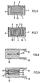
- FIG. 8 shows an example of such a conventional type of fine adjustment method.
- a trimming area 34 to function as an inductance element is formed between signal patterns 31 and 32.
- the trimming area 34 is irradiated with a laser beam emitted from a laser trimming machine (not shown) while the beam is linearly moved.
- the trimming area 34 is partially removed corresponding to the movement track of the laser beam, so that a linear trimming groove 35 is formed. Accordingly, the area of the trimming area 34 is changed so that the inductance of the trimming area 34 is finely adjusted.
- the trimming area 34 is made to have a large area.
- the groove width (trimming width) of the trimming groove 35 formed by one pass of the trimming laser is generally thin. For this reason, in the case where a wide trimming width is required, irradiation with a laser beam must be repeated while the irradiation position is moved in parallel, as shown in FIG. 9. Hence, there arises the problem that it takes much time to carry out the fine adjustment.
- variable inductance element having a high Q factor, and in which the inductance can be finely adjusted efficiently.
- variable inductance element which comprises (a) an insulating substrate, and (b) a substantially meandering inductor pattern defined by trimming a conductor provided on the surface of the insulating substrate such that predetermined island-shaped sections are separated from the inductor pattern.
- the width and the number of meanders of the inductor pattern are changed, causing the inductance to change.
- the pattern width of the substantially meandering inductor pattern at a substantially constant value, and setting the distance between neighboring portions of the substantially meandering inductor pattern to be at least two times as long as the pattern width of the inductor pattern, the distance between magnetic fields generated in the respective neighboring portions is large, and the magnetic fields can be prevented from interfering with each other.
- variable inductance element of the present invention will be described with reference to Figs.1 to 7 of the accompanying drawings.
- a conductor pattern 2 having a wide area is formed on the upper face of the insulating substrate 1 by a thick-film printing method or a thin-film forming method such as photolithography or the like.
- a thick-film printing method a mask having an opening in a desired pattern is made to cover the upper surface of the insulating substrate 1, and electrically conductive paste is coated from above the mask, whereby a conductor having a relatively large thickness is formed in the desired pattern (in the case of the first embodiment, the conductor pattern 2) on the upper surface of the insulating substrate 1 exposed through the opening of the mask.
- a relatively thin conductive film is formed on substantially the whole upper surface of the insulating substrate 1.
- a resist film for example, a photosensitive resin or the like
- a mask film having a predetermined image pattern is placed to cover the upper surface of the resist film, and the desired part of the resist film is hardened by irradiation of UV rays or the like.
- the resist film is removed, with the hardened part thereof remaining, and the exposed part of the conductive film is removed, whereby a conductor is formed in the desired pattern, and thereafter, the hardened resist film is also removed.
- photosensitive conductive paste may be coated onto the upper surface of the insulating substrate 1, and a mask film having a predetermined image pattern formed therein covers the photosensitive conductive paste, followed by exposure and development.
- the conductive pattern 2 is provided on substantially the whole of the insulating substrate 1.
- One end 2a of the conductor pattern 2 is led out to the rear portion of the left-side, as viewed in FIGS. 1, 2 and 3, of the insulating substrate 1, while the other end 2b is led out to the front portion of the right-side, as viewed in FIGS. 1, 2 and 3, of the insulation substrate 1.
- the insulating substrate glass, glass ceramic, alumina, ferrite, or other suitable material may be used.
- materials for the conductor pattern 2 Ag, Ag-Pd, Cu, Au, Ni, Al, or other suitable material may be employed.
- a liquid insulating material (polyimide or the like) is coated onto the whole of the upper surface of the insulating substrate 1 by spin coating, printing or the like, and is dried, whereby an insulating protection film (not shown) covering the conductor pattern 2 is formed.
- external input-output electrodes 6 and 7 are provided on each end portion of the insulating substrate 1 in the longitudinal direction, respectively.
- the external input-output electrode 6 is electrically connected to the end portion 2a of the conductor pattern 2
- the external input-output electrode 7 is electrically connected to the end portion 2b of the conductor pattern 2.
- the external input-output electrodes 6 and 7 are formed by coating and baking conductive paste of Ag, Ag-Pd, Cu, Ni, NiCr, NiCu, or other suitable material, by dry or wet plating, or by a combination of the coating and baking, and the plating.
- variable inductance element 9 obtained as described above is mounted onto a printed circuit board or the like, and the conductor pattern 2 is trimmed.
- the upper surface of the variable inductance element 9 is irradiated with a pulsed laser beam L while the beam L is being moved, so that U-shaped trimming grooves 10 are formed in the variable inductance element 9.
- the two trimming grooves 10 separate two island-shaped rectangular sections 3 from the conductor pattern 2 to form a meandering inductor pattern 4, as shown in FIG. 3.
- the ends 2a and 2b of the meandering inductor pattern 4 are electrically connected to the external input-output electrodes 6 and 7, respectively.
- the inductance element 9 can be provided with a Q factor required for a high frequency circuit.
- the U-shaped trimming grooves 10 in the conductor pattern 2 so as to form the meandering inductor pattern 4
- adjustment of the inductance is possible over a wider range as compared with that by the conventional linear trimming.
- the adjustment is possible only over a range of about 0.15 nH by conventional linear trimming.
- the adjustment range is about 1.0 nH (a range about 6.7 times as wide as that of the conventional trimming method).
- the pattern width V of a portion of the inductor pattern 4 extending in parallel to the width direction of the insulating substrate 1 is equal to the pattern width H of a portion thereof extending in parallel to the longitudinal direction of the insulation substrate 1, and the distance D between the leg portions of each U-shaped trimming groove 10 is set to be at least two times as long as the pattern width V (or the pattern width H).
- the pattern width of the inductor pattern 4 is substantially constant over the whole length thereof.
- the distance between neighboring portions of the inductor pattern 4 is at least two times as long as the pattern width.
- the Q factor of the inductance element 9 can be further enhanced. Concretely, the Q factor can be enhanced by about 40% as compared with that of a conventional variable inductance element.
- Trimming of the conductor pattern 2 is not restricted to a method using a laser beam, and may be carried out by any method such as sand blasting or the like. Further, it is not necessary to provide the trimming grooves 10. Provided that the conductor pattern 2 is electrically cut, the trimming grooves 10 do not have to be formed in a physical sense.
- a conductor pattern 22 is directly formed on a printed circuit board 21.
- the conductor pattern 22 which functions as an inductance element 20 is provided between signal patterns 28 and 29.
- the conductor pattern 22 is irradiated with a pulsed laser beam while the beam is moved, so that the part of the conductor pattern 22 irradiated with the laser beam is removed, due to the laser energy, to form U-shaped trimming grooves 27 in the conductor pattern 22.
- the trimming grooves 27 separate two island-shape rectangular sections 23 from the conductor pattern 22 to form a meandering inductor pattern 24.
- the ends of the zigzag inductor pattern 24 are electrically connected to the signal patterns 28 and 29, respectively.
- the width and the number of meanders of the meandering inductor pattern 24 are changed, and the inductance value of the meandering inductor pattern 24 can be continuously changed over a wide range.
- the inductance can be efficiently and finely adjusted to a desired value.
- variable inductance element of the present invention is not restricted to the above-described embodiments. Changes and modifications may be made without departing from the present invention as defined in the annexed claims.
- variable inductance elements In the case of efficiently mass-producing variable inductance elements, a mother substrate (wafer) provided with a plurality of variable inductance elements is produced, and in the final process, the wafer is cut to a product size by a technique such as dicing, scribe-break, laser cutting, or the like.
- the inductor pattern may have a meandering shape in outline.
- the pattern may have a shape containing a sinusoidal curve.
- the trimming groove 10 may be formed in such a manner that one island-shape section 3 (see FIG. 6) is produced. Also, the trimming grooves 10 may be formed so as to produce three island-shape sections 3 (see FIG. 7), or more.
- the width and the number of meanders of a substantially meandering inductor pattern are changed to vary the inductance of the inductor pattern.
- the inductance can be finely adjusted continuously and efficiently over a wide range.
- a high precision variable inductance element having a desired inductance and a high Q factor can be provided.
- the distance between magnetic fields generated in the neighboring portions is long, which can prevent the magnetic fields from interfering with each other.
- the Q factor of the inductance element can be further enhanced.
Landscapes
- Engineering & Computer Science (AREA)
- Power Engineering (AREA)
- Manufacturing & Machinery (AREA)
- Microelectronics & Electronic Packaging (AREA)
- Coils Or Transformers For Communication (AREA)
Abstract
Description
Claims (2)
- A variable inductance element (9) comprising:an insulating substrate (1); anda substantially meandering inductor pattern (4) defined by trimming a conductor (2) provided on the surface of said insulating substrate such that predetermined island-shaped sections (3) are separated from the inductor pattern.
- A variable inductance element (9) according to claim 1, wherein the pattern width (V/H) of said substantially meandering inductor pattern (4) is substantially constant, and the distance (D) between neighboring portions of said substantially meandering inductor pattern (4) is at least two times as long as the pattern width (V/H).
Applications Claiming Priority (2)
| Application Number | Priority Date | Filing Date | Title |
|---|---|---|---|
| JP22887999 | 1999-08-12 | ||
| JP11228879A JP2001052927A (en) | 1999-08-12 | 1999-08-12 | Variable inductance element |
Publications (2)
| Publication Number | Publication Date |
|---|---|
| EP1076345A2 true EP1076345A2 (en) | 2001-02-14 |
| EP1076345A3 EP1076345A3 (en) | 2001-03-07 |
Family
ID=16883305
Family Applications (1)
| Application Number | Title | Priority Date | Filing Date |
|---|---|---|---|
| EP00402278A Withdrawn EP1076345A3 (en) | 1999-08-12 | 2000-08-11 | Variable inductance element |
Country Status (4)
| Country | Link |
|---|---|
| EP (1) | EP1076345A3 (en) |
| JP (1) | JP2001052927A (en) |
| KR (1) | KR100370513B1 (en) |
| TW (1) | TW451229B (en) |
Cited By (1)
| Publication number | Priority date | Publication date | Assignee | Title |
|---|---|---|---|---|
| GB2360136A (en) * | 2000-03-07 | 2001-09-12 | Murata Manufacturing Co | Inductance element and method of manufacture |
Families Citing this family (1)
| Publication number | Priority date | Publication date | Assignee | Title |
|---|---|---|---|---|
| CN117694026A (en) * | 2021-07-30 | 2024-03-12 | 住友电工印刷电路株式会社 | Printed wiring board |
Family Cites Families (1)
| Publication number | Priority date | Publication date | Assignee | Title |
|---|---|---|---|---|
| JPS5619613A (en) * | 1979-07-25 | 1981-02-24 | Mitsubishi Electric Corp | Manufacture of inductance element |
-
1999
- 1999-08-12 JP JP11228879A patent/JP2001052927A/en active Pending
-
2000
- 2000-07-28 TW TW089115116A patent/TW451229B/en not_active IP Right Cessation
- 2000-08-11 EP EP00402278A patent/EP1076345A3/en not_active Withdrawn
- 2000-08-12 KR KR10-2000-0046775A patent/KR100370513B1/en not_active Expired - Fee Related
Cited By (2)
| Publication number | Priority date | Publication date | Assignee | Title |
|---|---|---|---|---|
| GB2360136A (en) * | 2000-03-07 | 2001-09-12 | Murata Manufacturing Co | Inductance element and method of manufacture |
| GB2360136B (en) * | 2000-03-07 | 2002-05-01 | Murata Manufacturing Co | Variable inductance element and manufacturing method for the same |
Also Published As
| Publication number | Publication date |
|---|---|
| JP2001052927A (en) | 2001-02-23 |
| KR100370513B1 (en) | 2003-01-29 |
| EP1076345A3 (en) | 2001-03-07 |
| KR20010021286A (en) | 2001-03-15 |
| TW451229B (en) | 2001-08-21 |
Similar Documents
| Publication | Publication Date | Title |
|---|---|---|
| US6753813B2 (en) | Surface mount antenna, method of manufacturing the surface mount antenna, and radio communication apparatus equipped with the surface mount antenna | |
| JP3250503B2 (en) | Variable inductor element | |
| US4288530A (en) | Method of tuning apparatus by low power laser beam removal | |
| JP2003158015A (en) | Inductor component and its inductance value adjustment method | |
| US6404319B1 (en) | Variable inductance element | |
| US6369684B1 (en) | Variable inductor | |
| JP3159196B2 (en) | Variable inductance element | |
| US6583704B2 (en) | Variable inductor | |
| KR100370513B1 (en) | Variable Inductance Element | |
| US6498556B2 (en) | Three-terminal variable inductor | |
| KR100668185B1 (en) | Thin Film Chip Resistor Manufacturing Method | |
| JP3307382B2 (en) | Variable inductance element and manufacturing method thereof | |
| JP2003059725A (en) | Lr composite component | |
| JPH08330170A (en) | High frequency inductor manufacturing method | |
| JPH04302518A (en) | Frequency adjusting method for resonance circuit | |
| JP2001326520A (en) | Chip antenna | |
| JPH07130542A (en) | Printed coil and its manufacture |
Legal Events
| Date | Code | Title | Description |
|---|---|---|---|
| PUAI | Public reference made under article 153(3) epc to a published international application that has entered the european phase |
Free format text: ORIGINAL CODE: 0009012 |
|
| PUAL | Search report despatched |
Free format text: ORIGINAL CODE: 0009013 |
|
| 17P | Request for examination filed |
Effective date: 20000826 |
|
| AK | Designated contracting states |
Kind code of ref document: A2 Designated state(s): DE ES FR GB IT |
|
| AX | Request for extension of the european patent |
Free format text: AL;LT;LV;MK;RO;SI |
|
| AK | Designated contracting states |
Kind code of ref document: A3 Designated state(s): AT BE CH CY DE DK ES FI FR GB GR IE IT LI LU MC NL PT SE |
|
| AX | Request for extension of the european patent |
Free format text: AL;LT;LV;MK;RO;SI |
|
| AKX | Designation fees paid |
Free format text: DE ES FR GB IT |
|
| RAP1 | Party data changed (applicant data changed or rights of an application transferred) |
Owner name: MURATA MANUFACTURING CO., LTD. |
|
| 17Q | First examination report despatched |
Effective date: 20080129 |
|
| STAA | Information on the status of an ep patent application or granted ep patent |
Free format text: STATUS: THE APPLICATION IS DEEMED TO BE WITHDRAWN |
|
| 18D | Application deemed to be withdrawn |
Effective date: 20080809 |