EP1076256A1 - Multichannel optical modulation element - Google Patents
Multichannel optical modulation element Download PDFInfo
- Publication number
- EP1076256A1 EP1076256A1 EP00902044A EP00902044A EP1076256A1 EP 1076256 A1 EP1076256 A1 EP 1076256A1 EP 00902044 A EP00902044 A EP 00902044A EP 00902044 A EP00902044 A EP 00902044A EP 1076256 A1 EP1076256 A1 EP 1076256A1
- Authority
- EP
- European Patent Office
- Prior art keywords
- electrodes
- acoustic
- lead wires
- optical modulator
- transducer
- Prior art date
- Legal status (The legal status is an assumption and is not a legal conclusion. Google has not performed a legal analysis and makes no representation as to the accuracy of the status listed.)
- Withdrawn
Links
Images


Classifications
-
- G—PHYSICS
- G02—OPTICS
- G02F—OPTICAL DEVICES OR ARRANGEMENTS FOR THE CONTROL OF LIGHT BY MODIFICATION OF THE OPTICAL PROPERTIES OF THE MEDIA OF THE ELEMENTS INVOLVED THEREIN; NON-LINEAR OPTICS; FREQUENCY-CHANGING OF LIGHT; OPTICAL LOGIC ELEMENTS; OPTICAL ANALOGUE/DIGITAL CONVERTERS
- G02F1/00—Devices or arrangements for the control of the intensity, colour, phase, polarisation or direction of light arriving from an independent light source, e.g. switching, gating or modulating; Non-linear optics
- G02F1/01—Devices or arrangements for the control of the intensity, colour, phase, polarisation or direction of light arriving from an independent light source, e.g. switching, gating or modulating; Non-linear optics for the control of the intensity, phase, polarisation or colour
- G02F1/11—Devices or arrangements for the control of the intensity, colour, phase, polarisation or direction of light arriving from an independent light source, e.g. switching, gating or modulating; Non-linear optics for the control of the intensity, phase, polarisation or colour based on acousto-optical elements, e.g. using variable diffraction by sound or like mechanical waves
-
- G—PHYSICS
- G02—OPTICS
- G02F—OPTICAL DEVICES OR ARRANGEMENTS FOR THE CONTROL OF LIGHT BY MODIFICATION OF THE OPTICAL PROPERTIES OF THE MEDIA OF THE ELEMENTS INVOLVED THEREIN; NON-LINEAR OPTICS; FREQUENCY-CHANGING OF LIGHT; OPTICAL LOGIC ELEMENTS; OPTICAL ANALOGUE/DIGITAL CONVERTERS
- G02F1/00—Devices or arrangements for the control of the intensity, colour, phase, polarisation or direction of light arriving from an independent light source, e.g. switching, gating or modulating; Non-linear optics
- G02F1/29—Devices or arrangements for the control of the intensity, colour, phase, polarisation or direction of light arriving from an independent light source, e.g. switching, gating or modulating; Non-linear optics for the control of the position or the direction of light beams, i.e. deflection
- G02F1/33—Acousto-optical deflection devices
- G02F1/332—Acousto-optical deflection devices comprising a plurality of transducers on the same crystal surface, e.g. multi-channel Bragg cell
Definitions
- the present invention relates to a multi-channel optical modulator used as an external modulator for a laser recording apparatus such as laser printer and laser plotter.
- a multi-channel optical modulator has a plurality of elastic wave generating sources, and the number of light beams corresponding to its number can be modulated simultaneously and independently, which allows to record at a higher speed by scanning at the same speed as when recording by a single light beam. Further, at the same recording speed, the recording density is higher than when using a single light beam. Therefore, the demand for multi-channel optical modulator is increasing along with the mounting requirement for recording at higher density and higher speed.
- a conventional multi-channel optical modulator is described below.
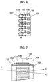
- a first electrode 103 is formed on the entire surface of one side of an acoustic-optical medium 101, and a piezoelectric element 102 is disposed thereon.
- Five second electrodes 104 are provided on the piezoelectric element 102, and thereby five transducers are formed.
- a first lead wire 105 is connected nearly to the center of each second electrode 104, and a second lead wire 106 corresponding to each first lead wire 105 is mutually connected to both ends of the first electrode 103.
- the first lead wire 105 and second lead wire 106 are connected to each driving signal source 107.
- the piezoelectric element 102 is oscillated by an alternating-current signal supplied from the first lead wire 105 and second lead wire 106, and becomes an elastic wave generating source. Therefore, the acoustic-optical medium 101 has as many elastic wave generating sources as the number of transducers, that is, five.
- the generated elastic wave propagates vertically on the transducer mounted surface of the acoustic-optical medium 101, and acts on the light beam passing through the propagation area, thereby generating a diffracted light.
- This mode is shown in Fig. 7.
- "I” denotes an incident light
- "I1" is a diffracted light
- I0" represents a non-diffracted transmission light. Since the diffracted light intensity is proportional to the elastic wave intensity, that is, the driving signal strength, desired optical recording is realized by varying the driving signal strength depending on the recording pattern.
- first lead wires 105 and second lead wires 106 are indicated by coil symbols because they have a very slight inductance.
- Reference numeral 108 indicates an output impedance of the driving signal source 107, and the driving signal sources 107 are commonly grounded by connecting among the transducers.
- the first electrode 103 is commonly shared among the transducers.
- the voltage generated by the inductance of the second lead wire 106 may drive the output impedance 108 and the first electrode 103, or the piezoelectric element 102 of other transducer through the first electrode 103, thereby generating a crosstalk.
- the multi-channel optical modulator of the invention comprises an acoustic-optical medium, a plurality of first electrodes provided on one side of this acoustic-optical medium, a plurality of piezoelectric elements provided on the first electrodes, a plurality of second electrodes provided on the piezoelectric elements, a plurality of first lead wires connected individually to the second electrodes, and a plurality of second lead wires connected individually to the first electrodes, in which the first electrodes are independent of individual transducers, and therefore the voltage generated in the second lead wire of any transducer may not be applied to the piezoelectric element of any other transducer, so that a generation of crosstalk may be prevented.
- first electrodes 13 are formed.
- the acoustic-optical medium 11 is made of tellurium dioxide, lead molybdate, or a similar material allowing to pass light at the wavelength to be modulated, and having a large figure of merit in the acousto-optic effect.
- the acoustic-optical medium 11 has parallel upper and lower surfaces, and the first electrodes 13 are formed on the side vertical to these upper and lower surfaces. The side opposite to the side on which the first electrodes 13 formed is not parallel to the side on which the first electrodes 13 formed.
- a piezoelectric element 12 having a narrower width than the width of the first electrodes 13 is formed.
- the piezoelectric element 12 is made of lithium niobate which is a piezoelectric crystal, and it is compression-bonded onto the first electrodes 13 in a vacuum, and polished to a thickness for resonating at a driving frequency.
- the piezoelectric element 12 is formed so that its width direction end may not coincide with the width direction end of the first electrodes 13, that is, it is deviated in position so that the second lead wires 16 may be formed on the first electrodes 13 in a later process.
- the second electrodes 14 have a three-layer structure, formed of Ni-Cr layer, Cu layer, and Au layer sequentially from the piezoelectric element 12 side.
- the first lead wire 15 is connected electrically by soldering to the second electrode 14 of each transducer. At this time, the first lead wire 15 is alternately connected to the different end from the adjacent second electrode 14. Further, the second lead wire 16 is soldered to the first electrode 13 at the soldering side of the first lead wire 15 of each transducer. At this time, for the ease of soldering of the second lead wires 16, a plating layer 19 of two layers made of lower layer of Cu and upper layer of Au is formed at the soldering position of the second lead wire 16 of the first electrode 13.
- the first lead wire 15 and second lead wire 16 are connected to a driving signal source 17.
- the multi-channel optical modulator having five transducers of the same shape as shown in Fig. 1 and Fig. 2 is formed.
- Fig. 3 is a circuit diagram of this multi-channel optical modulator, in which the first lead wires 15 and second lead wires 16 are indicated by coil symbol because they have, if very slight, an inductance.
- Reference numeral 20 is an output impedance of the driving signal source 17, and the grounding of the driving signal source 17 connected to each transducer is common.
- Each transducer of this multi-channel optical modulator individually has an independent first electrode 13, and the signal of a certain transducer will not be applied to any other transducer through the output impedance 20 or first electrode 13.
Landscapes
- Physics & Mathematics (AREA)
- Nonlinear Science (AREA)
- General Physics & Mathematics (AREA)
- Optics & Photonics (AREA)
- Chemical & Material Sciences (AREA)
- Crystallography & Structural Chemistry (AREA)
- Optical Modulation, Optical Deflection, Nonlinear Optics, Optical Demodulation, Optical Logic Elements (AREA)
Abstract
Description
- 11
- Acoustic-optical medium
- 12
- Piezoelectric element
- 13
- First electrode
- 14
- Second electrode
- 15
- First lead wire
- 16
- Second lead wire
- 17
- Driving signal source
- 18
- Split groove
- 19
- Plating layer
- 20
- Output impedance
- 101
- Acoustic-optical medium
- 102
- Piezoelectric element
- 103
- First electrode
- 104
- Second electrode
- 105
- First lead wire
- 106
- Second lead wire
- 107
- Driving signal source
- 108
- Output impedance
Claims (5)
- A multi-channel optical modulator comprising:an acoustic-optical medium;a plurality of first electrodes provided on one side of the acoustic-optical medium;a plurality of piezoelectric elements provided on the first electrodes;a plurality of second electrodes provided on the piezoelectric elements;a plurality of first lead wires connected individually to the second electrodes; anda plurality of second lead wires connected individually to the first electrodes.
- The multi-channel optical modulator of claim 1, wherein a split groove is provided in the acoustic-optical element between adjacent electrodes of the first electrodes.
- The multi-channel optical modulator of claim 2, wherein the section of the split groove is a curved shape.
- The multi-channel optical modulator of claim 2, wherein the depth of the split groove is deeper than a light beam incident position.
- The multi-channel optical modulator of claim 1, whereinthe first lead wires are connected to one end of the second electrodes,the adjoining first lead wires are connected to other end of the second electrodes, andthe second lead wires making pairs with the first lead wires are connected to the first electrodes close to the first lead wires.
Applications Claiming Priority (3)
| Application Number | Priority Date | Filing Date | Title |
|---|---|---|---|
| JP11027586A JP2000221460A (en) | 1999-02-04 | 1999-02-04 | Multi-channel light modulator |
| JP2758699 | 1999-02-04 | ||
| PCT/JP2000/000549 WO2000046630A1 (en) | 1999-02-04 | 2000-02-02 | Multichannel optical modulation element |
Publications (2)
| Publication Number | Publication Date |
|---|---|
| EP1076256A1 true EP1076256A1 (en) | 2001-02-14 |
| EP1076256A4 EP1076256A4 (en) | 2003-05-28 |
Family
ID=12225068
Family Applications (1)
| Application Number | Title | Priority Date | Filing Date |
|---|---|---|---|
| EP00902044A Withdrawn EP1076256A4 (en) | 1999-02-04 | 2000-02-02 | MULTI-CHANNEL OPTICAL MODULATION ELEMENT |
Country Status (4)
| Country | Link |
|---|---|
| US (1) | US6449083B1 (en) |
| EP (1) | EP1076256A4 (en) |
| JP (1) | JP2000221460A (en) |
| WO (1) | WO2000046630A1 (en) |
Cited By (1)
| Publication number | Priority date | Publication date | Assignee | Title |
|---|---|---|---|---|
| EP1500966A3 (en) * | 2003-06-23 | 2005-03-16 | Matsushita Electric Industrial Co., Ltd. | Acousto optic element |
Families Citing this family (10)
| Publication number | Priority date | Publication date | Assignee | Title |
|---|---|---|---|---|
| US6549247B2 (en) * | 2001-03-06 | 2003-04-15 | Kohji Toda | Ultrasonic liquid-crystal display |
| KR100459899B1 (en) * | 2002-03-12 | 2004-12-04 | 삼성전자주식회사 | Laser video projector having multi-channel acoustic optic modulator, method and circuit of driving the same |
| EP1811378A2 (en) * | 2006-01-23 | 2007-07-25 | Xyratex Technology Limited | A computer system, a computer and a method of storing a data file |
| US7538929B2 (en) | 2007-04-06 | 2009-05-26 | Harris Corporation | RF phase modulation technique for performing acousto-optic intensity modulation of an optical wavefront |
| US7667888B2 (en) * | 2007-04-06 | 2010-02-23 | Harris Corporation | Low cost system and method that implements acousto-optic (AO) RF signal excitation |
| US7518779B2 (en) * | 2007-04-06 | 2009-04-14 | Harris Corporation | Acousto-optic devices having extended temperature reliability |
| US11327348B2 (en) * | 2018-09-18 | 2022-05-10 | Eagle Technology, Llc | Multi-channel laser system including optical assembly with etched optical signal channels and related methods |
| US11042052B2 (en) * | 2018-09-18 | 2021-06-22 | Eagle Technology, Llc | Multi-channel laser system including an acousto-optic modulator (AOM) with beam polarization switching and related methods |
| US11813697B1 (en) * | 2023-04-07 | 2023-11-14 | Intraaction Corp | Laser methods of fabrication of clothing |
| US11906874B1 (en) * | 2023-04-07 | 2024-02-20 | Intraaction Corp | Acousto-optic deflector and methods of fabrication |
Family Cites Families (16)
| Publication number | Priority date | Publication date | Assignee | Title |
|---|---|---|---|---|
| US4000493A (en) * | 1971-04-12 | 1976-12-28 | Eastman Kodak Company | Acoustooptic scanner apparatus and method |
| JPS5732424A (en) * | 1980-08-06 | 1982-02-22 | Teikoku Tsushin Kogyo Kk | Acoustooptic diffraction element |
| JPS5764216A (en) * | 1980-10-06 | 1982-04-19 | Ricoh Co Ltd | Manufacture of acoustooptic element |
| DE3382323D1 (en) * | 1982-07-27 | 1991-08-01 | Hoya Corp | ACOUSTOOPTIC MODULATION ELEMENT AND DEVICE WITH SUCH AN ELEMENT. |
| JPS5919922A (en) * | 1982-07-27 | 1984-02-01 | Hoya Corp | Acoustooptic modulating element |
| US4555160A (en) * | 1982-08-02 | 1985-11-26 | Westinghouse Electric Corp. | Method and apparatus for strain relieving transducers bonded to acousto-optic devices |
| JPS61109022A (en) * | 1984-11-01 | 1986-05-27 | Nec Corp | Ultrasonic wave optical modulator |
| JPS63118712A (en) * | 1986-11-07 | 1988-05-23 | Matsushita Electric Ind Co Ltd | acousto-optic element |
| JPH01131526A (en) * | 1987-11-17 | 1989-05-24 | Matsushita Electric Ind Co Ltd | Multi-channel optical modulator |
| JPH04155310A (en) * | 1990-10-18 | 1992-05-28 | Matsushita Electric Ind Co Ltd | acousto-optic element |
| JPH0818328B2 (en) * | 1991-07-26 | 1996-02-28 | 憲一 石川 | Cutting method of hard brittle material with peripheral blade |
| JP3283047B2 (en) * | 1991-10-07 | 2002-05-20 | 株式会社東芝 | Semiconductor device and method of manufacturing semiconductor device |
| JPH06226972A (en) * | 1993-02-01 | 1994-08-16 | Brother Ind Ltd | Ink jet apparatus |
| JP2976273B2 (en) * | 1995-03-24 | 1999-11-10 | 株式会社村田製作所 | Acousto-optic element |
| KR100188987B1 (en) * | 1996-09-06 | 1999-06-01 | 박원훈 | Multi-channel acoustic-optic modulator, the aperture of each modulating cell connected in one row |
| KR100292407B1 (en) * | 1998-10-07 | 2001-06-01 | 윤종용 | Semiconductor deivce comprising deposited materials for relieving the stress and method for fabricating the same |
-
1999
- 1999-02-04 JP JP11027586A patent/JP2000221460A/en active Pending
-
2000
- 2000-02-02 US US09/647,597 patent/US6449083B1/en not_active Expired - Fee Related
- 2000-02-02 EP EP00902044A patent/EP1076256A4/en not_active Withdrawn
- 2000-02-02 WO PCT/JP2000/000549 patent/WO2000046630A1/en not_active Ceased
Cited By (2)
| Publication number | Priority date | Publication date | Assignee | Title |
|---|---|---|---|---|
| EP1500966A3 (en) * | 2003-06-23 | 2005-03-16 | Matsushita Electric Industrial Co., Ltd. | Acousto optic element |
| US7054055B2 (en) | 2003-06-23 | 2006-05-30 | Matsushita Electric Industrial Co., Ltd. | Acousto optic element |
Also Published As
| Publication number | Publication date |
|---|---|
| JP2000221460A (en) | 2000-08-11 |
| WO2000046630A1 (en) | 2000-08-10 |
| EP1076256A4 (en) | 2003-05-28 |
| US6449083B1 (en) | 2002-09-10 |
Similar Documents
| Publication | Publication Date | Title |
|---|---|---|
| US6449083B1 (en) | Multi-channel optical modulator | |
| EP0145429B1 (en) | Curvilinear array of ultrasonic transducers | |
| CN107567682B (en) | Plate wave device with wave confinement structure and method of manufacture | |
| EP0379229B1 (en) | Ultrasonic probe | |
| US3924931A (en) | Integrated optical signal processing system | |
| KR19980020201A (en) | Multi-channel acoustic light modulator with openings in each cell lined up | |
| US12461402B2 (en) | Acousto-optic modulator system and device with connections and related methods | |
| EP0100238B1 (en) | Acoustooptic modulation element and system | |
| US4381887A (en) | Simplified acousto-optic deflector using electronic delays | |
| US4671620A (en) | Phased-array acousto-optic Bragg cell | |
| WO2001014925A1 (en) | Thermally balanced acousto-optic modulator | |
| CA1082798A (en) | Magnetostrictive elastic surface wave structure | |
| US4477892A (en) | Surface acoustic wave device having a pyramid shaped tip for recording video information on a substrate | |
| CA2296278A1 (en) | Acousto-optic modulator array with reduced rf crosstalk | |
| US4434481A (en) | Traveling wave surface acoustic wave transducer | |
| US20020141030A1 (en) | Opposing electrode light modulator array and method for manufacturing the same | |
| EP1526402A2 (en) | Optical device module | |
| US5048936A (en) | Light beam deflector | |
| JP2827125B2 (en) | Acousto-optic element | |
| JPS6016484A (en) | Semiconductor laser | |
| JPH01107212A (en) | Optical waveguide element | |
| SU989520A1 (en) | Multi-channel acoustooptic deflector | |
| JPH06110025A (en) | Optical external modulator | |
| JPH06123864A (en) | Optical shutter array element and manufacturing method thereof | |
| JPH01131525A (en) | Multi-channel optical modulator |
Legal Events
| Date | Code | Title | Description |
|---|---|---|---|
| PUAI | Public reference made under article 153(3) epc to a published international application that has entered the european phase |
Free format text: ORIGINAL CODE: 0009012 |
|
| 17P | Request for examination filed |
Effective date: 20001024 |
|
| AK | Designated contracting states |
Kind code of ref document: A1 Designated state(s): AT BE CH CY DE DK ES FI FR GB GR IE IT LI LU MC NL PT SE |
|
| A4 | Supplementary search report drawn up and despatched |
Effective date: 20030414 |
|
| RIC1 | Information provided on ipc code assigned before grant |
Ipc: 7G 02F 1/33 B Ipc: 7G 02F 1/11 A |
|
| 17Q | First examination report despatched |
Effective date: 20030825 |
|
| RBV | Designated contracting states (corrected) |
Designated state(s): DE FR GB |
|
| RAP1 | Party data changed (applicant data changed or rights of an application transferred) |
Owner name: PANASONIC CORPORATION |
|
| STAA | Information on the status of an ep patent application or granted ep patent |
Free format text: STATUS: THE APPLICATION IS DEEMED TO BE WITHDRAWN |
|
| 18D | Application deemed to be withdrawn |
Effective date: 20100901 |