EP1075670B1 - Shutter mode microencapsulated electrophoretic display - Google Patents
Shutter mode microencapsulated electrophoretic display Download PDFInfo
- Publication number
- EP1075670B1 EP1075670B1 EP99920099A EP99920099A EP1075670B1 EP 1075670 B1 EP1075670 B1 EP 1075670B1 EP 99920099 A EP99920099 A EP 99920099A EP 99920099 A EP99920099 A EP 99920099A EP 1075670 B1 EP1075670 B1 EP 1075670B1
- Authority
- EP
- European Patent Office
- Prior art keywords
- particles
- electrode
- electrophoretic display
- capsule
- display
- Prior art date
- Legal status (The legal status is an assumption and is not a legal conclusion. Google has not performed a legal analysis and makes no representation as to the accuracy of the status listed.)
- Expired - Lifetime
Links
- 239000002245 particle Substances 0.000 claims description 105
- 239000002775 capsule Substances 0.000 claims description 82
- 239000012530 fluid Substances 0.000 claims description 46
- 239000000758 substrate Substances 0.000 claims description 28
- 230000003287 optical effect Effects 0.000 claims description 25
- 230000005684 electric field Effects 0.000 claims description 21
- 230000000717 retained effect Effects 0.000 claims description 6
- 239000000976 ink Substances 0.000 description 30
- 239000000463 material Substances 0.000 description 17
- 238000000034 method Methods 0.000 description 17
- 238000000576 coating method Methods 0.000 description 11
- 229920000642 polymer Polymers 0.000 description 11
- -1 polyphenylenevinylene Polymers 0.000 description 11
- 230000008569 process Effects 0.000 description 11
- 239000004020 conductor Substances 0.000 description 10
- 239000011248 coating agent Substances 0.000 description 9
- 239000003094 microcapsule Substances 0.000 description 9
- 238000007639 printing Methods 0.000 description 8
- 230000000007 visual effect Effects 0.000 description 8
- 230000000694 effects Effects 0.000 description 7
- 239000000203 mixture Substances 0.000 description 6
- 239000011230 binding agent Substances 0.000 description 5
- 239000003086 colorant Substances 0.000 description 5
- AMGQUBHHOARCQH-UHFFFAOYSA-N indium;oxotin Chemical compound [In].[Sn]=O AMGQUBHHOARCQH-UHFFFAOYSA-N 0.000 description 5
- 239000000049 pigment Substances 0.000 description 5
- 239000004973 liquid crystal related substance Substances 0.000 description 4
- 239000003960 organic solvent Substances 0.000 description 4
- SNRUBQQJIBEYMU-UHFFFAOYSA-N Dodecane Natural products CCCCCCCCCCCC SNRUBQQJIBEYMU-UHFFFAOYSA-N 0.000 description 3
- YXFVVABEGXRONW-UHFFFAOYSA-N Toluene Chemical compound CC1=CC=CC=C1 YXFVVABEGXRONW-UHFFFAOYSA-N 0.000 description 3
- 230000008901 benefit Effects 0.000 description 3
- 238000004049 embossing Methods 0.000 description 3
- 238000004519 manufacturing process Methods 0.000 description 3
- 229920000767 polyaniline Polymers 0.000 description 3
- OKTJSMMVPCPJKN-UHFFFAOYSA-N Carbon Chemical compound [C] OKTJSMMVPCPJKN-UHFFFAOYSA-N 0.000 description 2
- UFWIBTONFRDIAS-UHFFFAOYSA-N Naphthalene Chemical compound C1=CC=CC2=CC=CC=C21 UFWIBTONFRDIAS-UHFFFAOYSA-N 0.000 description 2
- BQCADISMDOOEFD-UHFFFAOYSA-N Silver Chemical compound [Ag] BQCADISMDOOEFD-UHFFFAOYSA-N 0.000 description 2
- 239000011149 active material Substances 0.000 description 2
- 230000005540 biological transmission Effects 0.000 description 2
- 229920001940 conductive polymer Polymers 0.000 description 2
- 239000012769 display material Substances 0.000 description 2
- 238000005530 etching Methods 0.000 description 2
- 239000011521 glass Substances 0.000 description 2
- 229910002804 graphite Inorganic materials 0.000 description 2
- 239000010439 graphite Substances 0.000 description 2
- 229910052736 halogen Inorganic materials 0.000 description 2
- 150000002367 halogens Chemical class 0.000 description 2
- 229930195733 hydrocarbon Natural products 0.000 description 2
- 150000002430 hydrocarbons Chemical class 0.000 description 2
- 230000003993 interaction Effects 0.000 description 2
- 238000009685 knife-over-roll coating Methods 0.000 description 2
- 230000005499 meniscus Effects 0.000 description 2
- 229910052751 metal Inorganic materials 0.000 description 2
- 239000002184 metal Substances 0.000 description 2
- 230000005012 migration Effects 0.000 description 2
- 238000013508 migration Methods 0.000 description 2
- 229920002493 poly(chlorotrifluoroethylene) Polymers 0.000 description 2
- 229920000553 poly(phenylenevinylene) Polymers 0.000 description 2
- 229920000123 polythiophene Polymers 0.000 description 2
- 239000000843 powder Substances 0.000 description 2
- 238000007763 reverse roll coating Methods 0.000 description 2
- 229920002545 silicone oil Polymers 0.000 description 2
- 229910052709 silver Inorganic materials 0.000 description 2
- 239000004332 silver Substances 0.000 description 2
- 239000002904 solvent Substances 0.000 description 2
- 238000004528 spin coating Methods 0.000 description 2
- 238000005507 spraying Methods 0.000 description 2
- 239000000126 substance Substances 0.000 description 2
- VZGDMQKNWNREIO-UHFFFAOYSA-N tetrachloromethane Chemical compound ClC(Cl)(Cl)Cl VZGDMQKNWNREIO-UHFFFAOYSA-N 0.000 description 2
- BGHCVCJVXZWKCC-UHFFFAOYSA-N tetradecane Chemical compound CCCCCCCCCCCCCC BGHCVCJVXZWKCC-UHFFFAOYSA-N 0.000 description 2
- SKYXLDSRLNRAPS-UHFFFAOYSA-N 1,2,4-trifluoro-5-methoxybenzene Chemical compound COC1=CC(F)=C(F)C=C1F SKYXLDSRLNRAPS-UHFFFAOYSA-N 0.000 description 1
- RYGMFSIKBFXOCR-UHFFFAOYSA-N Copper Chemical compound [Cu] RYGMFSIKBFXOCR-UHFFFAOYSA-N 0.000 description 1
- 239000004642 Polyimide Substances 0.000 description 1
- SZKKRCSOSQAJDE-UHFFFAOYSA-N Schradan Chemical group CN(C)P(=O)(N(C)C)OP(=O)(N(C)C)N(C)C SZKKRCSOSQAJDE-UHFFFAOYSA-N 0.000 description 1
- QYKIQEUNHZKYBP-UHFFFAOYSA-N Vinyl ether Chemical class C=COC=C QYKIQEUNHZKYBP-UHFFFAOYSA-N 0.000 description 1
- 238000007754 air knife coating Methods 0.000 description 1
- 150000001338 aliphatic hydrocarbons Chemical class 0.000 description 1
- 150000004945 aromatic hydrocarbons Chemical class 0.000 description 1
- 230000000903 blocking effect Effects 0.000 description 1
- 238000009835 boiling Methods 0.000 description 1
- QXJJQWWVWRCVQT-UHFFFAOYSA-K calcium;sodium;phosphate Chemical compound [Na+].[Ca+2].[O-]P([O-])([O-])=O QXJJQWWVWRCVQT-UHFFFAOYSA-K 0.000 description 1
- 238000007385 chemical modification Methods 0.000 description 1
- 239000003795 chemical substances by application Substances 0.000 description 1
- 239000000084 colloidal system Substances 0.000 description 1
- 230000000295 complement effect Effects 0.000 description 1
- 239000002131 composite material Substances 0.000 description 1
- 238000010276 construction Methods 0.000 description 1
- 239000002872 contrast media Substances 0.000 description 1
- 229940039231 contrast media Drugs 0.000 description 1
- 229910052802 copper Inorganic materials 0.000 description 1
- 239000010949 copper Substances 0.000 description 1
- 238000007766 curtain coating Methods 0.000 description 1
- 238000000151 deposition Methods 0.000 description 1
- 230000008021 deposition Effects 0.000 description 1
- 238000007607 die coating method Methods 0.000 description 1
- 239000004205 dimethyl polysiloxane Substances 0.000 description 1
- 238000003618 dip coating Methods 0.000 description 1
- 238000009826 distribution Methods 0.000 description 1
- 230000005611 electricity Effects 0.000 description 1
- 238000005538 encapsulation Methods 0.000 description 1
- 150000002118 epoxides Chemical class 0.000 description 1
- 150000002170 ethers Chemical class 0.000 description 1
- 238000007765 extrusion coating Methods 0.000 description 1
- 239000000796 flavoring agent Substances 0.000 description 1
- 235000019634 flavors Nutrition 0.000 description 1
- 239000003205 fragrance Substances 0.000 description 1
- 230000005484 gravity Effects 0.000 description 1
- 238000007756 gravure coating Methods 0.000 description 1
- 150000008282 halocarbons Chemical class 0.000 description 1
- UQEAIHBTYFGYIE-UHFFFAOYSA-N hexamethyldisiloxane Chemical compound C[Si](C)(C)O[Si](C)(C)C UQEAIHBTYFGYIE-UHFFFAOYSA-N 0.000 description 1
- 238000007641 inkjet printing Methods 0.000 description 1
- 239000007788 liquid Substances 0.000 description 1
- 239000011159 matrix material Substances 0.000 description 1
- 239000012528 membrane Substances 0.000 description 1
- 238000005459 micromachining Methods 0.000 description 1
- 239000003607 modifier Substances 0.000 description 1
- 239000000178 monomer Substances 0.000 description 1
- DIOQZVSQGTUSAI-UHFFFAOYSA-N n-butylhexane Natural products CCCCCCCCCC DIOQZVSQGTUSAI-UHFFFAOYSA-N 0.000 description 1
- 150000002790 naphthalenes Chemical class 0.000 description 1
- 239000003921 oil Substances 0.000 description 1
- SLIUAWYAILUBJU-UHFFFAOYSA-N pentacene Chemical compound C1=CC=CC2=CC3=CC4=CC5=CC=CC=C5C=C4C=C3C=C21 SLIUAWYAILUBJU-UHFFFAOYSA-N 0.000 description 1
- 230000002085 persistent effect Effects 0.000 description 1
- 239000003208 petroleum Substances 0.000 description 1
- IEQIEDJGQAUEQZ-UHFFFAOYSA-N phthalocyanine Chemical compound N1C(N=C2C3=CC=CC=C3C(N=C3C4=CC=CC=C4C(=N4)N3)=N2)=C(C=CC=C2)C2=C1N=C1C2=CC=CC=C2C4=N1 IEQIEDJGQAUEQZ-UHFFFAOYSA-N 0.000 description 1
- 230000000704 physical effect Effects 0.000 description 1
- 239000004033 plastic Substances 0.000 description 1
- 229920003023 plastic Polymers 0.000 description 1
- 229920000435 poly(dimethylsiloxane) Polymers 0.000 description 1
- 229920003216 poly(methylphenylsiloxane) Polymers 0.000 description 1
- 229920001721 polyimide Polymers 0.000 description 1
- 238000006116 polymerization reaction Methods 0.000 description 1
- 229920000128 polypyrrole Polymers 0.000 description 1
- 239000000376 reactant Substances 0.000 description 1
- 229920006395 saturated elastomer Polymers 0.000 description 1
- 238000007650 screen-printing Methods 0.000 description 1
- 229910000679 solder Inorganic materials 0.000 description 1
- 239000007787 solid Substances 0.000 description 1
- 239000010421 standard material Substances 0.000 description 1
- 238000007651 thermal printing Methods 0.000 description 1
- XOLBLPGZBRYERU-UHFFFAOYSA-N tin dioxide Chemical compound O=[Sn]=O XOLBLPGZBRYERU-UHFFFAOYSA-N 0.000 description 1
- 229910001887 tin oxide Inorganic materials 0.000 description 1
- 230000007704 transition Effects 0.000 description 1
- 239000012780 transparent material Substances 0.000 description 1
Images

Classifications
-
- G—PHYSICS
- G09—EDUCATION; CRYPTOGRAPHY; DISPLAY; ADVERTISING; SEALS
- G09F—DISPLAYING; ADVERTISING; SIGNS; LABELS OR NAME-PLATES; SEALS
- G09F9/00—Indicating arrangements for variable information in which the information is built-up on a support by selection or combination of individual elements
- G09F9/30—Indicating arrangements for variable information in which the information is built-up on a support by selection or combination of individual elements in which the desired character or characters are formed by combining individual elements
- G09F9/37—Indicating arrangements for variable information in which the information is built-up on a support by selection or combination of individual elements in which the desired character or characters are formed by combining individual elements being movable elements
- G09F9/372—Indicating arrangements for variable information in which the information is built-up on a support by selection or combination of individual elements in which the desired character or characters are formed by combining individual elements being movable elements the positions of the elements being controlled by the application of an electric field
-
- B—PERFORMING OPERATIONS; TRANSPORTING
- B41—PRINTING; LINING MACHINES; TYPEWRITERS; STAMPS
- B41J—TYPEWRITERS; SELECTIVE PRINTING MECHANISMS, i.e. MECHANISMS PRINTING OTHERWISE THAN FROM A FORME; CORRECTION OF TYPOGRAPHICAL ERRORS
- B41J3/00—Typewriters or selective printing or marking mechanisms characterised by the purpose for which they are constructed
- B41J3/407—Typewriters or selective printing or marking mechanisms characterised by the purpose for which they are constructed for marking on special material
- B41J3/4076—Typewriters or selective printing or marking mechanisms characterised by the purpose for which they are constructed for marking on special material printing on rewritable, bistable "electronic paper" by a focused electric or magnetic field
-
- G—PHYSICS
- G02—OPTICS
- G02B—OPTICAL ELEMENTS, SYSTEMS OR APPARATUS
- G02B26/00—Optical devices or arrangements for the control of light using movable or deformable optical elements
- G02B26/02—Optical devices or arrangements for the control of light using movable or deformable optical elements for controlling the intensity of light
- G02B26/026—Optical devices or arrangements for the control of light using movable or deformable optical elements for controlling the intensity of light based on the rotation of particles under the influence of an external field, e.g. gyricons, twisting ball displays
-
- G—PHYSICS
- G02—OPTICS
- G02F—OPTICAL DEVICES OR ARRANGEMENTS FOR THE CONTROL OF LIGHT BY MODIFICATION OF THE OPTICAL PROPERTIES OF THE MEDIA OF THE ELEMENTS INVOLVED THEREIN; NON-LINEAR OPTICS; FREQUENCY-CHANGING OF LIGHT; OPTICAL LOGIC ELEMENTS; OPTICAL ANALOGUE/DIGITAL CONVERTERS
- G02F1/00—Devices or arrangements for the control of the intensity, colour, phase, polarisation or direction of light arriving from an independent light source, e.g. switching, gating or modulating; Non-linear optics
- G02F1/01—Devices or arrangements for the control of the intensity, colour, phase, polarisation or direction of light arriving from an independent light source, e.g. switching, gating or modulating; Non-linear optics for the control of the intensity, phase, polarisation or colour
- G02F1/13—Devices or arrangements for the control of the intensity, colour, phase, polarisation or direction of light arriving from an independent light source, e.g. switching, gating or modulating; Non-linear optics for the control of the intensity, phase, polarisation or colour based on liquid crystals, e.g. single liquid crystal display cells
- G02F1/133—Constructional arrangements; Operation of liquid crystal cells; Circuit arrangements
- G02F1/1333—Constructional arrangements; Manufacturing methods
- G02F1/1345—Conductors connecting electrodes to cell terminals
-
- G—PHYSICS
- G02—OPTICS
- G02F—OPTICAL DEVICES OR ARRANGEMENTS FOR THE CONTROL OF LIGHT BY MODIFICATION OF THE OPTICAL PROPERTIES OF THE MEDIA OF THE ELEMENTS INVOLVED THEREIN; NON-LINEAR OPTICS; FREQUENCY-CHANGING OF LIGHT; OPTICAL LOGIC ELEMENTS; OPTICAL ANALOGUE/DIGITAL CONVERTERS
- G02F1/00—Devices or arrangements for the control of the intensity, colour, phase, polarisation or direction of light arriving from an independent light source, e.g. switching, gating or modulating; Non-linear optics
- G02F1/01—Devices or arrangements for the control of the intensity, colour, phase, polarisation or direction of light arriving from an independent light source, e.g. switching, gating or modulating; Non-linear optics for the control of the intensity, phase, polarisation or colour
- G02F1/165—Devices or arrangements for the control of the intensity, colour, phase, polarisation or direction of light arriving from an independent light source, e.g. switching, gating or modulating; Non-linear optics for the control of the intensity, phase, polarisation or colour based on translational movement of particles in a fluid under the influence of an applied field
- G02F1/166—Devices or arrangements for the control of the intensity, colour, phase, polarisation or direction of light arriving from an independent light source, e.g. switching, gating or modulating; Non-linear optics for the control of the intensity, phase, polarisation or colour based on translational movement of particles in a fluid under the influence of an applied field characterised by the electro-optical or magneto-optical effect
- G02F1/167—Devices or arrangements for the control of the intensity, colour, phase, polarisation or direction of light arriving from an independent light source, e.g. switching, gating or modulating; Non-linear optics for the control of the intensity, phase, polarisation or colour based on translational movement of particles in a fluid under the influence of an applied field characterised by the electro-optical or magneto-optical effect by electrophoresis
-
- G—PHYSICS
- G02—OPTICS
- G02F—OPTICAL DEVICES OR ARRANGEMENTS FOR THE CONTROL OF LIGHT BY MODIFICATION OF THE OPTICAL PROPERTIES OF THE MEDIA OF THE ELEMENTS INVOLVED THEREIN; NON-LINEAR OPTICS; FREQUENCY-CHANGING OF LIGHT; OPTICAL LOGIC ELEMENTS; OPTICAL ANALOGUE/DIGITAL CONVERTERS
- G02F1/00—Devices or arrangements for the control of the intensity, colour, phase, polarisation or direction of light arriving from an independent light source, e.g. switching, gating or modulating; Non-linear optics
- G02F1/01—Devices or arrangements for the control of the intensity, colour, phase, polarisation or direction of light arriving from an independent light source, e.g. switching, gating or modulating; Non-linear optics for the control of the intensity, phase, polarisation or colour
- G02F1/165—Devices or arrangements for the control of the intensity, colour, phase, polarisation or direction of light arriving from an independent light source, e.g. switching, gating or modulating; Non-linear optics for the control of the intensity, phase, polarisation or colour based on translational movement of particles in a fluid under the influence of an applied field
- G02F1/1675—Constructional details
- G02F1/16757—Microcapsules
-
- G—PHYSICS
- G09—EDUCATION; CRYPTOGRAPHY; DISPLAY; ADVERTISING; SEALS
- G09F—DISPLAYING; ADVERTISING; SIGNS; LABELS OR NAME-PLATES; SEALS
- G09F9/00—Indicating arrangements for variable information in which the information is built-up on a support by selection or combination of individual elements
- G09F9/30—Indicating arrangements for variable information in which the information is built-up on a support by selection or combination of individual elements in which the desired character or characters are formed by combining individual elements
- G09F9/302—Indicating arrangements for variable information in which the information is built-up on a support by selection or combination of individual elements in which the desired character or characters are formed by combining individual elements characterised by the form or geometrical disposition of the individual elements
-
- G—PHYSICS
- G02—OPTICS
- G02F—OPTICAL DEVICES OR ARRANGEMENTS FOR THE CONTROL OF LIGHT BY MODIFICATION OF THE OPTICAL PROPERTIES OF THE MEDIA OF THE ELEMENTS INVOLVED THEREIN; NON-LINEAR OPTICS; FREQUENCY-CHANGING OF LIGHT; OPTICAL LOGIC ELEMENTS; OPTICAL ANALOGUE/DIGITAL CONVERTERS
- G02F1/00—Devices or arrangements for the control of the intensity, colour, phase, polarisation or direction of light arriving from an independent light source, e.g. switching, gating or modulating; Non-linear optics
- G02F1/01—Devices or arrangements for the control of the intensity, colour, phase, polarisation or direction of light arriving from an independent light source, e.g. switching, gating or modulating; Non-linear optics for the control of the intensity, phase, polarisation or colour
- G02F1/13—Devices or arrangements for the control of the intensity, colour, phase, polarisation or direction of light arriving from an independent light source, e.g. switching, gating or modulating; Non-linear optics for the control of the intensity, phase, polarisation or colour based on liquid crystals, e.g. single liquid crystal display cells
- G02F1/133—Constructional arrangements; Operation of liquid crystal cells; Circuit arrangements
- G02F1/1333—Constructional arrangements; Manufacturing methods
- G02F1/133305—Flexible substrates, e.g. plastics, organic film
-
- G—PHYSICS
- G02—OPTICS
- G02F—OPTICAL DEVICES OR ARRANGEMENTS FOR THE CONTROL OF LIGHT BY MODIFICATION OF THE OPTICAL PROPERTIES OF THE MEDIA OF THE ELEMENTS INVOLVED THEREIN; NON-LINEAR OPTICS; FREQUENCY-CHANGING OF LIGHT; OPTICAL LOGIC ELEMENTS; OPTICAL ANALOGUE/DIGITAL CONVERTERS
- G02F1/00—Devices or arrangements for the control of the intensity, colour, phase, polarisation or direction of light arriving from an independent light source, e.g. switching, gating or modulating; Non-linear optics
- G02F1/01—Devices or arrangements for the control of the intensity, colour, phase, polarisation or direction of light arriving from an independent light source, e.g. switching, gating or modulating; Non-linear optics for the control of the intensity, phase, polarisation or colour
- G02F1/13—Devices or arrangements for the control of the intensity, colour, phase, polarisation or direction of light arriving from an independent light source, e.g. switching, gating or modulating; Non-linear optics for the control of the intensity, phase, polarisation or colour based on liquid crystals, e.g. single liquid crystal display cells
- G02F1/133—Constructional arrangements; Operation of liquid crystal cells; Circuit arrangements
- G02F1/1333—Constructional arrangements; Manufacturing methods
- G02F1/1334—Constructional arrangements; Manufacturing methods based on polymer dispersed liquid crystals, e.g. microencapsulated liquid crystals
-
- G—PHYSICS
- G02—OPTICS
- G02F—OPTICAL DEVICES OR ARRANGEMENTS FOR THE CONTROL OF LIGHT BY MODIFICATION OF THE OPTICAL PROPERTIES OF THE MEDIA OF THE ELEMENTS INVOLVED THEREIN; NON-LINEAR OPTICS; FREQUENCY-CHANGING OF LIGHT; OPTICAL LOGIC ELEMENTS; OPTICAL ANALOGUE/DIGITAL CONVERTERS
- G02F2202/00—Materials and properties
- G02F2202/28—Adhesive materials or arrangements
-
- H—ELECTRICITY
- H10—SEMICONDUCTOR DEVICES; ELECTRIC SOLID-STATE DEVICES NOT OTHERWISE PROVIDED FOR
- H10K—ORGANIC ELECTRIC SOLID-STATE DEVICES
- H10K10/00—Organic devices specially adapted for rectifying, amplifying, oscillating or switching; Organic capacitors or resistors having potential barriers
- H10K10/40—Organic transistors
- H10K10/46—Field-effect transistors, e.g. organic thin-film transistors [OTFT]
- H10K10/462—Insulated gate field-effect transistors [IGFETs]
-
- H—ELECTRICITY
- H10—SEMICONDUCTOR DEVICES; ELECTRIC SOLID-STATE DEVICES NOT OTHERWISE PROVIDED FOR
- H10K—ORGANIC ELECTRIC SOLID-STATE DEVICES
- H10K85/00—Organic materials used in the body or electrodes of devices covered by this subclass
- H10K85/30—Coordination compounds
-
- H—ELECTRICITY
- H10—SEMICONDUCTOR DEVICES; ELECTRIC SOLID-STATE DEVICES NOT OTHERWISE PROVIDED FOR
- H10K—ORGANIC ELECTRIC SOLID-STATE DEVICES
- H10K85/00—Organic materials used in the body or electrodes of devices covered by this subclass
- H10K85/60—Organic compounds having low molecular weight
Definitions
- the present invention relates to encapsulated electrophoretic displays and, in particular, to shutter mode encapsulated electrophoretic displays.
- a first electrode structure controls all the segments of the display that may be addressed, that is, changed from one visual state to another.
- a second electrode sometimes called a counter electrode, addresses all display segments as one large electrode, and is generally designed not to overlap any of the rear electrode wire connections that are not desired in the final image.
- the second electrode is also patterned to control specific segments of the display. In these displays, unaddressed areas of the display have a defined appearance.
- Electrophoretic display media generally characterized by the movement of particles through an applied electric field, are highly reflective, can be made bistable, and consume very little power. Encapsulated electrophoretic displays also enable the display to be printed. These properties allow encapsulated electrophoretic display media to be used in many applications for which traditional electronic displays are not suitable, such as flexible displays. The electro-optical properties of encapsulated displays allow, and in some cases require, novel schemes or configurations to be used to address the displays.
- “Shutter mode” electrophoretic displays are configured so that the particles can switch between a largely light-blocking (or reflecting) state and a largely light-transmitting state. These displays often are constructed with particles which can migrate between a smaller and larger electrode. Migration of the particles to the large electrodes allows them to spread out, causing the capsule to take on the visual properties of the particles. Migration of the particles to the smaller electrode causes the capsule to take on the visual properties of the dispersing fluid or of the larger electrode, because the particles are "clumped" together near the smaller electrode. Another use of this effect is to control transmission of light through the capsule.
- the drawback to shutter mode displays is that the electrodes must be etched very precisely.
- This invention seeks to provide a highly-flexible, reflective display which can be manufactured easily, consumes little (or none in the case of bistable displays) power, and can, therefore, be incorporated into a variety of applications.
- the invention may be in form of a printable display comprising an encapsulated electrophoretic display medium.
- the resulting display may be flexible. Since the display media can be printed, the display itself can be made inexpensively.
- the present invention allows shutter mode electrophoretic displays to be fabricated without requiring finely etched electrodes.
- An encapsulated electrophoretic display can be constructed so that the optical state of the display is stable for some length of time.
- the display When the display has two states which are stable in this manner, the display is said to be bistable. If more than two states of the display are stable, then the display can be said to be multistable.
- bistable will be used to indicate a display in which any optical state remains fixed once the addressing voltage is removed.
- the definition of a bistable state depends on the application for the display.
- a slowly-decaying optical state can be effectively bistable if the optical state is substantially unchanged over the required viewing time. For example, in a display which is updated every few minutes, a display image which is stable for hours or days is effectively bistable for that application.
- bistable also indicates a display with an optical state sufficiently long-lived as to be effectively bistable for the application in mind.
- encapsulated electrophoretic displays in which the image decays quickly once the addressing voltage to the display is removed (i.e., the display is not bistable or multistable).
- an encapsulated electrophoretic display which is not bistable. Whether or not an encapsulated electrophoretic display is bistable, and its degree of bistability, can be controlled through appropriate chemical modification of the electrophoretic particles, the suspending fluid, the capsule, and binder materials.
- An encapsulated electrophoretic display may take many forms.
- the display comprises capsules.
- the capsules may be of any size or shape.
- the capsules are formed by an encapsulation technique, as described below.
- Particles are encapsulated in the capsules.
- the particles may be one or more different types of particles.
- the particles may be colored, luminescent, light-absorbing or transparent, for example.
- the particles may include neat pigments, dyed (laked) pigments or pigment/polymer composites, for example.
- the capsules further comprise a suspending fluid in which the particles are dispersed.
- an encapsulated electrophoretic display requires the proper interaction of several different types of materials and processes, such as a polymeric binder and, optionally, a capsule membrane. These materials must be chemically compatible with the electrophoretic particles and fluid, as well as with each other. The capsule materials may engage in useful surface interactions with the electrophoretic particles, or may act as a chemical or physical boundary between the fluid and the binder.
- printing is intended to include all forms of printing and coating, including: premetered coatings such as patch die coating, slot or extrusion coating, slide or cascade coating, and curtain coating; roll coating such as knife over roll coating, forward and reverse roll coating; gravure coating; dip coating; spray coating; meniscus coating; spin coating; brush coating; air knife coating; silk screen printing processes; electrostatic printing processes; thermal printing processes; and other similar techniques.
- premetered coatings such as patch die coating, slot or extrusion coating, slide or cascade coating, and curtain coating
- roll coating such as knife over roll coating, forward and reverse roll coating
- gravure coating dip coating
- spray coating meniscus coating
- spin coating spin coating
- brush coating air knife coating
- silk screen printing processes electrostatic printing processes
- thermal printing processes thermal printing processes
- JP-A-04-345133 describes a "transmission type” (i.e., shutter mode) electrophoretic display having two spaced substrates bearing electrodes. A series of inclined “block members” (plates) are disposed between the electrodes so as divide the space between the electrodes into two sets of triangular cavities, with the narrow ends of these triangular cavities alternating between the two electrodes. Two different types of electrophoretic particles having differing colors are suspended in fluids within the two sets of triangular cavities.
- the invention provides an encapsulated electrophoretic display which resembles that described in JP-A-04-345133 in that it comprises a substrate having a plurality of tapering cavities formed therein, and a suspending fluid and particles dispersed within the suspending fluid, the suspending fluid and the particles being retained within the tapering cavities in the substrate.
- the suspending fluid and the particles are retained within a capsule wall, the capsules themselves being retained within the tapering cavities in the substrate so that each capsule has a first surface and a second surface, the first surface having a larger projected surface area than the second surface when both surfaces are viewed in an intended viewing direction such that application of an electrical field with a gradient extending in one direction between the first surface (440) and the second surface (450) causes the particles (430) to migrate towards the first surface (440) and application of an electrical field with a gradient extending in the opposed direction between the first surface (440) and the second surface (450) causes the particles (430) to migrate towards the second surface.
- the cavities can be created by embossing, by etching, or by engraving; a second substrate that can be disposed over the first substrate to enclose the cavities.
- the cavities within the first substrate that can be conical, pyramidal, or groove-shaped.
- the grooves can have cross-sections that are triangular or trapezoidal.
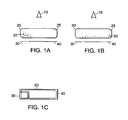
- FIG. 1A is a diagrammatic side view of an embodiment of a rear-addressing electrode structure for a particle-based display in which the smaller electrode has been placed at a voltage relative to the large electrode causing the particles to migrate to the smaller electrode.
- FIG. 1B is a diagrammatic side view of an embodiment of a rear-addressing electrode structure for a particle-based display in which the larger electrode has been placed at a voltage relative to the smaller electrode causing the particles to migrate to the larger electrode.
- FIG. 1C is a diagrammatic top-down view of one embodiment of a rear-addressing electrode structure.
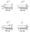
- FIG. 2A is a diagrammatic side view of an embodiment of a rear-addressing electrode structure having a retroreflective layer associated with the larger electrode in which the smaller electrode has been placed at a voltage relative to the large electrode causing the particles to migrate to the smaller electrode.
- FIG. 2B is a diagrammatic side view of an embodiment of a rear-addressing electrode structure having a retroreflective layer assoc iated with the larger electrode in which the larger electrode has been placed at a voltage relative to the smaller electrode causing the particles to migrate to the larger electrode.
- FIG. 2C is a diagrammatic side view of an embodiment of a rear-addressing electrode structure having a retroreflective layer disposed below the larger electrode in which the smaller electrode has been placed at a voltage relative to the large electrode causing the particles to migrate to the smaller electrode.
- FIG. 2D is a diagrammatic side view of an embodiment of a rear-addressing electrode structure having a retroreflective layer disposed below the larger electrode in which the larger electrode has been placed at a voltage relative to the smaller electrode causing the particles to migrate to the larger electrode.
- FIG. 3A is a diagrammatic side view of an embodiment of an addressing structure in which a direct-current electric field has been applied to the capsule causing the particles to migrate to the smaller electrode.
- FIG. 3B is a diagrammatic side view of an embodiment of an addressing structure in which an alternating-current electric field has been applied to the capsule causing the particles to disperse into the capsule.
- FIG. 3C is a diagrammatic side view of an embodiment of an addressing structure having transparent electrodes, in which a direct-current electric field has been applied to the capsule causing the particles to migrate to the smaller electrode.
- FIG. 3D is a diagrammatic side view of an embodiment of an addressing structure having transparent electrodes, in which an alternating-current electric field has been applied to the capsule causing the particles to disperse into the capsule.
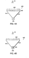
- FIG. 4A is a diagrammatic cross-sectional view of a shutter mode display element in a light-blocking configuration.
- FIG. 4B is a diagrammatic cross-sectional view of a shutter mode display element in a light-passing configuration.
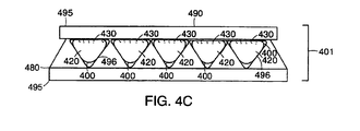
- FIG. 4C is a diagrammatic side view of a display formed of multiple shutter mode display elements.
- An electronic ink is an optoelectronically active material which comprises at least two phases: an electrophoretic contrast media phase and a coating/binding phase.
- the electrophoretic phase comprises, in some embodiments, a single species of electrophoretic particles dispersed in a clear or dyed medium, or more than one species of electrophoretic particles having distinct physical and electrical characteristics dispersed in a clear or dyed medium.
- the electrophoretic phase is encapsulated, that is, there is a capsule wall phase between the two phases.
- the coating/binding phase includes, in one embodiment, a polymer matrix that surrounds the electrophoretic phase.
- the polymer in the polymeric binder is capable of being dried, crosslinked, or otherwise cured as in traditional inks, and therefore a printing process can be used to deposit the electronic ink onto a substrate.
- An electronic ink is capable of being printed by several different processes, depending on the mechanical properties of the specific ink employed. For example, the fragility or viscosity of a particular ink may result in a different process selection. A very viscous ink would not be well-suited to deposition by an inkjet printing process, while a fragile ink might not be used in a knife over roll coating process.
- the optical quality of an electronic ink is quite distinct from other electronic display materials.
- the most notable difference is that the electronic ink provides a high degree of both reflectance and contrast because it is pigment based (as are ordinary printing inks).
- the light scattered from the electronic ink comes from a very thin layer of pigment close to the top of the viewing surface. In this respect it resembles an ordinary, printed image.
- electronic ink is easily viewed from a wide range of viewing angles in the same manner as a printed page, and such ink approximates a Lambertian contrast curve more closely than any other electronic display material. Since electronic ink can be printed, it can be included on the same surface with any other printed material, including traditional inks.
- Electronic ink can be made optically stable in all display configurations, that is, the ink can be set to a persistent optical state. Fabrication of a display by printing an electronic ink is particularly useful in low power applications because of this stability.
- Electronic ink displays are novel in that they can be addressed by DC voltages and draw very little current.
- the conductive leads and electrodes used to deliver the voltage to electronic ink displays can be of relatively high resistivity.
- the ability to use resistive conductors substantially widens the number and type of materials that can be used as conductors in electronic ink displays.
- ITO indium tin oxide
- the use of costly vacuum-sputtered indium tin oxide (ITO) conductors a standard material in liquid crystal devices, is not required.
- the replacement of ITO with other materials can provide benefits in appearance, processing capabilities (printed conductors), flexibility, and durability.
- the printed electrodes are in contact only with a solid binder, not with a fluid layer (like liquid crystals).
- conductive materials which would otherwise dissolve or be degraded by contact with liquid crystals, can be used in an electronic ink application.
- These conductive coatings include semiconducting colloids, examples of which are indium tin oxide and antimony-doped tin oxide.
- Organic conductors polymeric conductors and molecular organic conductors also may be used.
- Polymers include, but are not limited to, polyaniline and derivatives, polythiophene and derivatives, poly3,4-ethylenedioxythiophene (PEDOT) and derivatives, polypyrrole and derivatives, and polyphenylenevinylene (PPV) and derivatives.
- Organic molecular conductors include, but are not limited to, derivatives of naphthalene, phthalocyanine, and pentacene.
- Polymer layers can be made thinner and more transparent than with traditional displays because conductivity requirements are not as stringent.
- electroconductive powders which are also useful as coatable transparent conductors in electronic ink displays.
- electroconductive powders which are also useful as coatable transparent conductors in electronic ink displays.
- Zelec ECP electroconductive powders from DuPont Chemical Co. of Wilmington, Delaware.
- FIGs. 1A and 1B an addressing scheme for controlling particle-based displays is shown in which electrodes are disposed on only one side of a display, allowing the display to be rear-addressed. Utilizing only one side of the display for electrodes simplifies fabrication of displays. For example, if the electrodes are disposed on only the rear side of a display, both of the electrodes can be fabricated using opaque materials, because the electrodes do not need to be transparent.
- FIG. 1A depicts a single capsule 20 of an encapsulated display media.
- the embodiment depicted in FIG. 1A includes a capsule 20 containing at least one particle 50 dispersed in a suspending fluid 25.
- the capsule 20 is addressed by a first electrode 30 and a second electrode 40.
- the first electrode 30 is smaller than the second electrode 40.
- the first electrode 30 and the second electrode 40 may be set to voltage potentials which affect the position of the particles 50 in the capsule 20.
- the particles 50 represent 0.1% to 20% of the volume enclosed by the capsule 20. In some embodiments the particles 50 represent 2.5% to 17.5% of the volume enclosed by capsule 20. In preferred embodiments, the particles 50 represent 5% to 15% of the volume enclosed by the capsule 20. In more preferred embodiments the particles 50 represent 9% to 11% of the volume defined by the capsule 20. In general, the volume percentage of the capsule 20 that the particles 50 represent should be selected so that the particles 50 expose most of the second, larger electrode 40 when positioned over the first, smaller electrode 30. As described in detail below, the particles 50 may be colored any one of a number of colors. The particles 50 may be either positively charged or negatively charged.
- the particles 50 are dispersed in a dispersing fluid 25.
- the dispersing fluid 25 should have a low dielectric constant.
- the fluid 25 may be clear, or substantially clear, so that the fluid 25 does not inhibit viewing the particles 50 and the electrodes 30, 40 from position 10.
- the fluid 25 is dyed.
- the dispersing fluid 25 has a specific gravity matched to the density of the particles 50. These embodiments can provide a bistable display media, because the particles 50 do not tend to move in certain compositions absent an electric field applied via the electrodes 30, 40.
- the electrodes 30, 40 should be sized and positioned appropriately so that together they address the entire capsule 20. There may be exactly one pair of electrodes 30, 40 per capsule 20 multiple pairs of electrodes 30, 40 per capsule 20, or a single pair of electrodes 30, 40 may span multiple capsules 20. In the embodiment shown in FIGs. 1A and 1B , the capsule 20 has a flattened, rectangular shape. In these embodiments, the electrodes 30, 40 should address most, or all, of the flattened surface area adjacent the electrodes 30, 40.
- the smaller electrode 30 is at most one-half the size of the larger electrode 40. In preferred embodiments the smaller electrode is one-quarter the size of the larger electrode 40; in more preferred embodiments the smaller electrode 30 is one-eighth the size of the larger electrode 40.
- the smaller electrode 30 is one-sixteenth the size of the larger electrode 40. It should be noted that reference to "smaller” in connection with the electrode 30 means that the electrode 30 addresses a smaller amount of the surface area of the capsule 20, not necessarily that the electrode 30 is physically smaller than the larger electrode 40. For example, multiple capsules 20 may be positioned such that less of each capsule 20 is addressed by the "smaller" electrode 30, even though both electrodes 30, 40 are equal in size. It should also be noted that, as shown in FIG. 1C , electrode 30 may address only a small corner of a rectangular capsule 20 (shown in phantom view in FIG. 1C ), requiring the larger electrode 40 to surround the smaller electrode 30 on two sides in order to properly address the capsule 20. Selection of the percentage volume of the particles 50 and the electrodes 30, 40 in this manner allow the encapsulated display media to be addressed as described below.
- Electrodes may be fabricated from any material capable of conducting electricity so that electrode 30, 40 may apply an electric field to the capsule 20.
- the rear-addressed embodiments depicted in FIGs. 1A and 1B allow the electrodes 30, 40 to be fabricated from opaque materials such as solder paste, copper, copper-clad polyimide, graphite inks, silver inks and other metal-containing conductive inks.
- electrodes may be fabricated using transparent materials such as indium tin oxide and conductive polymers such as polyaniline or polythiopenes.
- Electrodes 30, 40 may be provided with contrasting optical properties. In some embodiments, one of the electrodes has an optical property complementary to optical properties of the particles 50.
- the capsule 20 contains positively charged black particles 50, and a substantially clear suspending fluid 25.
- the first, smaller electrode 30 is colored black, and is smaller than the second electrode 40, which is colored white or is highly reflective.
- the smaller, black electrode 30 is placed at a negative voltage potential relative to larger, white electrode 40, the positively-charged particles 50 migrate to the smaller, black electrode 30.
- the effect to a viewer of the capsule 20 located at position 10 is a mixture of the larger, white electrode 40 and the smaller, black electrode 30, creating an effect which is largely white. Referring to FIG.
- the capsule 20 may be addressed to display either a white visual state or a black visual state.
- varying the color of the smaller electrode 30 and the particles 50 allows fabrication of a rear-addressed, two-color display having black as one of the colors.
- varying the color of the smaller electrode 30 and the particles 50 allow a rear-addressed two-color system to be fabricated having white as one of the colors.
- the particles 50 and the smaller electrode 30 can be different colors.
- a two-color display may be fabricated having a second color that is different from the color of the smaller electrode 30 and the particles 50.
- a rear-addressed, orange-white display may be fabricated by providing blue particles 50, a red, smaller electrode 30, and a white (or highly reflective) larger electrode 40.
- the optical properties of the electrodes 30, 40 and the particles 50 can be independently selected to provide desired display characteristics.
- the optical properties of the dispersing fluid 25 may also be varied, e.g. the fluid 25 may be dyed.
- the larger electrode 40 may be reflective instead of white.
- the particles 50 when the particles 50 are moved to the smaller electrode 30, light reflects off the reflective surface 60 associated with the larger electrode 40 and the capsule 20 appears light in color, e.g. white (see FIG. 2A ).
- the reflecting surface 60 is obscured and the capsule 20 appears dark (see FIG. 2B ) because light is absorbed by the particles 50 before reaching the reflecting surface 60.
- the reflecting surface 60 for the larger electrode 40 may possess retroreflective properties, specular reflection properties, diffuse reflective properties or gain reflection properties.
- the reflective surface 60 reflects light with a Lambertian distribution.
- the surface 60 may be provided as a plurality of glass spheres disposed on the electrode 40, a diffractive reflecting layer such as a holographically formed reflector, a surface patterned to totally internally reflect incident light, a brightness-enhancing film, a diffuse reflecting layer, an embossed plastic or metal film, or any other known reflecting surface.
- the reflecting surface 60 may be provided as a separate layer laminated onto the larger electrode 40 or the reflecting surface 60 may be provided as a unitary part of the larger electrode 40.
- the reflecting surface may be disposed below the electrodes 30, 40 vis-à-vis the viewpoint 10.
- electrode 30 should be transparent so that light may be reflected by surface 60.
- proper switching of the particles may be accomplished with a combination of alternating-current (AC) and direct-current (DC) electric fields and described below in connection with FIGs. 3A-3D .
- the rear-addressed display previously discussed can be configured to transition between largely transmissive and largely opaque modes of operation (referred to hereafter as "shutter mode").
- the capsule 20 contains at least one positively-charged particle 50 dispersed in a substantially clear dispersing fluid 25.
- the larger electrode 40 is transparent and the smaller electrode 30 is opaque.
- the smaller, opaque electrode 30 is placed at a negative voltage potential relative to the larger, transmissive electrode 40, the particles 50 migrate to the smaller, opaque electrode 30.
- the effect to a viewer of the capsule 20 located at position 10 is a mixture of the larger, transparent electrode 40 and the smaller, opaque electrode 30, creating an effect which is largely transparent. Referring to FIG.
- FIGs. 1A-2D depict a pair of electrodes associated with each capsule 20, it should be understood that each pair of electrodes may be associated with more than one capsule 20.
- a capsule 20 contains at least one dark or black particle 50 dispersed in a substantially clear dispersing fluid 25.
- a smaller, opaque electrode 30 and a larger, transparent electrode 40 apply both direct-current (DC) electric fields and alternating-current (AC) fields to the capsule 20.
- a DC field can be applied to the capsule 20 to cause the particles 50 to migrate towards the smaller electrode 30. For example, if the particles 50 are positively charged, the smaller electrode is placed a voltage that is more negative than the larger electrode 40.
- FIGs. 3A-3D depict only one capsule per electrode pair, multiple capsules may be addressed using the same electrode pair.
- the smaller electrode 30 is at most one-half the size of the larger electrode 40. In preferred embodiments the smaller electrode is one-quarter the size of the larger electrode 40; in more preferred embodiments the smaller electrode 30 is one-eighth the size of the larger electrode 40. In even more preferred embodiments, the smaller electrode 30 is one-sixteenth the size of the larger electrode 40.
- Causing the particles 50 to migrate to the smaller electrode 30, as depicted in FIG. 3A allows incident light to pass through the larger, transparent electrode 40 and be reflected by a reflecting surface 60.
- the reflecting surface 60 is replaced by a translucent layer, a transparent layer, or a layer is not provided at all, and incident light is allowed to pass through the capsule 20, i.e. the capsule 20 is transmissive.
- the particles 50 are dispersed into the capsule 20 by applying an AC field to the capsule 20 via the electrodes 30, 40.
- the particles 50, dispersed into the capsule 20 by the AC field block incident light from passing through the capsule 20, causing it to appear dark at the viewpoint 10.
- the embodiment depicted in FIGs. 3A-3B may be used in shutter mode by not providing the reflecting surface 60 and instead providing a translucent layer, a transparent layer, or no layer at all. In shutter mode, application of an AC electric field causes the capsule 20 to appear opaque.
- the transparency of a shutter mode display formed by the apparatus depicted in FIGs. 3A-3D may be controlled by the number of capsules addressed using DC fields and AC fields. For example, a display in which every other capsule 20 is addressed using an AC field would appear fifty percent transmissive.
- FIGs. 3C and 3D depict an embodiment of the electrode structure described above in which electrodes 30, 40 are on "top" of the capsule 20, that is, the electrodes 30, 40 are between the viewpoint 10 and the capsule 20.
- both electrodes 30, 40 should be transparent.
- Transparent polymers can be fabricated using conductive polymers, such as polyaniline, polythiophenes, or indium tin oxide. These materials may be made soluble so that electrodes can be fabricated using coating techniques such as spin coating, spray coating, meniscus coating, printing techniques, forward and reverse roll coating and the like.
- light passes through the electrodes 30, 40 and is either absorbed by the particles 50, reflected by retroreflecting layer 60 (when provided), or transmitted throughout the capsule 20 (when retroreflecting layer 60 is not provided).
- FIGs. 3A-3D depict embodiments in which electrode 30, 40 are statically attached to the display media.
- the particles 50 exhibit bistability, that is, they are substantially motionless in the absence of a electric field.
- the electrodes 30, 40 may be provided as part of a "stylus" or other device which is scanned over the material to address each capsule or cluster of capsules.
- FIG. 4A depicts a cross-sectional side view of an embodiment of a shutter mode encapsulated electrophoretic display element 400 in its light-blocking configuration.
- the element comprises a microcapsule 410, which contains a suspending fluid 420 and at least one particle 430.
- the microcapsule 410 has a first, larger surface 440 and a second, smaller surface 450.
- the microcapsule is subjected to a first electric field of such an orientation and strength that the particles 430 migrate towards the larger surface 440, substantially blocking light from passing through the microcapsule 410 when the particles 430 are substantially opaque.
- the particles 430 have positive charge, the particles will migrate towards the larger surface 440 when an electric field having an electric vector with a positive gradient extending substantially from the larger surface 440 to the smaller surface 450 is applied, that is, an electric field is applied which has a more negative voltage at the larger surface 440 and a more positive voltage at the smaller surface 450.
- the element would appear to a viewer 10 to have the optical property or properties of the particles 430.
- the particles 430 may be colored.
- the electrophoretic display element 400 exhibit the color of the particles 430.
- the particles 430 are reflective, and the electrophoretic display element 400 will appear reflective. It will be apparent to those of ordinary skill in the art that the visual appearance of the electrophoretic display element 400 may be varied by selecting the visual appearance of the particles 430 appropriately.
- the electrophoretic display element 400 has a substantially triangular cross section, as depicted in FIG. 4A .
- An electrophoretic display element 400 having such a cross section may be substantially conical or substantially pyramidal in shape.
- the electrophoretic display element 400 may have a substantially trapezoidal cross-section.
- the electrophoretic display element 400 may have a substantially rectangular cross section.
- the electrophoretic display element 400 can have a shape which is not regular, provided that the second surface 450 is smaller than the first surface 440.
- FIG. 4B depicts a cross-sectional side view of an embodiment of a shutter mode encapsulated electrophoretic display element 400 in its light-passing configuration.
- the element comprises a microcapsule 410, which contains a suspending fluid 420 and at least one particle 430.
- the microcapsule has a first, larger surface 440 and a second, smaller surface 450.
- the microcapsule is subjected to a second electric field of such an orientation and strength that the particles 430 migrates towards the smaller surface 450, allowing light to pass through the microcapsule 410 because the particles are concentrated in a vary small area of the microcapsule.
- the element 410 would appear to a viewer 10 to have the optical property or properties of the suspending fluid 420.
- the suspending fluid 420 is clear, and the electrophoretic display element 400 will appear substantially transparent.
- the suspending fluid 420 may be dyed or may inherently be colored, and the electrophoretic display element 400 will present to the viewer 10 the color of the fluid 420.
- an electrode may be provided behind the electrophoretic display element 400 that is colored, or a substrate may be present having a color. In these embodiments, the electrophoretic display element 400 will present a visual appearance that is a function of both the optical characteristic of the electrode or substrate and the suspending fluid 420.
- the second, smaller surface 450 may be 90% of the area of the first larger surface 440. In another embodiment the area of the second, smaller surface 450 may be 80% of the area of the first larger surface 440. In yet another embodiment the area of the second, smaller surface 450 may be 70% of the area of the first larger surface 440. In still another embodiment the area of the second, smaller surface 450 may be 60% of the area of the first larger surface 440. In a further embodiment the area of the second, smaller surface 450 may be 50% of the area of the first larger surface 440. In yet a further embodiment the area of the second, smaller surface 450 may be 25% of the area of the first larger surface 440. In a still further embodiment the area of the second, smaller surface 450 may be 12.5% of the area of the first larger surface 440. In another embodiment the area of the second, smaller surface 450 may be 1/16th of the area of the first larger surface 440.
- FIG. 4C depicts a side view of an embodiment of a plurality of shutter mode electrophoretic display elements, generally 400, which have been arranged as an electrophoretic display 401.
- the electrophoretic display elements 400 are controlled as described above in connection with FIGs. 4A and 4B .
- the electrophoretic display 401 can be created by providing a first substrate 480 that forms a number of cavities. In the embodiment depicted in FIG. 4C , each cavity has a triangular cross-section in the substrate, such as a conical depression, a pyramidal depression or a groove having a triangular cross section.
- a second substrate 490 may be attached to the first substrate to close each of the cavities.
- Electrodes 495 may be disposed adjacent the substrates to apply an electric field to the display elements 400.
- electrodes 496 may be disposed on at least a part of the surface of the first substrate 480 that defines the cavities, so that an electric field can be applied to the display elements 400 in an orientation which is oblique, rather than perpendicular, to the surface of the first substrate 480.
- the first substrate 480 can provide cavities having trapezoidal, conic, or hemispheric cross-sections. In other embodiments, the first substrate 480 provides cavities having cross-sections that are not geometrically regular. Alternatively, the first substrate 480 may provide a substantially planar surfaces defining a trough having a triangular cross section. Alternatively, the trough can be substantially straight, curvilinear (such as a spiral), a series of concentric circular troughs, or grooves having substantially parallel sides. As can be appreciated by those of ordinary skill in the art, many different shapes of cavities may be used with success. The cavities may be provided in a regular arrangement, such as a rectangular grid, or the cavities may be irregularly spaced.
- the first substrate 480 is substantially clear.
- the electrophoretic display 401 is substantially transparent when the display elements 400 are in the light-passing configuration.
- the display 401 will have the optical characteristics of the plurality of particles 430 when the display elements 400 are in the light-blocking configuration.
- the first substrate 480 can be colored.
- the electrophoretic display 401 will appear substantially colored when the display elements 400 are in the light passing configuration.
- the display 401 will have substantially the optical characteristics of the plurality of particles 430 when the display elements 400 are in the light-blocking configuration.
- the suspending fluid 420 can be colored, and the electrophoretic display 401 will have the same color as the suspending fluid 420 when the display elements 400 are in the light passing configuration.
- the display 401 will have substantially the optical characteristics of the plurality of particles 430 when the display elements 400 are in the light-blocking configuration.
- the first substrate 480 can be patterned by etching, by micromachining, or by embossing using a suitable embossing die or by other pressure or thermal processes.
- Organic solvents such as halogenated organic solvents, saturated linear or branched hydrocarbons, silicone oils, and low molecular weight halogen-containing polymers are some useful suspending fluids.
- the suspending fluid may comprise a single fluid.
- the fluid will, however, often be a blend of more than one fluid in order to tune its chemical and physical properties.
- the fluid may contain surface modifiers to modify the surface energy or charge of the electrophoretic particle or bounding capsule.
- Reactants or solvents for the microencapsulation process oil soluble monomers, for example
- Charge control agents can also be added to the suspending fluid.
- Useful organic solvents include, but are not limited to, epoxides, such as, for example, decane epoxide and dodecane epoxide; vinyl ethers, such as, for example, cyclohexyl vinyl ether and Decave ® (International Flavors & Fragrances, Inc., New York, NY); and aromatic hydrocarbons, such as, for example, toluene and naphthalene.
- Useful halogenated organic solvents include, but are not limited to, tetrafluorodibromoethylene, tetrachloroethylene, trifluorochloroethylene, 1,2,4-trichlorobenzene, carbon tetrachloride. These materials have high densities.
- Useful hydrocarbons include, but are not limited to, dodecane, tetradecane, the aliphatic hydrocarbons in the Isopar ® series (Exxon, Houston, TX), Norpar ® ( series of normal paraffinic liquids), Shell-Sol ® (Shell, Houston, TX), and Sol-Trol ® (Shell), naphtha, and other petroleum solvents. These materials usually have low densities.
- Useful examples of silicone oils include, but are not limited to, octamethyl cyclosiloxane and higher molecular weight cyclic siloxanes, poly (methyl phenyl siloxane), hexamethyldisiloxane, and polydimethylsiloxane.
- Useful low molecular weight halogen-containing polymers include, but are not limited to, poly(chlorotrifluoroethylene) polymer (Halogenated hydrocarbon Inc., River Edge, NJ), Galden ® (a perfluorinated ether from Ausimont, Morristown, NJ), or Krytox ® from Dupont (Wilmington, DE).
- the suspending fluid is a poly(chlorotrifluoroethylene) polymer.
- this polymer has a degree of polymerization from about 2 to about 10. Many of the above materials are available in a range of viscosities, densities, and boiling points.
Landscapes
- Physics & Mathematics (AREA)
- Nonlinear Science (AREA)
- General Physics & Mathematics (AREA)
- Optics & Photonics (AREA)
- Engineering & Computer Science (AREA)
- Life Sciences & Earth Sciences (AREA)
- Chemical & Material Sciences (AREA)
- Theoretical Computer Science (AREA)
- Health & Medical Sciences (AREA)
- Molecular Biology (AREA)
- Electrochemistry (AREA)
- Chemical Kinetics & Catalysis (AREA)
- Mathematical Physics (AREA)
- Crystallography & Structural Chemistry (AREA)
- Electrochromic Elements, Electrophoresis, Or Variable Reflection Or Absorption Elements (AREA)
- Devices For Indicating Variable Information By Combining Individual Elements (AREA)
Description
- The present invention relates to encapsulated electrophoretic displays and, in particular, to shutter mode encapsulated electrophoretic displays.
- Traditionally, electronic displays such as liquid crystal displays have been made by sandwiching an optoelectrically active material between two pieces of glass. In many cases each piece of glass has an etched, clear electrode structure formed using indium tin oxide. A first electrode structure controls all the segments of the display that may be addressed, that is, changed from one visual state to another. A second electrode, sometimes called a counter electrode, addresses all display segments as one large electrode, and is generally designed not to overlap any of the rear electrode wire connections that are not desired in the final image. Alternatively, the second electrode is also patterned to control specific segments of the display. In these displays, unaddressed areas of the display have a defined appearance.
- Electrophoretic display media, generally characterized by the movement of particles through an applied electric field, are highly reflective, can be made bistable, and consume very little power. Encapsulated electrophoretic displays also enable the display to be printed. These properties allow encapsulated electrophoretic display media to be used in many applications for which traditional electronic displays are not suitable, such as flexible displays. The electro-optical properties of encapsulated displays allow, and in some cases require, novel schemes or configurations to be used to address the displays.
- "Shutter mode" electrophoretic displays are configured so that the particles can switch between a largely light-blocking (or reflecting) state and a largely light-transmitting state. These displays often are constructed with particles which can migrate between a smaller and larger electrode. Migration of the particles to the large electrodes allows them to spread out, causing the capsule to take on the visual properties of the particles. Migration of the particles to the smaller electrode causes the capsule to take on the visual properties of the dispersing fluid or of the larger electrode, because the particles are "clumped" together near the smaller electrode. Another use of this effect is to control transmission of light through the capsule. The drawback to shutter mode displays is that the electrodes must be etched very precisely.
- This invention seeks to provide a highly-flexible, reflective display which can be manufactured easily, consumes little (or none in the case of bistable displays) power, and can, therefore, be incorporated into a variety of applications. The invention may be in form of a printable display comprising an encapsulated electrophoretic display medium. The resulting display may be flexible. Since the display media can be printed, the display itself can be made inexpensively. In particular, the present invention allows shutter mode electrophoretic displays to be fabricated without requiring finely etched electrodes.
- An encapsulated electrophoretic display can be constructed so that the optical state of the display is stable for some length of time. When the display has two states which are stable in this manner, the display is said to be bistable. If more than two states of the display are stable, then the display can be said to be multistable. For the purpose of this invention, the term bistable will be used to indicate a display in which any optical state remains fixed once the addressing voltage is removed. The definition of a bistable state depends on the application for the display. A slowly-decaying optical state can be effectively bistable if the optical state is substantially unchanged over the required viewing time. For example, in a display which is updated every few minutes, a display image which is stable for hours or days is effectively bistable for that application. In this invention, the term bistable also indicates a display with an optical state sufficiently long-lived as to be effectively bistable for the application in mind. Alternatively, it is possible to construct encapsulated electrophoretic displays in which the image decays quickly once the addressing voltage to the display is removed (i.e., the display is not bistable or multistable). As will be described, in some applications it is advantageous to use an encapsulated electrophoretic display which is not bistable. Whether or not an encapsulated electrophoretic display is bistable, and its degree of bistability, can be controlled through appropriate chemical modification of the electrophoretic particles, the suspending fluid, the capsule, and binder materials.
- An encapsulated electrophoretic display may take many forms. The display comprises capsules. The capsules may be of any size or shape. The capsules are formed by an encapsulation technique, as described below. Particles are encapsulated in the capsules. The particles may be one or more different types of particles. The particles may be colored, luminescent, light-absorbing or transparent, for example. The particles may include neat pigments, dyed (laked) pigments or pigment/polymer composites, for example. The capsules further comprise a suspending fluid in which the particles are dispersed.
- The successful construction of an encapsulated electrophoretic display requires the proper interaction of several different types of materials and processes, such as a polymeric binder and, optionally, a capsule membrane. These materials must be chemically compatible with the electrophoretic particles and fluid, as well as with each other. The capsule materials may engage in useful surface interactions with the electrophoretic particles, or may act as a chemical or physical boundary between the fluid and the binder.
- Throughout the specification, reference will be made to printing or printed. As used throughout the specification, printing is intended to include all forms of printing and coating, including: premetered coatings such as patch die coating, slot or extrusion coating, slide or cascade coating, and curtain coating; roll coating such as knife over roll coating, forward and reverse roll coating; gravure coating; dip coating; spray coating; meniscus coating; spin coating; brush coating; air knife coating; silk screen printing processes; electrostatic printing processes; thermal printing processes; and other similar techniques. A "printed element" refers to an element formed using any one of the above techniques.
-
JP-A-04-345133 - In one aspect, the invention provides an encapsulated electrophoretic display which resembles that described in
JP-A-04-345133 - The invention is pointed out with particularity in the appended claims. The advantages of the invention described above, together with further advantages, may be better understood by referring to the following description taken in conjunction with the accompanying drawings. In the drawings, like reference characters generally refer to the same parts throughout the different views. Also, the drawings are not necessarily to scale, emphasis instead generally being placed upon illustrating the principles of the invention.
-
FIG. 1A is a diagrammatic side view of an embodiment of a rear-addressing electrode structure for a particle-based display in which the smaller electrode has been placed at a voltage relative to the large electrode causing the particles to migrate to the smaller electrode. -
FIG. 1B is a diagrammatic side view of an embodiment of a rear-addressing electrode structure for a particle-based display in which the larger electrode has been placed at a voltage relative to the smaller electrode causing the particles to migrate to the larger electrode. -
FIG. 1C is a diagrammatic top-down view of one embodiment of a rear-addressing electrode structure. -
FIG. 2A is a diagrammatic side view of an embodiment of a rear-addressing electrode structure having a retroreflective layer associated with the larger electrode in which the smaller electrode has been placed at a voltage relative to the large electrode causing the particles to migrate to the smaller electrode. -
FIG. 2B is a diagrammatic side view of an embodiment of a rear-addressing electrode structure having a retroreflective layer assoc iated with the larger electrode in which the larger electrode has been placed at a voltage relative to the smaller electrode causing the particles to migrate to the larger electrode. -
FIG. 2C is a diagrammatic side view of an embodiment of a rear-addressing electrode structure having a retroreflective layer disposed below the larger electrode in which the smaller electrode has been placed at a voltage relative to the large electrode causing the particles to migrate to the smaller electrode. -
FIG. 2D is a diagrammatic side view of an embodiment of a rear-addressing electrode structure having a retroreflective layer disposed below the larger electrode in which the larger electrode has been placed at a voltage relative to the smaller electrode causing the particles to migrate to the larger electrode. -
FIG. 3A is a diagrammatic side view of an embodiment of an addressing structure in which a direct-current electric field has been applied to the capsule causing the particles to migrate to the smaller electrode. -
FIG. 3B is a diagrammatic side view of an embodiment of an addressing structure in which an alternating-current electric field has been applied to the capsule causing the particles to disperse into the capsule. -
FIG. 3C is a diagrammatic side view of an embodiment of an addressing structure having transparent electrodes, in which a direct-current electric field has been applied to the capsule causing the particles to migrate to the smaller electrode. -
FIG. 3D is a diagrammatic side view of an embodiment of an addressing structure having transparent electrodes, in which an alternating-current electric field has been applied to the capsule causing the particles to disperse into the capsule. -
FIG. 4A is a diagrammatic cross-sectional view of a shutter mode display element in a light-blocking configuration. -
FIG. 4B is a diagrammatic cross-sectional view of a shutter mode display element in a light-passing configuration. -
FIG. 4C is a diagrammatic side view of a display formed of multiple shutter mode display elements. - An electronic ink is an optoelectronically active material which comprises at least two phases: an electrophoretic contrast media phase and a coating/binding phase. The electrophoretic phase comprises, in some embodiments, a single species of electrophoretic particles dispersed in a clear or dyed medium, or more than one species of electrophoretic particles having distinct physical and electrical characteristics dispersed in a clear or dyed medium. The electrophoretic phase is encapsulated, that is, there is a capsule wall phase between the two phases. The coating/binding phase includes, in one embodiment, a polymer matrix that surrounds the electrophoretic phase. In this embodiment, the polymer in the polymeric binder is capable of being dried, crosslinked, or otherwise cured as in traditional inks, and therefore a printing process can be used to deposit the electronic ink onto a substrate. An electronic ink is capable of being printed by several different processes, depending on the mechanical properties of the specific ink employed. For example, the fragility or viscosity of a particular ink may result in a different process selection. A very viscous ink would not be well-suited to deposition by an inkjet printing process, while a fragile ink might not be used in a knife over roll coating process.
- The optical quality of an electronic ink is quite distinct from other electronic display materials. The most notable difference is that the electronic ink provides a high degree of both reflectance and contrast because it is pigment based (as are ordinary printing inks). The light scattered from the electronic ink comes from a very thin layer of pigment close to the top of the viewing surface. In this respect it resembles an ordinary, printed image. Also, electronic ink is easily viewed from a wide range of viewing angles in the same manner as a printed page, and such ink approximates a Lambertian contrast curve more closely than any other electronic display material. Since electronic ink can be printed, it can be included on the same surface with any other printed material, including traditional inks. Electronic ink can be made optically stable in all display configurations, that is, the ink can be set to a persistent optical state. Fabrication of a display by printing an electronic ink is particularly useful in low power applications because of this stability.
- Electronic ink displays are novel in that they can be addressed by DC voltages and draw very little current. As such, the conductive leads and electrodes used to deliver the voltage to electronic ink displays can be of relatively high resistivity. The ability to use resistive conductors substantially widens the number and type of materials that can be used as conductors in electronic ink displays. In particular, the use of costly vacuum-sputtered indium tin oxide (ITO) conductors, a standard material in liquid crystal devices, is not required. Aside from cost savings, the replacement of ITO with other materials can provide benefits in appearance, processing capabilities (printed conductors), flexibility, and durability. Additionally, the printed electrodes are in contact only with a solid binder, not with a fluid layer (like liquid crystals). This means that some conductive materials, which would otherwise dissolve or be degraded by contact with liquid crystals, can be used in an electronic ink application. These include opaque metallic inks for the rear electrode (e.g., silver and graphite inks), as well as conductive transparent inks for either substrate. These conductive coatings include semiconducting colloids, examples of which are indium tin oxide and antimony-doped tin oxide. Organic conductors (polymeric conductors and molecular organic conductors) also may be used. Polymers include, but are not limited to, polyaniline and derivatives, polythiophene and derivatives, poly3,4-ethylenedioxythiophene (PEDOT) and derivatives, polypyrrole and derivatives, and polyphenylenevinylene (PPV) and derivatives. Organic molecular conductors include, but are not limited to, derivatives of naphthalene, phthalocyanine, and pentacene. Polymer layers can be made thinner and more transparent than with traditional displays because conductivity requirements are not as stringent.
- As an example, there are a class of materials called electroconductive powders which are also useful as coatable transparent conductors in electronic ink displays. One example is Zelec ECP electroconductive powders from DuPont Chemical Co. of Wilmington, Delaware.
- Referring now to
FIGs. 1A and 1B , an addressing scheme for controlling particle-based displays is shown in which electrodes are disposed on only one side of a display, allowing the display to be rear-addressed. Utilizing only one side of the display for electrodes simplifies fabrication of displays. For example, if the electrodes are disposed on only the rear side of a display, both of the electrodes can be fabricated using opaque materials, because the electrodes do not need to be transparent. -
FIG. 1A depicts asingle capsule 20 of an encapsulated display media. In brief overview, the embodiment depicted inFIG. 1A includes acapsule 20 containing at least oneparticle 50 dispersed in a suspendingfluid 25. Thecapsule 20 is addressed by afirst electrode 30 and asecond electrode 40. Thefirst electrode 30 is smaller than thesecond electrode 40. Thefirst electrode 30 and thesecond electrode 40 may be set to voltage potentials which affect the position of theparticles 50 in thecapsule 20. - The
particles 50 represent 0.1% to 20% of the volume enclosed by thecapsule 20. In some embodiments theparticles 50 represent 2.5% to 17.5% of the volume enclosed bycapsule 20. In preferred embodiments, theparticles 50 represent 5% to 15% of the volume enclosed by thecapsule 20. In more preferred embodiments theparticles 50 represent 9% to 11% of the volume defined by thecapsule 20. In general, the volume percentage of thecapsule 20 that theparticles 50 represent should be selected so that theparticles 50 expose most of the second,larger electrode 40 when positioned over the first,smaller electrode 30. As described in detail below, theparticles 50 may be colored any one of a number of colors. Theparticles 50 may be either positively charged or negatively charged. - The
particles 50 are dispersed in a dispersingfluid 25. The dispersingfluid 25 should have a low dielectric constant. The fluid 25 may be clear, or substantially clear, so that the fluid 25 does not inhibit viewing theparticles 50 and theelectrodes position 10. In other embodiments, the fluid 25 is dyed. In some embodiments the dispersingfluid 25 has a specific gravity matched to the density of theparticles 50. These embodiments can provide a bistable display media, because theparticles 50 do not tend to move in certain compositions absent an electric field applied via theelectrodes - The
electrodes entire capsule 20. There may be exactly one pair ofelectrodes capsule 20 multiple pairs ofelectrodes capsule 20, or a single pair ofelectrodes multiple capsules 20. In the embodiment shown inFIGs. 1A and 1B , thecapsule 20 has a flattened, rectangular shape. In these embodiments, theelectrodes electrodes smaller electrode 30 is at most one-half the size of thelarger electrode 40. In preferred embodiments the smaller electrode is one-quarter the size of thelarger electrode 40; in more preferred embodiments thesmaller electrode 30 is one-eighth the size of thelarger electrode 40. In even more preferred embodiments, thesmaller electrode 30 is one-sixteenth the size of thelarger electrode 40. It should be noted that reference to "smaller" in connection with theelectrode 30 means that theelectrode 30 addresses a smaller amount of the surface area of thecapsule 20, not necessarily that theelectrode 30 is physically smaller than thelarger electrode 40. For example,multiple capsules 20 may be positioned such that less of eachcapsule 20 is addressed by the "smaller"electrode 30, even though bothelectrodes FIG. 1C ,electrode 30 may address only a small corner of a rectangular capsule 20 (shown in phantom view inFIG. 1C ), requiring thelarger electrode 40 to surround thesmaller electrode 30 on two sides in order to properly address thecapsule 20. Selection of the percentage volume of theparticles 50 and theelectrodes - Electrodes may be fabricated from any material capable of conducting electricity so that
electrode capsule 20. As noted above, the rear-addressed embodiments depicted inFIGs. 1A and 1B allow theelectrodes Electrodes particles 50. - In one embodiment, the
capsule 20 contains positively chargedblack particles 50, and a substantially clear suspendingfluid 25. The first,smaller electrode 30 is colored black, and is smaller than thesecond electrode 40, which is colored white or is highly reflective. When the smaller,black electrode 30 is placed at a negative voltage potential relative to larger,white electrode 40, the positively-chargedparticles 50 migrate to the smaller,black electrode 30. The effect to a viewer of thecapsule 20 located atposition 10 is a mixture of the larger,white electrode 40 and the smaller,black electrode 30, creating an effect which is largely white. Referring toFIG. 1B , when the smaller,black electrode 30 is placed at a positive voltage potential relative to the larger,white electrode 40,particles 50 migrate to the larger,white electrode 40 and the viewer is presented a mixture of theblack particles 50 covering the larger,white electrode 40 and the smaller,black electrode 30, creating an effect which is largely black. In this manner thecapsule 20 may be addressed to display either a white visual state or a black visual state. - Other two-color schemes are easily provided by varying the color of the
smaller electrode 30 and theparticles 50 or by varying the color of thelarger electrode 40. For example, varying the color of thelarger electrode 40 allows fabrication of a rear-addressed, two-color display having black as one of the colors. Alternatively, varying the color of thesmaller electrode 30 and theparticles 50 allow a rear-addressed two-color system to be fabricated having white as one of the colors. Further, it is contemplated that theparticles 50 and thesmaller electrode 30 can be different colors. In these embodiments, a two-color display may be fabricated having a second color that is different from the color of thesmaller electrode 30 and theparticles 50. For example, a rear-addressed, orange-white display may be fabricated by providingblue particles 50, a red,smaller electrode 30, and a white (or highly reflective)larger electrode 40. In general, the optical properties of theelectrodes particles 50 can be independently selected to provide desired display characteristics. In some embodiments the optical properties of the dispersingfluid 25 may also be varied, e.g. the fluid 25 may be dyed. - In other embodiments the
larger electrode 40 may be reflective instead of white. In these embodiments, when theparticles 50 are moved to thesmaller electrode 30, light reflects off thereflective surface 60 associated with thelarger electrode 40 and thecapsule 20 appears light in color, e.g. white (seeFIG. 2A ). When theparticles 50 are moved to thelarger electrode 40, the reflectingsurface 60 is obscured and thecapsule 20 appears dark (seeFIG. 2B ) because light is absorbed by theparticles 50 before reaching the reflectingsurface 60. The reflectingsurface 60 for thelarger electrode 40 may possess retroreflective properties, specular reflection properties, diffuse reflective properties or gain reflection properties. In certain embodiments, thereflective surface 60 reflects light with a Lambertian distribution. Thesurface 60 may be provided as a plurality of glass spheres disposed on theelectrode 40, a diffractive reflecting layer such as a holographically formed reflector, a surface patterned to totally internally reflect incident light, a brightness-enhancing film, a diffuse reflecting layer, an embossed plastic or metal film, or any other known reflecting surface. The reflectingsurface 60 may be provided as a separate layer laminated onto thelarger electrode 40 or the reflectingsurface 60 may be provided as a unitary part of thelarger electrode 40. In the embodiments depicted byFIGs. 2C and 2D , the reflecting surface may be disposed below theelectrodes viewpoint 10. In these embodiments,electrode 30 should be transparent so that light may be reflected bysurface 60. In other embodiments, proper switching of the particles may be accomplished with a combination of alternating-current (AC) and direct-current (DC) electric fields and described below in connection withFIGs. 3A-3D . - In still other embodiments, the rear-addressed display previously discussed can be configured to transition between largely transmissive and largely opaque modes of operation (referred to hereafter as "shutter mode"). Referring back to
FIGs. 1A and 1B , in these embodiments thecapsule 20 contains at least one positively-chargedparticle 50 dispersed in a substantially clear dispersingfluid 25. Thelarger electrode 40 is transparent and thesmaller electrode 30 is opaque. When the smaller,opaque electrode 30 is placed at a negative voltage potential relative to the larger,transmissive electrode 40, theparticles 50 migrate to the smaller,opaque electrode 30. The effect to a viewer of thecapsule 20 located atposition 10 is a mixture of the larger,transparent electrode 40 and the smaller,opaque electrode 30, creating an effect which is largely transparent. Referring toFIG. 1B , when the smaller,opaque electrode 30 is placed at a positive voltage potential relative to the larger,transparent electrode 40,particles 50 migrate to thesecond electrode 40 and the viewer is presented a mixture of theopaque particles 50 covering the larger,transparent electrode 40 and the smaller,opaque electrode 30, creating an effect which is largely opaque. In this manner, a display formed using the capsules depicted inFIGs. 1A and 1B may be switched between transmissive and opaque modes. Such a display can be used to construct a window that can be rendered opaque. AlthoughFIGs. 1A-2D depict a pair of electrodes associated with eachcapsule 20, it should be understood that each pair of electrodes may be associated with more than onecapsule 20. - A similar technique may be used in connection with the embodiment of
FIGs. 3A, 3B, 3C, and 3D . Referring toFIG. 3A , acapsule 20 contains at least one dark orblack particle 50 dispersed in a substantially clear dispersingfluid 25. A smaller,opaque electrode 30 and a larger,transparent electrode 40 apply both direct-current (DC) electric fields and alternating-current (AC) fields to thecapsule 20. A DC field can be applied to thecapsule 20 to cause theparticles 50 to migrate towards thesmaller electrode 30. For example, if theparticles 50 are positively charged, the smaller electrode is placed a voltage that is more negative than thelarger electrode 40. AlthoughFIGs. 3A-3D depict only one capsule per electrode pair, multiple capsules may be addressed using the same electrode pair. - The
smaller electrode 30 is at most one-half the size of thelarger electrode 40. In preferred embodiments the smaller electrode is one-quarter the size of thelarger electrode 40; in more preferred embodiments thesmaller electrode 30 is one-eighth the size of thelarger electrode 40. In even more preferred embodiments, thesmaller electrode 30 is one-sixteenth the size of thelarger electrode 40. - Causing the
particles 50 to migrate to thesmaller electrode 30, as depicted inFIG. 3A , allows incident light to pass through the larger,transparent electrode 40 and be reflected by a reflectingsurface 60. In shutter mode, the reflectingsurface 60 is replaced by a translucent layer, a transparent layer, or a layer is not provided at all, and incident light is allowed to pass through thecapsule 20, i.e. thecapsule 20 is transmissive. - Referring now to
FIG. 3B , theparticles 50 are dispersed into thecapsule 20 by applying an AC field to thecapsule 20 via theelectrodes particles 50, dispersed into thecapsule 20 by the AC field, block incident light from passing through thecapsule 20, causing it to appear dark at theviewpoint 10. The embodiment depicted inFIGs. 3A-3B may be used in shutter mode by not providing the reflectingsurface 60 and instead providing a translucent layer, a transparent layer, or no layer at all. In shutter mode, application of an AC electric field causes thecapsule 20 to appear opaque. The transparency of a shutter mode display formed by the apparatus depicted inFIGs. 3A-3D may be controlled by the number of capsules addressed using DC fields and AC fields. For example, a display in which everyother capsule 20 is addressed using an AC field would appear fifty percent transmissive. -
FIGs. 3C and 3D depict an embodiment of the electrode structure described above in whichelectrodes capsule 20, that is, theelectrodes viewpoint 10 and thecapsule 20. In these embodiments, bothelectrodes electrodes particles 50, reflected by retroreflecting layer 60 (when provided), or transmitted throughout the capsule 20 (when retroreflectinglayer 60 is not provided). - The addressing structure depicted in
FIGs. 3A-3D may be used with encapsulated electrophoretic display media.FIGs. 3A-3D depict embodiments in whichelectrode particles 50 exhibit bistability, that is, they are substantially motionless in the absence of a electric field. In these embodiments, theelectrodes -
FIG. 4A depicts a cross-sectional side view of an embodiment of a shutter mode encapsulatedelectrophoretic display element 400 in its light-blocking configuration. The element comprises amicrocapsule 410, which contains a suspendingfluid 420 and at least oneparticle 430. Themicrocapsule 410 has a first,larger surface 440 and a second,smaller surface 450. The microcapsule is subjected to a first electric field of such an orientation and strength that theparticles 430 migrate towards thelarger surface 440, substantially blocking light from passing through themicrocapsule 410 when theparticles 430 are substantially opaque. For example, if theparticles 430 have positive charge, the particles will migrate towards thelarger surface 440 when an electric field having an electric vector with a positive gradient extending substantially from thelarger surface 440 to thesmaller surface 450 is applied, that is, an electric field is applied which has a more negative voltage at thelarger surface 440 and a more positive voltage at thesmaller surface 450. In this embodiment, the element would appear to aviewer 10 to have the optical property or properties of theparticles 430. In another embodiment, theparticles 430 may be colored. In this embodiment, theelectrophoretic display element 400 exhibit the color of theparticles 430. In another embodiment, theparticles 430 are reflective, and theelectrophoretic display element 400 will appear reflective. It will be apparent to those of ordinary skill in the art that the visual appearance of theelectrophoretic display element 400 may be varied by selecting the visual appearance of theparticles 430 appropriately. - In one embodiment, the
electrophoretic display element 400 has a substantially triangular cross section, as depicted inFIG. 4A . Anelectrophoretic display element 400 having such a cross section may be substantially conical or substantially pyramidal in shape. In another embodiment, theelectrophoretic display element 400 may have a substantially trapezoidal cross-section. In yet another embodiment, theelectrophoretic display element 400 may have a substantially rectangular cross section. In further embodiments, theelectrophoretic display element 400 can have a shape which is not regular, provided that thesecond surface 450 is smaller than thefirst surface 440. -
FIG. 4B depicts a cross-sectional side view of an embodiment of a shutter mode encapsulatedelectrophoretic display element 400 in its light-passing configuration. The element comprises amicrocapsule 410, which contains a suspendingfluid 420 and at least oneparticle 430. The microcapsule has a first,larger surface 440 and a second,smaller surface 450. The microcapsule is subjected to a second electric field of such an orientation and strength that theparticles 430 migrates towards thesmaller surface 450, allowing light to pass through themicrocapsule 410 because the particles are concentrated in a vary small area of the microcapsule. Theelement 410 would appear to aviewer 10 to have the optical property or properties of the suspendingfluid 420. In one embodiment, the suspendingfluid 420 is clear, and theelectrophoretic display element 400 will appear substantially transparent. In another embodiment, the suspendingfluid 420 may be dyed or may inherently be colored, and theelectrophoretic display element 400 will present to theviewer 10 the color of thefluid 420. In another embodiment, an electrode may be provided behind theelectrophoretic display element 400 that is colored, or a substrate may be present having a color. In these embodiments, theelectrophoretic display element 400 will present a visual appearance that is a function of both the optical characteristic of the electrode or substrate and the suspendingfluid 420. - The second,
smaller surface 450 may be 90% of the area of the firstlarger surface 440. In another embodiment the area of the second,smaller surface 450 may be 80% of the area of the firstlarger surface 440. In yet another embodiment the area of the second,smaller surface 450 may be 70% of the area of the firstlarger surface 440. In still another embodiment the area of the second,smaller surface 450 may be 60% of the area of the firstlarger surface 440. In a further embodiment the area of the second,smaller surface 450 may be 50% of the area of the firstlarger surface 440. In yet a further embodiment the area of the second,smaller surface 450 may be 25% of the area of the firstlarger surface 440. In a still further embodiment the area of the second,smaller surface 450 may be 12.5% of the area of the firstlarger surface 440. In another embodiment the area of the second,smaller surface 450 may be 1/16th of the area of the firstlarger surface 440. -
FIG. 4C depicts a side view of an embodiment of a plurality of shutter mode electrophoretic display elements, generally 400, which have been arranged as anelectrophoretic display 401. Theelectrophoretic display elements 400 are controlled as described above in connection withFIGs. 4A and 4B . Theelectrophoretic display 401 can be created by providing afirst substrate 480 that forms a number of cavities. In the embodiment depicted inFIG. 4C , each cavity has a triangular cross-section in the substrate, such as a conical depression, a pyramidal depression or a groove having a triangular cross section. Asecond substrate 490 may be attached to the first substrate to close each of the cavities.Electrodes 495 may be disposed adjacent the substrates to apply an electric field to thedisplay elements 400. In another embodiment,electrodes 496 may be disposed on at least a part of the surface of thefirst substrate 480 that defines the cavities, so that an electric field can be applied to thedisplay elements 400 in an orientation which is oblique, rather than perpendicular, to the surface of thefirst substrate 480. - The
first substrate 480 can provide cavities having trapezoidal, conic, or hemispheric cross-sections. In other embodiments, thefirst substrate 480 provides cavities having cross-sections that are not geometrically regular. Alternatively, thefirst substrate 480 may provide a substantially planar surfaces defining a trough having a triangular cross section. Alternatively, the trough can be substantially straight, curvilinear (such as a spiral), a series of concentric circular troughs, or grooves having substantially parallel sides. As can be appreciated by those of ordinary skill in the art, many different shapes of cavities may be used with success. The cavities may be provided in a regular arrangement, such as a rectangular grid, or the cavities may be irregularly spaced. - In one embodiment, the
first substrate 480 is substantially clear. In this embodiment, theelectrophoretic display 401 is substantially transparent when thedisplay elements 400 are in the light-passing configuration. Thedisplay 401 will have the optical characteristics of the plurality ofparticles 430 when thedisplay elements 400 are in the light-blocking configuration. Alternatively, thefirst substrate 480 can be colored. In this embodiment, theelectrophoretic display 401 will appear substantially colored when thedisplay elements 400 are in the light passing configuration. Thedisplay 401 will have substantially the optical characteristics of the plurality ofparticles 430 when thedisplay elements 400 are in the light-blocking configuration. In another embodiment, the suspendingfluid 420 can be colored, and theelectrophoretic display 401 will have the same color as the suspendingfluid 420 when thedisplay elements 400 are in the light passing configuration. Thedisplay 401 will have substantially the optical characteristics of the plurality ofparticles 430 when thedisplay elements 400 are in the light-blocking configuration. Thefirst substrate 480 can be patterned by etching, by micromachining, or by embossing using a suitable embossing die or by other pressure or thermal processes. - Organic solvents, such as halogenated organic solvents, saturated linear or branched hydrocarbons, silicone oils, and low molecular weight halogen-containing polymers are some useful suspending fluids. The suspending fluid may comprise a single fluid. The fluid will, however, often be a blend of more than one fluid in order to tune its chemical and physical properties. Furthermore, the fluid may contain surface modifiers to modify the surface energy or charge of the electrophoretic particle or bounding capsule. Reactants or solvents for the microencapsulation process (oil soluble monomers, for example) can also be contained in the suspending fluid. Charge control agents can also be added to the suspending fluid. Useful organic solvents include, but are not limited to, epoxides, such as, for example, decane epoxide and dodecane epoxide; vinyl ethers, such as, for example, cyclohexyl vinyl ether and Decave® (International Flavors & Fragrances, Inc., New York, NY); and aromatic hydrocarbons, such as, for example, toluene and naphthalene. Useful halogenated organic solvents include, but are not limited to, tetrafluorodibromoethylene, tetrachloroethylene, trifluorochloroethylene, 1,2,4-trichlorobenzene, carbon tetrachloride. These materials have high densities. Useful hydrocarbons include, but are not limited to, dodecane, tetradecane, the aliphatic hydrocarbons in the Isopar® series (Exxon, Houston, TX), Norpar® ( series of normal paraffinic liquids), Shell-Sol® (Shell, Houston, TX), and Sol-Trol® (Shell), naphtha, and other petroleum solvents. These materials usually have low densities. Useful examples of silicone oils include, but are not limited to, octamethyl cyclosiloxane and higher molecular weight cyclic siloxanes, poly (methyl phenyl siloxane), hexamethyldisiloxane, and polydimethylsiloxane. These materials usually have low densities. Useful low molecular weight halogen-containing polymers include, but are not limited to, poly(chlorotrifluoroethylene) polymer (Halogenated hydrocarbon Inc., River Edge, NJ), Galden® (a perfluorinated ether from Ausimont, Morristown, NJ), or Krytox® from Dupont (Wilmington, DE). In a preferred embodiment, the suspending fluid is a poly(chlorotrifluoroethylene) polymer. In a particularly preferred embodiment, this polymer has a degree of polymerization from about 2 to about 10. Many of the above materials are available in a range of viscosities, densities, and boiling points.
Claims (12)
- An electrophoretic display (401) comprisinga substrate (480) having a plurality of tapering cavities formed therein;a suspending fluid having a first optical property (420); andparticles having a second optical property (430) dispersed within the suspending fluid (420),the suspending fluid (420) and the particles (430) being retained within the tapering cavities in the substrate (480),the display (401) being characterized in that the suspending fluid (420) and the particles (430) are disposed within a plurality of capsules (410) wherein the suspending fluid (420) and the particles (410) are retained within a capsule wall, the capsules (410) being retained within the tapering cavities in the substrate (480) so that each capsule (410) has a first surface (440) and a second surface (450), the first surface (440) having a larger projected surface area than the second surface (450) when both surfaces are viewed in an intended viewing direction such that application of an electrical field with a gradient extending in one direction between the first surface (440) and the second surface (450) causes the particles (430) to migrate towards the first surface (440) and application of an electrical field with a gradient extending in the opposed direction between the first surface (440) and the second surface (450) causes the particles (430) to migrate towards the second surface (430).
- An electrophoretic display (401) according to claim 1 characterized in that said first and second optical properties are such that the capsules (410) are substantially opaque when the particles (430) migrate towards the first surface (440).
- An electrophoretic display (401) according to claim 1 characterized in that said first and second optical properties are such that the capsules (410) are substantially reflective when the particles (430) migrate towards the first surface (440).
- An electrophoretic display according to claim 1 characterized in that said first and second optical properties are such that the capsules (410) are substantially transparent when the particles (430) migrate towards the second surface (450).
- An electrophoretic display according to any one of the preceding claims characterized in that in each capsule (410) the first surface (440) and the second surface (450) are substantially parallel.
- An electrophoretic display according to any one of claims 1 to 4 characterized in that in each capsule (410) the first surface and the second surface are relatively oblique.
- An electrophoretic display according to any one of the preceding claims characterized in that the cross-section of each capsule (410) comprises a polygon of N sides, where N ranges from 3 to 12.
- An electrophoretic display according to claim 7 characterized in that the polygon is a regular polygon.
- An electrophoretic display according to any one of the preceding claims characterized in that the substrate (480) is embossed, etched or micromachined to form the cavities.
- An electrophoretic display according to any one of the preceding claims characterized in that the cavities are conical, pyramidal or in the form of grooves.
- An electrophoretic display according to claim 10 characterized in that the grooves having a triangular or trapezoidal cross section.
- An electrophoretic display according to any one of the preceding claims characterized in that each of the capsules (410) is individually addressable.
Applications Claiming Priority (3)
| Application Number | Priority Date | Filing Date | Title |
|---|---|---|---|
| US8325298P | 1998-04-27 | 1998-04-27 | |
| US83252P | 1998-04-27 | ||
| PCT/US1999/009172 WO1999056171A1 (en) | 1998-04-27 | 1999-04-27 | Shutter mode microencapsulated electrophoretic display |
Publications (2)
| Publication Number | Publication Date |
|---|---|
| EP1075670A1 EP1075670A1 (en) | 2001-02-14 |
| EP1075670B1 true EP1075670B1 (en) | 2008-12-17 |
Family
ID=22177144
Family Applications (1)
| Application Number | Title | Priority Date | Filing Date |
|---|---|---|---|
| EP99920099A Expired - Lifetime EP1075670B1 (en) | 1998-04-27 | 1999-04-27 | Shutter mode microencapsulated electrophoretic display |
Country Status (7)
| Country | Link |
|---|---|
| US (2) | US6130774A (en) |
| EP (1) | EP1075670B1 (en) |
| JP (1) | JP2002513169A (en) |
| AU (1) | AU3767899A (en) |
| CA (1) | CA2329173A1 (en) |
| DE (1) | DE69940112D1 (en) |
| WO (1) | WO1999056171A1 (en) |
Families Citing this family (582)
| Publication number | Priority date | Publication date | Assignee | Title |
|---|---|---|---|---|
| US7848006B2 (en) | 1995-07-20 | 2010-12-07 | E Ink Corporation | Electrophoretic displays with controlled amounts of pigment |
| US7109968B2 (en) * | 1995-07-20 | 2006-09-19 | E Ink Corporation | Non-spherical cavity electrophoretic displays and methods and materials for making the same |
| US6866760B2 (en) * | 1998-08-27 | 2005-03-15 | E Ink Corporation | Electrophoretic medium and process for the production thereof |
| US7071913B2 (en) | 1995-07-20 | 2006-07-04 | E Ink Corporation | Retroreflective electrophoretic displays and materials for making the same |
| US7583251B2 (en) | 1995-07-20 | 2009-09-01 | E Ink Corporation | Dielectrophoretic displays |
| US7411719B2 (en) | 1995-07-20 | 2008-08-12 | E Ink Corporation | Electrophoretic medium and process for the production thereof |
| US7079305B2 (en) | 2001-03-19 | 2006-07-18 | E Ink Corporation | Electrophoretic medium and process for the production thereof |
| US7259744B2 (en) * | 1995-07-20 | 2007-08-21 | E Ink Corporation | Dielectrophoretic displays |
| US7327511B2 (en) | 2004-03-23 | 2008-02-05 | E Ink Corporation | Light modulators |
| US7167155B1 (en) | 1995-07-20 | 2007-01-23 | E Ink Corporation | Color electrophoretic displays |
| US6710540B1 (en) * | 1995-07-20 | 2004-03-23 | E Ink Corporation | Electrostatically-addressable electrophoretic display |
| US8139050B2 (en) | 1995-07-20 | 2012-03-20 | E Ink Corporation | Addressing schemes for electronic displays |
| US7023420B2 (en) | 2000-11-29 | 2006-04-04 | E Ink Corporation | Electronic display with photo-addressing means |
| US7193625B2 (en) | 1999-04-30 | 2007-03-20 | E Ink Corporation | Methods for driving electro-optic displays, and apparatus for use therein |
| US7999787B2 (en) * | 1995-07-20 | 2011-08-16 | E Ink Corporation | Methods for driving electrophoretic displays using dielectrophoretic forces |
| US6538801B2 (en) | 1996-07-19 | 2003-03-25 | E Ink Corporation | Electrophoretic displays using nanoparticles |
| US6323989B1 (en) | 1996-07-19 | 2001-11-27 | E Ink Corporation | Electrophoretic displays using nanoparticles |
| US7002728B2 (en) | 1997-08-28 | 2006-02-21 | E Ink Corporation | Electrophoretic particles, and processes for the production thereof |
| US8040594B2 (en) | 1997-08-28 | 2011-10-18 | E Ink Corporation | Multi-color electrophoretic displays |
| US7242513B2 (en) * | 1997-08-28 | 2007-07-10 | E Ink Corporation | Encapsulated electrophoretic displays having a monolayer of capsules and materials and methods for making the same |
| US7247379B2 (en) | 1997-08-28 | 2007-07-24 | E Ink Corporation | Electrophoretic particles, and processes for the production thereof |
| US6839158B2 (en) | 1997-08-28 | 2005-01-04 | E Ink Corporation | Encapsulated electrophoretic displays having a monolayer of capsules and materials and methods for making the same |
| US6822782B2 (en) | 2001-05-15 | 2004-11-23 | E Ink Corporation | Electrophoretic particles and processes for the production thereof |
| US6704133B2 (en) | 1998-03-18 | 2004-03-09 | E-Ink Corporation | Electro-optic display overlays and systems for addressing such displays |
| US7075502B1 (en) | 1998-04-10 | 2006-07-11 | E Ink Corporation | Full color reflective display with multichromatic sub-pixels |
| WO1999056171A1 (en) * | 1998-04-27 | 1999-11-04 | E-Ink Corporation | Shutter mode microencapsulated electrophoretic display |
| US6473072B1 (en) * | 1998-05-12 | 2002-10-29 | E Ink Corporation | Microencapsulated electrophoretic electrostatically-addressed media for drawing device applications |
| JP4568429B2 (en) | 1998-07-08 | 2010-10-27 | イー インク コーポレイション | Method for obtaining an improved color in a microencapsulated electrophoretic device |
| WO2000020921A1 (en) * | 1998-10-07 | 2000-04-13 | E Ink Corporation | Capsules for electrophoretic displays and methods for making the same |
| US6987502B1 (en) * | 1999-01-08 | 2006-01-17 | Canon Kabushiki Kaisha | Electrophoretic display device |
| US6583780B1 (en) * | 1999-02-19 | 2003-06-24 | Seiko Epson Corporation | Method for producing display panel and display panel |
| US7088335B2 (en) * | 1999-04-28 | 2006-08-08 | Novus Partners Llc | Methods and apparatus for ultra-violet stimulated displays |
| US6424998B2 (en) | 1999-04-28 | 2002-07-23 | World Theatre, Inc. | System permitting the display of video or still image content on selected displays of an electronic display network according to customer dictates |
| US6430605B2 (en) * | 1999-04-28 | 2002-08-06 | World Theatre, Inc. | System permitting retail stores to place advertisements on roadside electronic billboard displays that tie into point of purchase displays at stores |
| US6430603B2 (en) * | 1999-04-28 | 2002-08-06 | World Theatre, Inc. | System for direct placement of commercial advertising, public service announcements and other content on electronic billboard displays |
| US7012600B2 (en) | 1999-04-30 | 2006-03-14 | E Ink Corporation | Methods for driving bistable electro-optic displays, and apparatus for use therein |
| US7119772B2 (en) | 1999-04-30 | 2006-10-10 | E Ink Corporation | Methods for driving bistable electro-optic displays, and apparatus for use therein |
| US8115729B2 (en) | 1999-05-03 | 2012-02-14 | E Ink Corporation | Electrophoretic display element with filler particles |
| US7119759B2 (en) | 1999-05-03 | 2006-10-10 | E Ink Corporation | Machine-readable displays |
| US8009348B2 (en) | 1999-05-03 | 2011-08-30 | E Ink Corporation | Machine-readable displays |
| US7038655B2 (en) | 1999-05-03 | 2006-05-02 | E Ink Corporation | Electrophoretic ink composed of particles with field dependent mobilities |
| US7030412B1 (en) | 1999-05-05 | 2006-04-18 | E Ink Corporation | Minimally-patterned semiconductor devices for display applications |
| DE19927361A1 (en) * | 1999-06-16 | 2000-12-21 | Creavis Tech & Innovation Gmbh | Electrophoretic displays |
| DE19927359A1 (en) * | 1999-06-16 | 2000-12-21 | Creavis Tech & Innovation Gmbh | Electrophoretic displays made of light-scattering carrier materials |
| DE60045738D1 (en) | 1999-07-01 | 2011-04-28 | E Ink Corp | ELECTROPHORETIC MEDIA PROVIDE SPACING ELEMENTS |
| WO2001007961A1 (en) | 1999-07-21 | 2001-02-01 | E Ink Corporation | Use of a storage capacitor to enhance the performance of an active matrix driven electronic display |
| US6879314B1 (en) * | 1999-09-28 | 2005-04-12 | Brother International Corporation | Methods and apparatus for subjecting an element to an electrical field |
| US6672921B1 (en) | 2000-03-03 | 2004-01-06 | Sipix Imaging, Inc. | Manufacturing process for electrophoretic display |
| US6930818B1 (en) * | 2000-03-03 | 2005-08-16 | Sipix Imaging, Inc. | Electrophoretic display and novel process for its manufacture |
| US6933098B2 (en) | 2000-01-11 | 2005-08-23 | Sipix Imaging Inc. | Process for roll-to-roll manufacture of a display by synchronized photolithographic exposure on a substrate web |
| US7715088B2 (en) * | 2000-03-03 | 2010-05-11 | Sipix Imaging, Inc. | Electrophoretic display |
| US6788449B2 (en) | 2000-03-03 | 2004-09-07 | Sipix Imaging, Inc. | Electrophoretic display and novel process for its manufacture |
| US20070237962A1 (en) * | 2000-03-03 | 2007-10-11 | Rong-Chang Liang | Semi-finished display panels |
| US6885495B2 (en) | 2000-03-03 | 2005-04-26 | Sipix Imaging Inc. | Electrophoretic display with in-plane switching |
| US7142351B2 (en) * | 2000-03-03 | 2006-11-28 | Sipix Imaging, Inc. | Electro-magnetophoresis display |
| US7557981B2 (en) | 2000-03-03 | 2009-07-07 | Sipix Imaging, Inc. | Electrophoretic display and process for its manufacture |
| US7052571B2 (en) | 2000-03-03 | 2006-05-30 | Sipix Imaging, Inc. | Electrophoretic display and process for its manufacture |
| US7576904B2 (en) * | 2000-03-03 | 2009-08-18 | Sipix Imaging, Inc. | Electro-magnetophoresis display |
| US6829078B2 (en) | 2000-03-03 | 2004-12-07 | Sipix Imaging Inc. | Electrophoretic display and novel process for its manufacture |
| US7408696B2 (en) | 2000-03-03 | 2008-08-05 | Sipix Imaging, Inc. | Three-dimensional electrophoretic displays |
| US6947202B2 (en) | 2000-03-03 | 2005-09-20 | Sipix Imaging, Inc. | Electrophoretic display with sub relief structure for high contrast ratio and improved shear and/or compression resistance |
| US7233429B2 (en) | 2000-03-03 | 2007-06-19 | Sipix Imaging, Inc. | Electrophoretic display |
| US6865012B2 (en) | 2000-03-03 | 2005-03-08 | Sipix Imaging, Inc. | Electrophoretic display and novel process for its manufacture |
| US7158282B2 (en) | 2000-03-03 | 2007-01-02 | Sipix Imaging, Inc. | Electrophoretic display and novel process for its manufacture |
| US6833943B2 (en) | 2000-03-03 | 2004-12-21 | Sipix Imaging, Inc. | Electrophoretic display and novel process for its manufacture |
| US6831770B2 (en) | 2000-03-03 | 2004-12-14 | Sipix Imaging, Inc. | Electrophoretic display and novel process for its manufacture |
| US7893435B2 (en) * | 2000-04-18 | 2011-02-22 | E Ink Corporation | Flexible electronic circuits and displays including a backplane comprising a patterned metal foil having a plurality of apertures extending therethrough |
| DE60139463D1 (en) | 2000-04-18 | 2009-09-17 | E Ink Corp | PROCESS FOR THE MANUFACTURE OF THIN FILM TRANSISTORS |
| US20050289015A1 (en) * | 2000-05-17 | 2005-12-29 | Hunter Charles E | System and method permitting merchants to use electronic billboard displays to carry advertisements for products that can be purchased through a universal, automated order processing system |
| US6304365B1 (en) * | 2000-06-02 | 2001-10-16 | The University Of British Columbia | Enhanced effective refractive index total internal reflection image display |
| DE10031294A1 (en) * | 2000-06-27 | 2002-01-10 | Creavis Tech & Innovation Gmbh | Switchable mirror film |
| US7236290B1 (en) | 2000-07-25 | 2007-06-26 | E Ink Corporation | Electrophoretic medium with improved stability |
| JP4785231B2 (en) * | 2000-08-07 | 2011-10-05 | キヤノン株式会社 | Electrophoretic display device and manufacturing method thereof |
| US6816147B2 (en) | 2000-08-17 | 2004-11-09 | E Ink Corporation | Bistable electro-optic display, and method for addressing same |
| US6692646B2 (en) * | 2000-08-29 | 2004-02-17 | Display Science, Inc. | Method of manufacturing a light modulating capacitor array and product |
| CA2421883A1 (en) * | 2000-09-08 | 2002-03-14 | Cabot Corporation | Electrophoretic displays containing modified particles |
| JP3805180B2 (en) * | 2000-09-14 | 2006-08-02 | 株式会社東芝 | Display element |
| JP2002107771A (en) * | 2000-09-29 | 2002-04-10 | Fuji Xerox Co Ltd | Picture display medium and image forming apparatus |
| US7038832B2 (en) * | 2000-10-27 | 2006-05-02 | Seiko Epson Corporation | Electrophoretic display, method for making the electrophoretic display, and electronic apparatus |
| JP4868560B2 (en) * | 2000-11-29 | 2012-02-01 | スタンレー電気株式会社 | Display device and manufacturing method thereof |
| US6476725B2 (en) | 2000-11-30 | 2002-11-05 | Compaq Information Technologies Group, L.P. | Visual meter for providing a long-term indication of dynamic parameters |
| AU2002230610A1 (en) * | 2000-12-05 | 2002-06-18 | E-Ink Corporation | Portable eclectronic apparatus with additional electro-optical display |
| US7471369B2 (en) * | 2001-01-11 | 2008-12-30 | Sipix Imaging, Inc. | Transmissive or reflective liquid crystal display and process for its manufacture |
| US8282762B2 (en) * | 2001-01-11 | 2012-10-09 | Sipix Imaging, Inc. | Transmissive or reflective liquid crystal display and process for its manufacture |
| US6795138B2 (en) | 2001-01-11 | 2004-09-21 | Sipix Imaging, Inc. | Transmissive or reflective liquid crystal display and novel process for its manufacture |
| JP4348409B2 (en) * | 2001-02-27 | 2009-10-21 | ドルビー ラボラトリーズ ライセンシング コーポレイション | High dynamic range display |
| NL1017468C2 (en) * | 2001-02-28 | 2002-08-29 | Zetfolie B V | Foil layer system for use in multicolor electrophoretic imaging systems. |
| NL1017467C2 (en) * | 2001-02-28 | 2002-08-29 | Zetfolie B V | Foil system for use in a multi-color electrophoretic imaging system. |
| US7030854B2 (en) * | 2001-03-13 | 2006-04-18 | E Ink Corporation | Apparatus for displaying drawings |
| TW574512B (en) * | 2001-03-14 | 2004-02-01 | Koninkl Philips Electronics Nv | Electrophoretic display device |
| DE60238826D1 (en) * | 2001-03-19 | 2011-02-17 | E Ink Corp | ELECTROPHORETIC MEDIUM |
| US8390918B2 (en) | 2001-04-02 | 2013-03-05 | E Ink Corporation | Electrophoretic displays with controlled amounts of pigment |
| US7679814B2 (en) | 2001-04-02 | 2010-03-16 | E Ink Corporation | Materials for use in electrophoretic displays |
| US7230750B2 (en) | 2001-05-15 | 2007-06-12 | E Ink Corporation | Electrophoretic media and processes for the production thereof |
| EP1666964B1 (en) * | 2001-04-02 | 2018-12-19 | E Ink Corporation | Electrophoretic medium with improved image stability |
| US20050156340A1 (en) | 2004-01-20 | 2005-07-21 | E Ink Corporation | Preparation of capsules |
| US6580545B2 (en) * | 2001-04-19 | 2003-06-17 | E Ink Corporation | Electrochromic-nanoparticle displays |
| US6753067B2 (en) | 2001-04-23 | 2004-06-22 | Sipix Imaging, Inc. | Microcup compositions having improved flexure resistance and release properties |
| WO2002086612A1 (en) * | 2001-04-25 | 2002-10-31 | Koninklijke Philips Electronics N.V. | Electrophoretic color display device |
| WO2002093245A1 (en) * | 2001-05-15 | 2002-11-21 | E Ink Corporation | Electrophoretic displays containing magnetic particles |
| US20090009852A1 (en) * | 2001-05-15 | 2009-01-08 | E Ink Corporation | Electrophoretic particles and processes for the production thereof |
| US6549327B2 (en) | 2001-05-24 | 2003-04-15 | Xerox Corporation | Photochromic gyricon display |
| JP4878698B2 (en) * | 2001-05-30 | 2012-02-15 | 株式会社リコー | Recording material, liquid developer and image forming method using the same |
| US20020188053A1 (en) | 2001-06-04 | 2002-12-12 | Sipix Imaging, Inc. | Composition and process for the sealing of microcups in roll-to-roll display manufacturing |
| US7205355B2 (en) | 2001-06-04 | 2007-04-17 | Sipix Imaging, Inc. | Composition and process for the manufacture of an improved electrophoretic display |
| US8361356B2 (en) | 2001-06-04 | 2013-01-29 | Sipix Imaging, Inc. | Composition and process for the sealing of microcups in roll-to-roll display manufacturing |
| US6975304B1 (en) * | 2001-06-11 | 2005-12-13 | Handspring, Inc. | Interface for processing of an alternate symbol in a computer device |
| US7098869B2 (en) * | 2001-06-29 | 2006-08-29 | Novus Partners Llc | Business method for billboard advertising |
| US7088352B2 (en) * | 2002-06-19 | 2006-08-08 | Novus Partners Llc | Dynamic device and method for dispensing machines |
| US7098870B2 (en) * | 2001-06-29 | 2006-08-29 | Novus Partners Llc | Advertising method for dynamic billboards |
| US7015875B2 (en) * | 2001-06-29 | 2006-03-21 | Novus Partners Llc | Dynamic device for billboard advertising |
| US7110163B2 (en) | 2001-07-09 | 2006-09-19 | E Ink Corporation | Electro-optic display and lamination adhesive for use therein |
| WO2003007067A1 (en) * | 2001-07-09 | 2003-01-23 | E Ink Corporation | Electro-optic display and adhesive composition |
| US7535624B2 (en) | 2001-07-09 | 2009-05-19 | E Ink Corporation | Electro-optic display and materials for use therein |
| JP4348180B2 (en) * | 2001-07-09 | 2009-10-21 | イー インク コーポレイション | Electro-optic display with laminated adhesive layer |
| US6982178B2 (en) | 2002-06-10 | 2006-01-03 | E Ink Corporation | Components and methods for use in electro-optic displays |
| US6967640B2 (en) | 2001-07-27 | 2005-11-22 | E Ink Corporation | Microencapsulated electrophoretic display with integrated driver |
| TW527529B (en) * | 2001-07-27 | 2003-04-11 | Sipix Imaging Inc | An improved electrophoretic display with color filters |
| US6819471B2 (en) * | 2001-08-16 | 2004-11-16 | E Ink Corporation | Light modulation by frustration of total internal reflection |
| TW550529B (en) | 2001-08-17 | 2003-09-01 | Sipix Imaging Inc | An improved electrophoretic display with dual-mode switching |
| US7492505B2 (en) | 2001-08-17 | 2009-02-17 | Sipix Imaging, Inc. | Electrophoretic display with dual mode switching |
| US7038670B2 (en) * | 2002-08-16 | 2006-05-02 | Sipix Imaging, Inc. | Electrophoretic display with dual mode switching |
| JP4059034B2 (en) * | 2001-08-20 | 2008-03-12 | セイコーエプソン株式会社 | Electrophoresis device, electronic apparatus, and method of manufacturing the electrophoresis device |
| TW539928B (en) | 2001-08-20 | 2003-07-01 | Sipix Imaging Inc | An improved transflective electrophoretic display |
| TWI308231B (en) * | 2001-08-28 | 2009-04-01 | Sipix Imaging Inc | Electrophoretic display |
| JP4785300B2 (en) * | 2001-09-07 | 2011-10-05 | 株式会社半導体エネルギー研究所 | Electrophoretic display device, display device, and electronic device |
| TW573204B (en) | 2001-09-12 | 2004-01-21 | Sipix Imaging Inc | An improved electrophoretic display with gating electrodes |
| WO2003023511A2 (en) * | 2001-09-13 | 2003-03-20 | Sipix Imaging, Inc. | Three-dimensional electrophoretic displays |
| US6825970B2 (en) * | 2001-09-14 | 2004-11-30 | E Ink Corporation | Methods for addressing electro-optic materials |
| GB0124247D0 (en) * | 2001-10-10 | 2001-11-28 | Koninkl Philips Electronics Nv | Colour display device |
| US6850230B1 (en) | 2001-10-16 | 2005-02-01 | Hewlett-Packard Development Company, L.P. | Electronic writing and erasing pencil |
| TWI229763B (en) | 2001-10-29 | 2005-03-21 | Sipix Imaging Inc | An improved electrophoretic display with holding electrodes |
| US7064740B2 (en) * | 2001-11-09 | 2006-06-20 | Sharp Laboratories Of America, Inc. | Backlit display with improved dynamic range |
| US8558783B2 (en) | 2001-11-20 | 2013-10-15 | E Ink Corporation | Electro-optic displays with reduced remnant voltage |
| CN102789764B (en) | 2001-11-20 | 2015-05-27 | 伊英克公司 | Methods for driving bistable electro-optic displays |
| US8125501B2 (en) | 2001-11-20 | 2012-02-28 | E Ink Corporation | Voltage modulated driver circuits for electro-optic displays |
| US9530363B2 (en) | 2001-11-20 | 2016-12-27 | E Ink Corporation | Methods and apparatus for driving electro-optic displays |
| US8593396B2 (en) | 2001-11-20 | 2013-11-26 | E Ink Corporation | Methods and apparatus for driving electro-optic displays |
| US7528822B2 (en) | 2001-11-20 | 2009-05-05 | E Ink Corporation | Methods for driving electro-optic displays |
| US7952557B2 (en) | 2001-11-20 | 2011-05-31 | E Ink Corporation | Methods and apparatus for driving electro-optic displays |
| US9412314B2 (en) | 2001-11-20 | 2016-08-09 | E Ink Corporation | Methods for driving electro-optic displays |
| WO2003050607A1 (en) | 2001-12-13 | 2003-06-19 | E Ink Corporation | Electrophoretic electronic displays with films having a low index of refraction |
| US6900851B2 (en) | 2002-02-08 | 2005-05-31 | E Ink Corporation | Electro-optic displays and optical systems for addressing such displays |
| WO2003079174A2 (en) * | 2002-03-11 | 2003-09-25 | Tahl Salomon | Systems and methods employing changeable touch-key |
| EP2378507B1 (en) | 2002-03-13 | 2018-05-09 | Dolby Laboratories Licensing Corporation | Light emitting element failure compensation in a display |
| US8687271B2 (en) | 2002-03-13 | 2014-04-01 | Dolby Laboratories Licensing Corporation | N-modulation displays and related methods |
| US6885146B2 (en) * | 2002-03-14 | 2005-04-26 | Semiconductor Energy Laboratory Co., Ltd. | Display device comprising substrates, contrast medium and barrier layers between contrast medium and each of substrates |
| US6950220B2 (en) | 2002-03-18 | 2005-09-27 | E Ink Corporation | Electro-optic displays, and methods for driving same |
| US7190008B2 (en) | 2002-04-24 | 2007-03-13 | E Ink Corporation | Electro-optic displays, and components for use therein |
| US7223672B2 (en) * | 2002-04-24 | 2007-05-29 | E Ink Corporation | Processes for forming backplanes for electro-optic displays |
| US7261920B2 (en) | 2002-04-24 | 2007-08-28 | Sipix Imaging, Inc. | Process for forming a patterned thin film structure on a substrate |
| AU2003232018A1 (en) | 2002-04-24 | 2003-11-10 | E Ink Corporation | Electronic displays |
| US8002948B2 (en) | 2002-04-24 | 2011-08-23 | Sipix Imaging, Inc. | Process for forming a patterned thin film structure on a substrate |
| US7972472B2 (en) | 2002-04-24 | 2011-07-05 | Sipix Imaging, Inc. | Process for forming a patterned thin film structure for in-mold decoration |
| TWI268813B (en) * | 2002-04-24 | 2006-12-21 | Sipix Imaging Inc | Process for forming a patterned thin film conductive structure on a substrate |
| TWI240842B (en) | 2002-04-24 | 2005-10-01 | Sipix Imaging Inc | Matrix driven electrophoretic display with multilayer back plane |
| US7156945B2 (en) | 2002-04-24 | 2007-01-02 | Sipix Imaging, Inc. | Process for forming a patterned thin film structure for in-mold decoration |
| US6958848B2 (en) * | 2002-05-23 | 2005-10-25 | E Ink Corporation | Capsules, materials for use therein and electrophoretic media and displays containing such capsules |
| EP1512135A1 (en) * | 2002-05-24 | 2005-03-09 | Koninklijke Philips Electronics N.V. | An electrophoretic display and a method of driving an electrophoretic display |
| US7583427B2 (en) | 2002-06-10 | 2009-09-01 | E Ink Corporation | Components and methods for use in electro-optic displays |
| US7843621B2 (en) | 2002-06-10 | 2010-11-30 | E Ink Corporation | Components and testing methods for use in the production of electro-optic displays |
| US9470950B2 (en) | 2002-06-10 | 2016-10-18 | E Ink Corporation | Electro-optic displays, and processes for the production thereof |
| US7110164B2 (en) | 2002-06-10 | 2006-09-19 | E Ink Corporation | Electro-optic displays, and processes for the production thereof |
| US8363299B2 (en) | 2002-06-10 | 2013-01-29 | E Ink Corporation | Electro-optic displays, and processes for the production thereof |
| US7554712B2 (en) | 2005-06-23 | 2009-06-30 | E Ink Corporation | Edge seals for, and processes for assembly of, electro-optic displays |
| US7649674B2 (en) | 2002-06-10 | 2010-01-19 | E Ink Corporation | Electro-optic display with edge seal |
| US8049947B2 (en) | 2002-06-10 | 2011-11-01 | E Ink Corporation | Components and methods for use in electro-optic displays |
| CN101373581B (en) | 2002-06-13 | 2014-07-16 | 伊英克公司 | Electro-optic display having a plurality of pixels |
| US20110199671A1 (en) * | 2002-06-13 | 2011-08-18 | E Ink Corporation | Methods for driving electrophoretic displays using dielectrophoretic forces |
| US20080024482A1 (en) | 2002-06-13 | 2008-01-31 | E Ink Corporation | Methods for driving electro-optic displays |
| JP4416380B2 (en) * | 2002-06-14 | 2010-02-17 | キヤノン株式会社 | Electrophoretic display device and driving method thereof |
| WO2004000868A1 (en) * | 2002-06-19 | 2003-12-31 | University Of Rochester | Oligonucleotide directed misfolding of rna |
| AU2003242945A1 (en) * | 2002-07-17 | 2004-02-02 | Koninklijke Philips Electronics N.V. | In-plane switching electrophoretic display devices |
| US20060087489A1 (en) * | 2002-07-17 | 2006-04-27 | Ryou Sakurai | Image display |
| US20040105036A1 (en) * | 2002-08-06 | 2004-06-03 | E Ink Corporation | Protection of electro-optic displays against thermal effects |
| US7312916B2 (en) | 2002-08-07 | 2007-12-25 | E Ink Corporation | Electrophoretic media containing specularly reflective particles |
| US7038656B2 (en) | 2002-08-16 | 2006-05-02 | Sipix Imaging, Inc. | Electrophoretic display with dual-mode switching |
| US7271947B2 (en) | 2002-08-16 | 2007-09-18 | Sipix Imaging, Inc. | Electrophoretic display with dual-mode switching |
| US7071895B2 (en) * | 2002-08-22 | 2006-07-04 | Novus Communication Technologies, Inc. | Pseudo bit-depth system for dynamic billboards |
| JP4337439B2 (en) * | 2002-08-22 | 2009-09-30 | セイコーエプソン株式会社 | Electrophoresis equipment, electronic equipment |
| WO2004023195A2 (en) * | 2002-09-03 | 2004-03-18 | E Ink Corporation | Electro-optic displays |
| US8129655B2 (en) * | 2002-09-03 | 2012-03-06 | E Ink Corporation | Electrophoretic medium with gaseous suspending fluid |
| US7839564B2 (en) | 2002-09-03 | 2010-11-23 | E Ink Corporation | Components and methods for use in electro-optic displays |
| JP4229714B2 (en) * | 2002-09-19 | 2009-02-25 | 株式会社リコー | Image processing apparatus, image processing method, image processing program, and storage medium for storing image processing program |
| US6921175B2 (en) * | 2002-09-19 | 2005-07-26 | Hewlett-Packard Development Company, L.P. | Color-generating device and display system |
| US6817717B2 (en) * | 2002-09-19 | 2004-11-16 | Hewlett-Packard Development Company, L.P. | Display system with low and high resolution modulators |
| US6920000B2 (en) * | 2002-09-19 | 2005-07-19 | Hewlett-Packard Development Company, L.P. | Filter for a display system |
| JP5105707B2 (en) * | 2002-10-10 | 2012-12-26 | アドレア エルエルシー | Electrophoretic display panel |
| US20130063333A1 (en) | 2002-10-16 | 2013-03-14 | E Ink Corporation | Electrophoretic displays |
| US20060038928A1 (en) * | 2002-11-22 | 2006-02-23 | Guofu Zhou | Electrophoretic display panel |
| US8023071B2 (en) * | 2002-11-25 | 2011-09-20 | Sipix Imaging, Inc. | Transmissive or reflective liquid crystal display |
| TWI297089B (en) | 2002-11-25 | 2008-05-21 | Sipix Imaging Inc | A composition for the preparation of microcups used in a liquid crystal display, a liquid crystal display comprising two or more layers of microcup array and process for its manufacture |
| EP1573389B1 (en) | 2002-12-16 | 2018-05-30 | E Ink Corporation | Backplanes for electro-optic displays |
| US7050040B2 (en) * | 2002-12-18 | 2006-05-23 | Xerox Corporation | Switching of two-particle electrophoretic display media with a combination of AC and DC electric field for contrast enhancement |
| US6922276B2 (en) * | 2002-12-23 | 2005-07-26 | E Ink Corporation | Flexible electro-optic displays |
| AU2003233105A1 (en) * | 2003-01-23 | 2004-08-13 | Koninklijke Philips Electronics N.V. | Electrophoretic display device and driving method therefor |
| WO2004066257A1 (en) * | 2003-01-23 | 2004-08-05 | Koninklijke Philips Electronics N.V. | Driving an electrophoretic display |
| WO2004066256A1 (en) * | 2003-01-23 | 2004-08-05 | Koninklijke Philips Electronics N.V. | Driving a bi-stable matrix display device |
| WO2004066254A1 (en) * | 2003-01-23 | 2004-08-05 | Koninklijke Philips Electronics N.V. | Driving a bi-stable matrix display device |
| WO2004066253A1 (en) * | 2003-01-23 | 2004-08-05 | Koninklijke Philips Electronics N.V. | Driving an electrophoretic display |
| TWI299101B (en) | 2003-01-30 | 2008-07-21 | Sipix Imaging Inc | High performance capsules for electrophoretic displays |
| US6987603B2 (en) | 2003-01-31 | 2006-01-17 | E Ink Corporation | Construction of electrophoretic displays |
| JP4789207B2 (en) | 2003-03-07 | 2011-10-12 | アドレア エルエルシー | Electrophoretic display panel |
| US7339715B2 (en) | 2003-03-25 | 2008-03-04 | E Ink Corporation | Processes for the production of electrophoretic displays |
| US7910175B2 (en) | 2003-03-25 | 2011-03-22 | E Ink Corporation | Processes for the production of electrophoretic displays |
| EP2273307B1 (en) | 2003-03-27 | 2012-08-22 | E Ink Corporation | Electrophoretic medium for an electrophoretic display |
| US10726798B2 (en) | 2003-03-31 | 2020-07-28 | E Ink Corporation | Methods for operating electro-optic displays |
| JP4776532B2 (en) | 2003-05-02 | 2011-09-21 | イー インク コーポレイション | Electrophoresis display |
| CN100412936C (en) * | 2003-05-02 | 2008-08-20 | 伊英克公司 | Electrophoretic medium and electrophoretic display comprising an electrophoretic medium |
| JP2004333864A (en) | 2003-05-07 | 2004-11-25 | Canon Inc | Electrophoretic display |
| US20060227407A1 (en) * | 2003-05-16 | 2006-10-12 | Koninklijke Philips Electronics N.V. | Electrophoretic display panel |
| CN1809861A (en) * | 2003-06-17 | 2006-07-26 | 皇家飞利浦电子股份有限公司 | Usage mode for an electronic book |
| WO2005006290A1 (en) | 2003-06-30 | 2005-01-20 | E Ink Corporation | Methods for driving electro-optic displays |
| US8174490B2 (en) | 2003-06-30 | 2012-05-08 | E Ink Corporation | Methods for driving electrophoretic displays |
| CN100559444C (en) * | 2003-07-03 | 2009-11-11 | 皇家飞利浦电子股份有限公司 | Electrophoretic display with reduced residual voltage by selecting features of potential difference between images |
| EP1647003A1 (en) * | 2003-07-11 | 2006-04-19 | Koninklijke Philips Electronics N.V. | Driving scheme for a bi-stable display with improved greyscale accuracy |
| JP4246000B2 (en) * | 2003-07-14 | 2009-04-02 | 株式会社 日立ディスプレイズ | Image display device |
| WO2005006297A1 (en) * | 2003-07-15 | 2005-01-20 | Koninklijke Philips Electronics N.V. | Electrophoretic display panel |
| US20060170648A1 (en) * | 2003-07-17 | 2006-08-03 | Koninklijke Phillips Electronics N.V. | Electrophoretic or bi-stable display device and driving method therefor |
| US20050122563A1 (en) | 2003-07-24 | 2005-06-09 | E Ink Corporation | Electro-optic displays |
| JP2005049657A (en) * | 2003-07-29 | 2005-02-24 | Tdk Corp | Display device |
| JP4637747B2 (en) | 2003-08-07 | 2011-02-23 | 株式会社ブリヂストン | Manufacturing method of image display panel |
| EP2698784B1 (en) | 2003-08-19 | 2017-11-01 | E Ink Corporation | Electro-optic display |
| EP1658603A1 (en) * | 2003-08-22 | 2006-05-24 | Koninklijke Philips Electronics N.V. | Electrophoretic display panel |
| US8531389B2 (en) * | 2003-08-22 | 2013-09-10 | Adrea, LLC | Electrophoretic display panel using shake and reset pulses |
| TW200511178A (en) * | 2003-08-25 | 2005-03-16 | Koninkl Philips Electronics Nv | Method of compensating image instability and improving greyscale accuracy for electrophoretic displays |
| CN1842837A (en) * | 2003-08-27 | 2006-10-04 | 皇家飞利浦电子股份有限公司 | Method and apparatus for updating sub-pictures in a bi-stable electronic reading device |
| WO2005024770A1 (en) | 2003-09-08 | 2005-03-17 | Koninklijke Philips Electronics, N.V. | Driving method for an electrophoretic display with accurate greyscale and minimized average power consumption |
| JP4948170B2 (en) * | 2003-09-12 | 2012-06-06 | アドレア エルエルシー | Method for compensating temperature dependence of driving scheme for electrophoretic display |
| WO2005029458A1 (en) | 2003-09-19 | 2005-03-31 | E Ink Corporation | Methods for reducing edge effects in electro-optic displays |
| TW200521600A (en) * | 2003-09-29 | 2005-07-01 | Koninkl Philips Electronics Nv | A bi-stable display with accurate greyscale and natural image update |
| US20060290652A1 (en) * | 2003-09-29 | 2006-12-28 | Guofu Zhou | Driving scheme for monochrome mode and transition method for monochrome-to-greyscale mode in bi-stable displays |
| US8319759B2 (en) | 2003-10-08 | 2012-11-27 | E Ink Corporation | Electrowetting displays |
| US7420549B2 (en) | 2003-10-08 | 2008-09-02 | E Ink Corporation | Electro-wetting displays |
| US7551346B2 (en) | 2003-11-05 | 2009-06-23 | E Ink Corporation | Electro-optic displays, and materials for use therein |
| US7672040B2 (en) | 2003-11-05 | 2010-03-02 | E Ink Corporation | Electro-optic displays, and materials for use therein |
| US8177942B2 (en) | 2003-11-05 | 2012-05-15 | E Ink Corporation | Electro-optic displays, and materials for use therein |
| US20110164301A1 (en) | 2003-11-05 | 2011-07-07 | E Ink Corporation | Electro-optic displays, and materials for use therein |
| US7173752B2 (en) | 2003-11-05 | 2007-02-06 | E Ink Corporation | Electro-optic displays, and materials for use therein |
| US7623105B2 (en) | 2003-11-21 | 2009-11-24 | Sharp Laboratories Of America, Inc. | Liquid crystal display with adaptive color |
| US8928562B2 (en) | 2003-11-25 | 2015-01-06 | E Ink Corporation | Electro-optic displays, and methods for driving same |
| WO2005054933A2 (en) | 2003-11-26 | 2005-06-16 | E Ink Corporation | Electro-optic displays with reduced remnant voltage |
| US7164284B2 (en) | 2003-12-18 | 2007-01-16 | Sharp Laboratories Of America, Inc. | Dynamic gamma for a liquid crystal display |
| JP2005182687A (en) | 2003-12-24 | 2005-07-07 | Canon Inc | Device for performing at least one of display and input |
| US7206119B2 (en) | 2003-12-31 | 2007-04-17 | E Ink Corporation | Electro-optic displays, and method for driving same |
| WO2005065340A2 (en) * | 2003-12-31 | 2005-07-21 | E Ink Corporation | Electro-optic displays |
| US6977766B2 (en) * | 2004-01-14 | 2005-12-20 | Hewlett-Packard Development Company, L.P. | Display device with side-illuminated cell |
| US7075703B2 (en) | 2004-01-16 | 2006-07-11 | E Ink Corporation | Process for sealing electro-optic displays |
| CN1922649A (en) * | 2004-02-24 | 2007-02-28 | 皇家飞利浦电子股份有限公司 | Electrophoretic display device |
| US7388572B2 (en) | 2004-02-27 | 2008-06-17 | E Ink Corporation | Backplanes for electro-optic displays |
| ATE484817T1 (en) * | 2004-03-01 | 2010-10-15 | Koninkl Philips Electronics Nv | TRANSITION BETWEEN GRAYSCALE AND MONOCHROME ADDRESSING OF AN ELECTROPHORETIC DISPLAY |
| US6970285B2 (en) | 2004-03-02 | 2005-11-29 | Hewlett-Packard Development Company, L.P. | Phase change electrophoretic imaging for rewritable applications |
| JP2007531002A (en) * | 2004-03-25 | 2007-11-01 | コーニンクレッカ フィリップス エレクトロニクス エヌ ヴィ | Electrophoretic display with uniform image stability regardless of the initial optical state |
| US7492339B2 (en) | 2004-03-26 | 2009-02-17 | E Ink Corporation | Methods for driving bistable electro-optic displays |
| US7118838B2 (en) * | 2004-03-26 | 2006-10-10 | Brother International Corporation | Method, apparatus and media for displaying information |
| TW200601217A (en) * | 2004-03-30 | 2006-01-01 | Koninkl Philips Electronics Nv | An electrophoretic display with reduced cross talk |
| US8289250B2 (en) | 2004-03-31 | 2012-10-16 | E Ink Corporation | Methods for driving electro-optic displays |
| US7777714B2 (en) * | 2004-05-04 | 2010-08-17 | Sharp Laboratories Of America, Inc. | Liquid crystal display with adaptive width |
| US7505018B2 (en) * | 2004-05-04 | 2009-03-17 | Sharp Laboratories Of America, Inc. | Liquid crystal display with reduced black level insertion |
| US8395577B2 (en) * | 2004-05-04 | 2013-03-12 | Sharp Laboratories Of America, Inc. | Liquid crystal display with illumination control |
| US7612757B2 (en) * | 2004-05-04 | 2009-11-03 | Sharp Laboratories Of America, Inc. | Liquid crystal display with modulated black point |
| US20050248553A1 (en) * | 2004-05-04 | 2005-11-10 | Sharp Laboratories Of America, Inc. | Adaptive flicker and motion blur control |
| US7532192B2 (en) * | 2004-05-04 | 2009-05-12 | Sharp Laboratories Of America, Inc. | Liquid crystal display with filtered black point |
| US7872631B2 (en) * | 2004-05-04 | 2011-01-18 | Sharp Laboratories Of America, Inc. | Liquid crystal display with temporal black point |
| US7602369B2 (en) * | 2004-05-04 | 2009-10-13 | Sharp Laboratories Of America, Inc. | Liquid crystal display with colored backlight |
| US20050253777A1 (en) * | 2004-05-12 | 2005-11-17 | E Ink Corporation | Tiled displays and methods for driving same |
| US7023451B2 (en) * | 2004-06-14 | 2006-04-04 | Sharp Laboratories Of America, Inc. | System for reducing crosstalk |
| EP1779174A4 (en) | 2004-07-27 | 2010-05-05 | E Ink Corp | Electro-optic displays |
| WO2006013502A1 (en) * | 2004-07-27 | 2006-02-09 | Koninklijke Philips Electronics N.V. | Improved scrolling function in an electrophoretic display device |
| US20080136774A1 (en) | 2004-07-27 | 2008-06-12 | E Ink Corporation | Methods for driving electrophoretic displays using dielectrophoretic forces |
| US11250794B2 (en) | 2004-07-27 | 2022-02-15 | E Ink Corporation | Methods for driving electrophoretic displays using dielectrophoretic forces |
| US7453445B2 (en) | 2004-08-13 | 2008-11-18 | E Ink Corproation | Methods for driving electro-optic displays |
| US7556836B2 (en) | 2004-09-03 | 2009-07-07 | Solae, Llc | High protein snack product |
| US7142350B2 (en) * | 2004-10-07 | 2006-11-28 | Hewlett-Packard Development Company, L.P. | Color whiteboard stylus and display |
| US20070085819A1 (en) * | 2004-10-14 | 2007-04-19 | Koninklijke Philips Electronics, N.V. | Look-up tables with graylevel transition waveforms for bi-stable display |
| US7898519B2 (en) * | 2005-02-17 | 2011-03-01 | Sharp Laboratories Of America, Inc. | Method for overdriving a backlit display |
| US8050511B2 (en) * | 2004-11-16 | 2011-11-01 | Sharp Laboratories Of America, Inc. | High dynamic range images from low dynamic range images |
| US8050512B2 (en) | 2004-11-16 | 2011-11-01 | Sharp Laboratories Of America, Inc. | High dynamic range images from low dynamic range images |
| US7525528B2 (en) * | 2004-11-16 | 2009-04-28 | Sharp Laboratories Of America, Inc. | Technique that preserves specular highlights |
| JP2008523420A (en) * | 2004-12-06 | 2008-07-03 | コーニンクレッカ フィリップス エレクトロニクス エヌ ヴィ | Passive matrix electrophoretic display with reset |
| EP1842093A4 (en) | 2005-01-26 | 2010-11-24 | E Ink Corp | Electrophoretic displays using gaseous fluids |
| KR100629207B1 (en) | 2005-03-11 | 2006-09-27 | 주식회사 동진쎄미켐 | Field Drive Shading Display |
| JP4581786B2 (en) * | 2005-03-28 | 2010-11-17 | セイコーエプソン株式会社 | Electrophoretic display device, manufacturing method thereof, and electronic apparatus |
| KR20080024467A (en) * | 2005-05-23 | 2008-03-18 | 코닌클리케 필립스 일렉트로닉스 엔.브이. | High speed and interruptible drive for electrophoretic displays |
| JP4765418B2 (en) * | 2005-06-08 | 2011-09-07 | カシオ計算機株式会社 | Display device |
| JP4765417B2 (en) * | 2005-06-08 | 2011-09-07 | カシオ計算機株式会社 | Display device |
| WO2007031915A2 (en) * | 2005-09-13 | 2007-03-22 | Koninklijke Philips Electronics N.V. | Electrophoretic display devices |
| US20080043318A1 (en) * | 2005-10-18 | 2008-02-21 | E Ink Corporation | Color electro-optic displays, and processes for the production thereof |
| EP1938299A4 (en) | 2005-10-18 | 2010-11-24 | E Ink Corp | Components for electro-optic displays |
| US20070091417A1 (en) * | 2005-10-25 | 2007-04-26 | E Ink Corporation | Electrophoretic media and displays with improved binder |
| US8121401B2 (en) * | 2006-01-24 | 2012-02-21 | Sharp Labortories of America, Inc. | Method for reducing enhancement of artifacts and noise in image color enhancement |
| US9143657B2 (en) * | 2006-01-24 | 2015-09-22 | Sharp Laboratories Of America, Inc. | Color enhancement technique using skin color detection |
| JP4760426B2 (en) * | 2006-02-13 | 2011-08-31 | ソニー株式会社 | Optical element and lens array |
| US7843624B2 (en) | 2006-03-08 | 2010-11-30 | E Ink Corporation | Electro-optic displays, and materials and methods for production thereof |
| US7733554B2 (en) | 2006-03-08 | 2010-06-08 | E Ink Corporation | Electro-optic displays, and materials and methods for production thereof |
| US8390301B2 (en) | 2006-03-08 | 2013-03-05 | E Ink Corporation | Electro-optic displays, and materials and methods for production thereof |
| US8610988B2 (en) | 2006-03-09 | 2013-12-17 | E Ink Corporation | Electro-optic display with edge seal |
| US7746541B2 (en) * | 2006-03-13 | 2010-06-29 | Honeywell International Inc. | System and apparatus for an electrophoretic display |
| US7952790B2 (en) | 2006-03-22 | 2011-05-31 | E Ink Corporation | Electro-optic media produced using ink jet printing |
| US7382521B2 (en) | 2006-05-19 | 2008-06-03 | Xerox Corporation | Electrophoretic display device |
| US7502161B2 (en) | 2006-05-19 | 2009-03-10 | Xerox Corporation | Electrophoretic display medium and device |
| US7652656B2 (en) * | 2006-05-19 | 2010-01-26 | Xerox Corporation | Electrophoretic display and method of displaying images |
| US7280266B1 (en) | 2006-05-19 | 2007-10-09 | Xerox Corporation | Electrophoretic display medium and device |
| US7417787B2 (en) * | 2006-05-19 | 2008-08-26 | Xerox Corporation | Electrophoretic display device |
| US7440159B2 (en) | 2006-05-19 | 2008-10-21 | Xerox Corporation | Electrophoretic display and method of displaying images |
| US7298543B1 (en) | 2006-05-19 | 2007-11-20 | Xerox Corporation | Electrophoretic display and method of displaying images |
| US7426074B2 (en) * | 2006-05-19 | 2008-09-16 | Xerox Corporation | Electrophoretic display medium and display device |
| US7443570B2 (en) | 2006-05-19 | 2008-10-28 | Xerox Corporation | Electrophoretic display medium and device |
| US7403325B2 (en) | 2006-05-19 | 2008-07-22 | Xerox Corporation | Electrophoretic display device |
| US7344750B2 (en) | 2006-05-19 | 2008-03-18 | Xerox Corporation | Electrophoretic display device |
| US7492504B2 (en) * | 2006-05-19 | 2009-02-17 | Xerox Corporation | Electrophoretic display medium and device |
| US7433113B2 (en) * | 2006-05-19 | 2008-10-07 | Xerox Corporation | Electrophoretic display medium and device |
| US7345810B2 (en) * | 2006-05-19 | 2008-03-18 | Xerox Corporation | Electrophoretic display and method of displaying images |
| US7430073B2 (en) | 2006-05-19 | 2008-09-30 | Xerox Corporation | Electrophoretic display device and method of displaying image |
| US7685967B2 (en) | 2006-05-23 | 2010-03-30 | Seed Resources, Llc | Feed cake assembly |
| US7349147B2 (en) * | 2006-06-23 | 2008-03-25 | Xerox Corporation | Electrophoretic display medium containing solvent resistant emulsion aggregation particles |
| US7903319B2 (en) | 2006-07-11 | 2011-03-08 | E Ink Corporation | Electrophoretic medium and display with improved image stability |
| US8018640B2 (en) | 2006-07-13 | 2011-09-13 | E Ink Corporation | Particles for use in electrophoretic displays |
| US20080024429A1 (en) * | 2006-07-25 | 2008-01-31 | E Ink Corporation | Electrophoretic displays using gaseous fluids |
| US7492497B2 (en) | 2006-08-02 | 2009-02-17 | E Ink Corporation | Multi-layer light modulator |
| JP2010503895A (en) | 2006-09-18 | 2010-02-04 | イー インク コーポレイション | Color electro-optic display |
| US7307779B1 (en) | 2006-09-21 | 2007-12-11 | Honeywell International, Inc. | Transmissive E-paper display |
| US7477444B2 (en) | 2006-09-22 | 2009-01-13 | E Ink Corporation & Air Products And Chemical, Inc. | Electro-optic display and materials for use therein |
| US8623191B2 (en) * | 2006-09-22 | 2014-01-07 | Honeywell International Inc. | Non-volatile addressable electronic paper with gray level capability |
| US7986450B2 (en) | 2006-09-22 | 2011-07-26 | E Ink Corporation | Electro-optic display and materials for use therein |
| US7675672B2 (en) * | 2006-11-09 | 2010-03-09 | Honeywell International Inc. | Non-volatile addressable electronic paper for disposable flexible displays |
| US7843623B2 (en) * | 2006-11-16 | 2010-11-30 | Honeywell International Inc. | Non volatile addressable electronic paper with color capability |
| KR20090082241A (en) * | 2006-11-21 | 2009-07-29 | 코닌클리케 필립스 일렉트로닉스 엔.브이. | Switchable Grid Based on Electrophoretic Particle Systems |
| US8941580B2 (en) * | 2006-11-30 | 2015-01-27 | Sharp Laboratories Of America, Inc. | Liquid crystal display with area adaptive backlight |
| US7649666B2 (en) | 2006-12-07 | 2010-01-19 | E Ink Corporation | Components and methods for use in electro-optic displays |
| EP2111562B1 (en) | 2007-01-22 | 2018-09-19 | E Ink Corporation | Multi-layer sheet for use in electro-optic displays |
| US7688497B2 (en) | 2007-01-22 | 2010-03-30 | E Ink Corporation | Multi-layer sheet for use in electro-optic displays |
| WO2008092276A1 (en) * | 2007-02-01 | 2008-08-07 | Dolby Laboratories Licensing Corporation | Calibration of displays having spatially-variable backlight |
| US7826129B2 (en) | 2007-03-06 | 2010-11-02 | E Ink Corporation | Materials for use in electrophoretic displays |
| KR20090130211A (en) | 2007-05-21 | 2009-12-18 | 이 잉크 코포레이션 | How to drive a video electro-optical display |
| US9199441B2 (en) | 2007-06-28 | 2015-12-01 | E Ink Corporation | Processes for the production of electro-optic displays, and color filters for use therein |
| WO2009006248A1 (en) | 2007-06-29 | 2009-01-08 | E Ink Corporation | Electro-optic displays, and materials and methods for production thereof |
| US20090006198A1 (en) * | 2007-06-29 | 2009-01-01 | David George Walsh | Product displays for retail stores |
| US8902153B2 (en) | 2007-08-03 | 2014-12-02 | E Ink Corporation | Electro-optic displays, and processes for their production |
| US20090122389A1 (en) | 2007-11-14 | 2009-05-14 | E Ink Corporation | Electro-optic assemblies, and adhesives and binders for use therein |
| JP2011517490A (en) | 2008-03-21 | 2011-06-09 | イー インク コーポレイション | Electro-optic display and color filter |
| EP2277162B1 (en) | 2008-04-11 | 2020-08-26 | E Ink Corporation | Methods for driving electro-optic displays |
| US8373649B2 (en) * | 2008-04-11 | 2013-02-12 | Seiko Epson Corporation | Time-overlapping partial-panel updating of a bistable electro-optic display |
| WO2009129217A2 (en) | 2008-04-14 | 2009-10-22 | E Ink Corporation | Methods for driving electro-optic displays |
| JP5346078B2 (en) * | 2008-05-20 | 2013-11-20 | イー・アイ・デュポン・ドウ・ヌムール・アンド・カンパニー | Thermal and dimensionally stable polyimide films and methods related thereto |
| US20090322800A1 (en) | 2008-06-25 | 2009-12-31 | Dolby Laboratories Licensing Corporation | Method and apparatus in various embodiments for hdr implementation in display devices |
| US20110205616A1 (en) * | 2008-08-07 | 2011-08-25 | Adrea, LLC | Moving Particle Display Device |
| TWI395042B (en) | 2008-12-01 | 2013-05-01 | Prime View Int Co Ltd | Sub-pixel structure and pixel structure of color electrophoretic display |
| KR101114779B1 (en) * | 2009-01-07 | 2012-03-05 | 삼성전자주식회사 | Method and apparatus for driving electrophoretic display |
| US20100177750A1 (en) * | 2009-01-13 | 2010-07-15 | Metrologic Instruments, Inc. | Wireless Diplay sensor communication network |
| US8457013B2 (en) | 2009-01-13 | 2013-06-04 | Metrologic Instruments, Inc. | Wireless dual-function network device dynamically switching and reconfiguring from a wireless network router state of operation into a wireless network coordinator state of operation in a wireless communication network |
| US20100177076A1 (en) * | 2009-01-13 | 2010-07-15 | Metrologic Instruments, Inc. | Edge-lit electronic-ink display device for use in indoor and outdoor environments |
| US20100177080A1 (en) * | 2009-01-13 | 2010-07-15 | Metrologic Instruments, Inc. | Electronic-ink signage device employing thermal packaging for outdoor weather applications |
| US8234507B2 (en) | 2009-01-13 | 2012-07-31 | Metrologic Instruments, Inc. | Electronic-ink display device employing a power switching mechanism automatically responsive to predefined states of device configuration |
| TWI484273B (en) | 2009-02-09 | 2015-05-11 | E Ink Corp | Electrophoretic particles |
| US20100214282A1 (en) * | 2009-02-24 | 2010-08-26 | Dolby Laboratories Licensing Corporation | Apparatus for providing light source modulation in dual modulator displays |
| US8098418B2 (en) | 2009-03-03 | 2012-01-17 | E. Ink Corporation | Electro-optic displays, and color filters for use therein |
| US9217906B2 (en) | 2009-03-26 | 2015-12-22 | Hewlett-Packard Development Company, L.P. | In-plane electro-optical display |
| US8018642B2 (en) * | 2009-03-26 | 2011-09-13 | Hewlett-Packard Development Company, L.P. | Electro-optical display |
| US8255820B2 (en) | 2009-06-09 | 2012-08-28 | Skiff, Llc | Electronic paper display device event tracking |
| US20100318888A1 (en) * | 2009-06-10 | 2010-12-16 | Firstpaper Llc | System and method for providing sub-publication content in an electronic device |
| US20110080334A1 (en) * | 2009-10-01 | 2011-04-07 | Jong-Souk Yeo | Visual image display apparatuses and methods |
| US20110084979A1 (en) * | 2009-10-09 | 2011-04-14 | Firstpaper Llc | Integrated electronic paper display controller |
| US8089686B2 (en) * | 2009-10-14 | 2012-01-03 | Hewlett-Packard Development Company, L.P. | Electronic display device providing static grayscale image |
| CN102687103B (en) | 2009-10-28 | 2016-04-20 | 伊英克公司 | Electro-optic display with touch sensor |
| US8358322B2 (en) * | 2009-10-30 | 2013-01-22 | Hewlett-Packard Development Company, L.P. | Display |
| US8654436B1 (en) | 2009-10-30 | 2014-02-18 | E Ink Corporation | Particles for use in electrophoretic displays |
| EP2501741A1 (en) | 2009-11-20 | 2012-09-26 | E. I. du Pont de Nemours and Company | Coverlay compositions and methods relating thereto |
| US8319299B2 (en) | 2009-11-20 | 2012-11-27 | Auman Brian C | Thin film transistor compositions, and methods relating thereto |
| US8089687B2 (en) * | 2009-12-21 | 2012-01-03 | Hewlett-Packard Development Company, L.P. | Electro-optical display systems |
| WO2011097228A2 (en) | 2010-02-02 | 2011-08-11 | E Ink Corporation | Method for driving electro-optic displays |
| KR101485234B1 (en) | 2010-04-02 | 2015-01-22 | 이 잉크 코포레이션 | Electrophoretic media |
| KR101793352B1 (en) | 2010-04-09 | 2017-11-02 | 이 잉크 코포레이션 | Methods for driving electro-optic displays |
| TWI484275B (en) | 2010-05-21 | 2015-05-11 | E Ink Corp | Electro-optic display, method for driving the same and microcavity electrophoretic display |
| KR101495414B1 (en) | 2010-06-02 | 2015-02-24 | 이 잉크 코포레이션 | Color electro-optic displays |
| US8384659B2 (en) | 2010-06-15 | 2013-02-26 | Hewlett-Packard Development Company, L.P. | Display element including electrodes and a fluid with colorant particles |
| US8184357B2 (en) | 2010-06-15 | 2012-05-22 | Hewlett-Packard Development Company, L.P. | Display element |
| US8183757B2 (en) | 2010-07-06 | 2012-05-22 | Hewlett-Packard Development Company, L.P. | Display element |
| US8797634B2 (en) | 2010-11-30 | 2014-08-05 | E Ink Corporation | Multi-color electrophoretic displays |
| US8743244B2 (en) | 2011-03-21 | 2014-06-03 | HJ Laboratories, LLC | Providing augmented reality based on third party information |
| US8873129B2 (en) | 2011-04-07 | 2014-10-28 | E Ink Corporation | Tetrachromatic color filter array for reflective display |
| WO2012162095A2 (en) | 2011-05-21 | 2012-11-29 | E Ink Corporation | Electro-optic displays |
| US20130125910A1 (en) | 2011-11-18 | 2013-05-23 | Avon Products, Inc. | Use of Electrophoretic Microcapsules in a Cosmetic Composition |
| TWI452553B (en) * | 2011-12-30 | 2014-09-11 | Au Optronics Corp | Method of making a flexible display device |
| CA2946099C (en) | 2012-02-01 | 2022-03-15 | E Ink Corporation | Methods for driving electro-optic displays |
| US11030936B2 (en) | 2012-02-01 | 2021-06-08 | E Ink Corporation | Methods and apparatus for operating an electro-optic display in white mode |
| US9291872B1 (en) * | 2012-02-07 | 2016-03-22 | E Ink California, Llc | Electrophoretic display design |
| US11467466B2 (en) | 2012-04-20 | 2022-10-11 | E Ink Corporation | Illumination systems for reflective displays |
| WO2013159093A1 (en) | 2012-04-20 | 2013-10-24 | E Ink Corporation | Illumination systems for reflective displays |
| US10282033B2 (en) | 2012-06-01 | 2019-05-07 | E Ink Corporation | Methods for updating electro-optic displays when drawing or writing on the display |
| US9513743B2 (en) | 2012-06-01 | 2016-12-06 | E Ink Corporation | Methods for driving electro-optic displays |
| EP2877895B1 (en) | 2012-07-27 | 2017-09-06 | E Ink Corporation | Processes for the production of electro-optic displays |
| US10037735B2 (en) | 2012-11-16 | 2018-07-31 | E Ink Corporation | Active matrix display with dual driving modes |
| US9726957B2 (en) | 2013-01-10 | 2017-08-08 | E Ink Corporation | Electro-optic display with controlled electrochemical reactions |
| US9715155B1 (en) | 2013-01-10 | 2017-07-25 | E Ink Corporation | Electrode structures for electro-optic displays |
| DE102013114636B4 (en) * | 2013-02-05 | 2017-11-16 | Nvidia Corp. | Flat panel electronic device and associated display panel |
| US9436056B2 (en) | 2013-02-06 | 2016-09-06 | E Ink Corporation | Color electro-optic displays |
| US9195111B2 (en) | 2013-02-11 | 2015-11-24 | E Ink Corporation | Patterned electro-optic displays and processes for the production thereof |
| US9721495B2 (en) | 2013-02-27 | 2017-08-01 | E Ink Corporation | Methods for driving electro-optic displays |
| EP2962295A4 (en) | 2013-03-01 | 2017-05-17 | E Ink Corporation | Methods for driving electro-optic displays |
| US9697778B2 (en) | 2013-05-14 | 2017-07-04 | E Ink Corporation | Reverse driving pulses in electrophoretic displays |
| US9620048B2 (en) | 2013-07-30 | 2017-04-11 | E Ink Corporation | Methods for driving electro-optic displays |
| US20160133196A1 (en) | 2013-07-31 | 2016-05-12 | E Ink Corporation | Methods for driving electro-optic displays |
| EP3060960B1 (en) | 2013-10-22 | 2018-12-05 | Vlyte Innovations Limited | A wide operating temperature range electrophoretic device |
| KR102023860B1 (en) | 2014-01-17 | 2019-09-20 | 이 잉크 코포레이션 | Electro-optic display with a two-phase electrode layer |
| EP3102638A4 (en) | 2014-02-06 | 2017-09-27 | E Ink Corporation | Electrophoretic particles and processes for the production thereof |
| US10317767B2 (en) | 2014-02-07 | 2019-06-11 | E Ink Corporation | Electro-optic display backplane structure with drive components and pixel electrodes on opposed surfaces |
| HK1225848A1 (en) | 2014-02-07 | 2017-09-15 | 伊英克公司 | Electro-optic display backplane structures |
| US10446585B2 (en) | 2014-03-17 | 2019-10-15 | E Ink Corporation | Multi-layer expanding electrode structures for backplane assemblies |
| US9506243B1 (en) | 2014-03-20 | 2016-11-29 | E Ink Corporation | Thermally-responsive film |
| US9953588B1 (en) | 2014-03-25 | 2018-04-24 | E Ink Corporation | Nano-particle based variable transmission devices |
| TWI646382B (en) | 2014-09-10 | 2019-01-01 | 美商電子墨水股份有限公司 | Method for driving an electrophoretic display |
| US10657869B2 (en) | 2014-09-10 | 2020-05-19 | E Ink Corporation | Methods for driving color electrophoretic displays |
| CN119717354A (en) | 2014-09-26 | 2025-03-28 | 伊英克公司 | Low-resolution dithered color sets for reflective color displays |
| US10175550B2 (en) | 2014-11-07 | 2019-01-08 | E Ink Corporation | Applications of electro-optic displays |
| TWI579628B (en) | 2015-01-05 | 2017-04-21 | 電子墨水股份有限公司 | Photoelectric display and method for driving the same |
| US10197883B2 (en) | 2015-01-05 | 2019-02-05 | E Ink Corporation | Electro-optic displays, and methods for driving same |
| US9835925B1 (en) | 2015-01-08 | 2017-12-05 | E Ink Corporation | Electro-optic displays, and processes for the production thereof |
| PL3254275T3 (en) | 2015-02-04 | 2023-10-02 | E Ink Corporation | Electro-optic displays displaying in dark mode and light mode, and related apparatus and methods |
| WO2016126771A1 (en) | 2015-02-04 | 2016-08-11 | E Ink Corporation | Electro-optic displays with reduced remnant voltage, and related apparatus and methods |
| WO2016133949A1 (en) | 2015-02-17 | 2016-08-25 | E Ink Corporation | Electromagnetic writing apparatus for electro-optic displays |
| CN107209434B (en) | 2015-02-18 | 2020-10-09 | 伊英克公司 | Addressable electro-optic display |
| JP6524271B2 (en) | 2015-06-29 | 2019-06-05 | イー インク コーポレイション | Method for mechanical and electrical connection to display electrodes |
| WO2017004113A1 (en) | 2015-06-30 | 2017-01-05 | E Ink Corporation | Multi-layered electrophoretic displays |
| KR102023857B1 (en) | 2015-07-23 | 2019-09-20 | 이 잉크 코포레이션 | Polymer Formulations for Use as Electro-Optical Media |
| US11287718B2 (en) | 2015-08-04 | 2022-03-29 | E Ink Corporation | Reusable display addressable with incident light |
| CN107924100B (en) | 2015-08-31 | 2021-03-23 | 伊英克公司 | Electronically Erase Drawing Device |
| US11657774B2 (en) | 2015-09-16 | 2023-05-23 | E Ink Corporation | Apparatus and methods for driving displays |
| JP6871241B2 (en) | 2015-09-16 | 2021-05-12 | イー インク コーポレイション | Devices and methods for driving displays |
| US10803813B2 (en) | 2015-09-16 | 2020-10-13 | E Ink Corporation | Apparatus and methods for driving displays |
| WO2017059011A1 (en) | 2015-09-30 | 2017-04-06 | E Ink Corporation | Polyurethane adhesive layers for electro-optic assemblies |
| EP3356634B1 (en) | 2015-10-01 | 2021-11-10 | E Ink Corporation | Window covered with variable color and transmission structures |
| EP3368946B1 (en) | 2015-10-30 | 2021-08-25 | E Ink Corporation | Methods for sealing microcell containers with phenethylamine mixtures |
| WO2017083472A1 (en) | 2015-11-11 | 2017-05-18 | E Ink Corporation | Functionalized quinacridone pigments |
| JP6813584B2 (en) | 2016-02-08 | 2021-01-13 | イー インク コーポレイション | Methods and equipment for operating electro-optic displays in white mode |
| US10254620B1 (en) | 2016-03-08 | 2019-04-09 | E Ink Corporation | Encapsulated photoelectrophoretic display |
| US10593272B2 (en) | 2016-03-09 | 2020-03-17 | E Ink Corporation | Drivers providing DC-balanced refresh sequences for color electrophoretic displays |
| CN109074781B (en) | 2016-03-09 | 2021-10-22 | 伊英克公司 | Method for driving an electro-optical display |
| US10545622B2 (en) | 2016-05-20 | 2020-01-28 | E Ink Corporation | Magnetically-responsive display including a recording layer configured for local and global write/erase |
| CN109073951B (en) | 2016-05-31 | 2022-05-13 | 伊英克公司 | Stretchable electro-optic displays |
| JP6876727B2 (en) | 2016-06-10 | 2021-05-26 | イー インク コーポレイション | Electro-optic display device |
| WO2018031358A1 (en) | 2016-08-08 | 2018-02-15 | E Ink Corporation | Wearable apparatus having a flexible electrophoretic display |
| US10852568B2 (en) | 2017-03-03 | 2020-12-01 | E Ink Corporation | Electro-optic displays and driving methods |
| AU2018230927B2 (en) | 2017-03-06 | 2020-09-24 | E Ink Corporation | Method for rendering color images |
| CA3164867C (en) | 2017-03-09 | 2024-01-30 | E Ink Corporation | Drivers providing dc-balanced refresh sequences for color electrophoretic displays |
| US10444592B2 (en) | 2017-03-09 | 2019-10-15 | E Ink Corporation | Methods and systems for transforming RGB image data to a reduced color set for electro-optic displays |
| KR102449642B1 (en) | 2017-04-04 | 2022-09-29 | 이 잉크 코포레이션 | Methods for driving electro-optic displays |
| EP3631575A4 (en) | 2017-05-30 | 2021-01-13 | E Ink Corporation | Electro-optic displays |
| US11404013B2 (en) | 2017-05-30 | 2022-08-02 | E Ink Corporation | Electro-optic displays with resistors for discharging remnant charges |
| KR102329012B1 (en) | 2017-06-16 | 2021-11-18 | 이 잉크 코포레이션 | Tunable Transmission Electrophoresis Devices |
| CN110603484B (en) | 2017-06-16 | 2023-05-02 | 伊英克公司 | Electro-optic media containing encapsulated pigments in a gelatin binder |
| US10802373B1 (en) | 2017-06-26 | 2020-10-13 | E Ink Corporation | Reflective microcells for electrophoretic displays and methods of making the same |
| US10921676B2 (en) | 2017-08-30 | 2021-02-16 | E Ink Corporation | Electrophoretic medium |
| US11721295B2 (en) | 2017-09-12 | 2023-08-08 | E Ink Corporation | Electro-optic displays, and methods for driving same |
| WO2019055486A1 (en) | 2017-09-12 | 2019-03-21 | E Ink Corporation | Methods for driving electro-optic displays |
| US10824042B1 (en) | 2017-10-27 | 2020-11-03 | E Ink Corporation | Electro-optic display and composite materials having low thermal sensitivity for use therein |
| CN113820899B (en) | 2017-11-03 | 2024-08-20 | 伊英克公司 | Process for producing electro-optic displays |
| US11079651B2 (en) | 2017-12-15 | 2021-08-03 | E Ink Corporation | Multi-color electro-optic media |
| WO2019126280A1 (en) | 2017-12-19 | 2019-06-27 | E Ink Corporation | Applications of electro-optic displays |
| US11248122B2 (en) | 2017-12-30 | 2022-02-15 | E Ink Corporation | Pigments for electrophoretic displays |
| KR102435841B1 (en) | 2018-01-22 | 2022-08-23 | 이 잉크 코포레이션 | Electro-optical displays and their driving methods |
| ES2993991T3 (en) | 2018-02-15 | 2025-01-15 | E Ink Corp | Electro-optic display backplane |
| US11143929B2 (en) | 2018-03-09 | 2021-10-12 | E Ink Corporation | Reflective electrophoretic displays including photo-luminescent material and color filter arrays |
| US11175561B1 (en) | 2018-04-12 | 2021-11-16 | E Ink Corporation | Electrophoretic display media with network electrodes and methods of making and using the same |
| JP7152494B2 (en) | 2018-04-23 | 2022-10-12 | イー インク コーポレイション | Nanoparticle-based tunable transmission device |
| CN120233596A (en) | 2018-05-17 | 2025-07-01 | 伊英克公司 | Piezoelectric electrophoretic display |
| US11143930B2 (en) | 2018-06-28 | 2021-10-12 | E Ink Corporation | Driving methods for variable transmission electro-phoretic media |
| KR102609672B1 (en) | 2018-07-17 | 2023-12-05 | 이 잉크 코포레이션 | Electro-optical displays and driving methods |
| WO2020036908A1 (en) | 2018-08-14 | 2020-02-20 | E Ink California, Llc | Piezo electrophoretic display |
| CA3055573A1 (en) * | 2018-09-13 | 2020-03-13 | Newtonoid Technologies, L.L.C. | Static programmable electro-chromic fishing lure |
| US11754903B1 (en) | 2018-11-16 | 2023-09-12 | E Ink Corporation | Electro-optic assemblies and materials for use therein |
| WO2020112343A1 (en) | 2018-11-30 | 2020-06-04 | E Ink Corporation | Pressure-sensitive writing media comprising electrophoretic materials |
| EP3888079A4 (en) | 2018-11-30 | 2022-08-24 | E Ink California, LLC | Electro-optic displays and driving methods |
| US11402719B2 (en) | 2018-12-11 | 2022-08-02 | E Ink Corporation | Retroreflective electro-optic displays |
| CN113168063A (en) | 2018-12-12 | 2021-07-23 | 伊英克公司 | Edible electrode and use in electro-optic displays |
| WO2020122917A1 (en) | 2018-12-13 | 2020-06-18 | E Ink Corporation | Illumination systems for reflective displays |
| US10823373B2 (en) | 2018-12-17 | 2020-11-03 | E Ink Corporation | Light emitting device including variable transmission film to control intensity and pattern |
| RU2767722C1 (en) | 2018-12-21 | 2022-03-18 | Е Инк Корпорэйшн | Subthreshold addressing and erasure in the magneto-electrophoretic medium of writing |
| CN113330365B (en) | 2019-02-25 | 2024-07-30 | 伊英克公司 | Composite electrophoretic particles and variable transmission film containing same |
| US11456397B2 (en) | 2019-03-12 | 2022-09-27 | E Ink Corporation | Energy harvesting electro-optic displays |
| KR102660153B1 (en) | 2019-05-07 | 2024-04-23 | 이 잉크 코포레이션 | Driving method for variable light transmission device |
| US11460722B2 (en) | 2019-05-10 | 2022-10-04 | E Ink Corporation | Colored electrophoretic displays |
| CN110300924B (en) * | 2019-07-31 | 2023-01-24 | 京东方科技集团股份有限公司 | Electronic paper, display device and driving method |
| US11761123B2 (en) | 2019-08-07 | 2023-09-19 | E Ink Corporation | Switching ribbons for textiles |
| WO2021026431A1 (en) | 2019-08-08 | 2021-02-11 | E Ink Corporation | Stylus for addressing magnetically-actuated display medium |
| US11762257B2 (en) | 2019-08-26 | 2023-09-19 | E Ink Corporation | Electro-optic device comprising an identification marker |
| GB201914105D0 (en) | 2019-09-30 | 2019-11-13 | Vlyte Innovations Ltd | A see-through electrophoretic device having a visible grid |
| CN114375319B (en) | 2019-10-07 | 2024-01-05 | 伊英克公司 | Adhesive composition comprising polyurethane and cationic dopant |
| US11289036B2 (en) | 2019-11-14 | 2022-03-29 | E Ink Corporation | Methods for driving electro-optic displays |
| EP4058844A4 (en) | 2019-11-14 | 2024-01-24 | E Ink Corporation | ELECTROOPTICAL MEDIA WITH OPPOSITELY CHARGED PARTICLES AND VARIABLE TRANSMISSION DEVICE CONTAINING SAME |
| WO2021101859A1 (en) | 2019-11-18 | 2021-05-27 | E Ink Corporation | Methods for driving electro-optic displays |
| CN110824806B (en) * | 2019-11-28 | 2023-06-23 | 京东方科技集团股份有限公司 | Electronic ink screen and display device |
| ES3057614T3 (en) | 2019-12-17 | 2026-03-03 | E Ink Corp | Autostereoscopic devices and methods for producing 3d images |
| CN114868078B (en) | 2019-12-23 | 2025-12-23 | 伊英克公司 | Color electrophoretic layer comprising microcapsules with nonionic polymer walls |
| KR102721288B1 (en) | 2019-12-23 | 2024-10-23 | 이 잉크 코포레이션 | Transferable light-transmitting electrode film for electro-optical devices |
| JP7416966B2 (en) | 2020-02-06 | 2024-01-17 | イー インク コーポレイション | Electrophoretic core-shell particles having an organic pigment core and a shell with a thin metal oxide layer and a silane layer |
| EP4100791A4 (en) | 2020-02-07 | 2024-03-06 | E Ink Corporation | ELECTROPHORETIC DISPLAY LAYER WITH TOP THIN FILM ELECTRODE |
| GB2593150A (en) | 2020-03-05 | 2021-09-22 | Vlyte Ltd | A light modulator having bonded structures embedded in its viewing area |
| WO2021247450A1 (en) | 2020-05-31 | 2021-12-09 | E Ink Corporation | Electro-optic displays, and methods for driving same |
| EP4165623A4 (en) | 2020-06-11 | 2024-07-10 | E Ink Corporation | ELECTRO-OPTICAL DISPLAY DEVICES AND THEIR EXCITATION METHODS |
| WO2022047357A1 (en) | 2020-08-31 | 2022-03-03 | E Ink Corporation | Electro-optic displays and driving methods |
| JP7496473B2 (en) * | 2020-09-08 | 2024-06-06 | イー インク コーポレイション | Reflective microcells for electrophoretic displays and methods for making same - Patents.com |
| TWI757867B (en) * | 2020-09-10 | 2022-03-11 | 美商電子墨水股份有限公司 | Polymeric film |
| KR20250048119A (en) | 2020-09-15 | 2025-04-07 | 이 잉크 코포레이션 | Improved driving voltages for advanced color electrophoretic displays and displays with improved driving voltages |
| US12181767B2 (en) | 2020-09-15 | 2024-12-31 | E Ink Corporation | Five-particle electrophoretic medium with improved black optical state |
| KR102788621B1 (en) | 2020-09-15 | 2025-03-28 | 이 잉크 코포레이션 | Four-particle electrophoretic medium providing high-speed, high-contrast optical state switching |
| US11846863B2 (en) | 2020-09-15 | 2023-12-19 | E Ink Corporation | Coordinated top electrode—drive electrode voltages for switching optical state of electrophoretic displays using positive and negative voltages of different magnitudes |
| US11450262B2 (en) | 2020-10-01 | 2022-09-20 | E Ink Corporation | Electro-optic displays, and methods for driving same |
| JP7646823B2 (en) | 2020-11-02 | 2025-03-17 | イー インク コーポレイション | Driving sequence for removing previous state information from a color electrophoretic display - Patents.com |
| WO2022094371A1 (en) | 2020-11-02 | 2022-05-05 | E Ink Corporation | Methods for reducing image artifacts during partial updates of electrophoretic displays |
| CN116490913A (en) | 2020-11-02 | 2023-07-25 | 伊英克公司 | Enhanced Push-Pull (EPP) Waveforms for Realizing Primary Color Sets in Multicolor Electrophoretic Displays |
| JP7545588B2 (en) | 2020-12-08 | 2024-09-04 | イー インク コーポレイション | Method for driving an electro-optic display - Patents.com |
| CN116802722A (en) | 2021-02-09 | 2023-09-22 | 伊英克公司 | Continuous waveform driving in multicolor electrophoretic displays |
| US12468182B2 (en) | 2021-04-16 | 2025-11-11 | E Ink Corporation | Electrophoretic display with low profile edge seal |
| KR102815301B1 (en) | 2021-07-29 | 2025-05-29 | 이 잉크 코포레이션 | Electro-optical displays having ohmic conductive storage capacitors for discharging residual voltages |
| EP4388370A4 (en) | 2021-08-18 | 2025-07-02 | E Ink Corp | METHOD FOR CONTROLLING ELECTRO-OPTICAL DISPLAYS |
| WO2023043714A1 (en) | 2021-09-14 | 2023-03-23 | E Ink Corporation | Coordinated top electrode - drive electrode voltages for switching optical state of electrophoretic displays using positive and negative voltages of different magnitudes |
| WO2023049481A1 (en) | 2021-09-27 | 2023-03-30 | E Ink Corporation | Electrophoretic particle film having reduced diffraction in an open state |
| US11830448B2 (en) | 2021-11-04 | 2023-11-28 | E Ink Corporation | Methods for driving electro-optic displays |
| JP7731003B2 (en) | 2021-12-22 | 2025-08-28 | イー インク コーポレイション | Method for driving an electro-optic display |
| US11922893B2 (en) | 2021-12-22 | 2024-03-05 | E Ink Corporation | High voltage driving using top plane switching with zero voltage frames between driving frames |
| CN118435268B (en) | 2021-12-27 | 2025-02-25 | 伊英克公司 | Method for driving an electro-optical display |
| EP4457797A1 (en) | 2021-12-30 | 2024-11-06 | E Ink Corporation | Methods for driving electro-optic displays |
| CN118451364A (en) | 2022-01-04 | 2024-08-06 | 伊英克公司 | Electrophoretic medium comprising a combination of electrophoretic particles and a charge control agent |
| KR102829019B1 (en) | 2022-02-25 | 2025-07-02 | 이 잉크 코포레이션 | Electro-optical displays having edge seal components and methods for manufacturing the same |
| WO2023164099A1 (en) | 2022-02-28 | 2023-08-31 | E Ink Corporation | Parking space management system |
| CA3248261A1 (en) | 2022-02-28 | 2023-08-31 | E Ink Corporation | Piezoelectric film including ionic liquid and electrophoretic display film including the piezoelectric film |
| US20230273495A1 (en) | 2022-02-28 | 2023-08-31 | E Ink California, Llc | Piezo-electrophoretic film including patterned piezo polarities for creating images via electrophoretic media |
| JP7839899B2 (en) | 2022-04-27 | 2026-04-02 | イー インク コーポレイション | Electro-optic display stack with segmented electrodes and method for making it |
| CN119072738A (en) | 2022-04-27 | 2024-12-03 | 伊英克公司 | Color display configured to convert RGB image data for display on advanced color electronic paper |
| EP4578003A1 (en) | 2022-08-25 | 2025-07-02 | E Ink Corporation | Transitional driving modes for impulse balancing when switching between global color mode and direct update mode for electrophoretic displays |
| US12548529B2 (en) | 2022-10-25 | 2026-02-10 | E Ink Corporation | Methods for driving electro-optic displays |
| JP2025539510A (en) | 2022-12-30 | 2025-12-05 | イー インク コーポレイション | Variable optical transmission device and method of operation thereof |
| AU2023419622B2 (en) | 2022-12-30 | 2026-04-09 | E Ink Corporation | A variable light transmission device and a method of manufacture of the same |
| JP2025539513A (en) | 2022-12-30 | 2025-12-05 | イー インク コーポレイション | Variable light transmission device comprising an electrophoretic medium containing two types of charged pigment particles |
| US12190836B2 (en) | 2023-01-27 | 2025-01-07 | E Ink Corporation | Multi-element pixel electrode circuits for electro-optic displays and methods for driving the same |
| AU2024228592A1 (en) | 2023-02-28 | 2025-07-24 | E Ink Corporation | Drive scheme for improved color gamut in color electrophoretic displays |
| US12451049B2 (en) | 2023-03-24 | 2025-10-21 | E Ink Corporation | Methods for driving electro-optic displays |
| US20240402562A1 (en) | 2023-06-05 | 2024-12-05 | E Ink Corporation | Color electrophoretic medium having four pigment particle system addressable by waveforms having four voltage levels |
| KR20250151478A (en) | 2023-06-27 | 2025-10-21 | 이 잉크 코포레이션 | Multi-particle electrophoretic display with low-flash image updates |
| AU2024307676A1 (en) | 2023-06-27 | 2025-09-04 | E Ink Corporation | Time-shifted waveforms for multi-particle electrophoretic displays providing low-flash image updates |
| WO2025006130A1 (en) | 2023-06-27 | 2025-01-02 | E Ink Corporation | Electrophoretic device with ambient light sensor and adaptive whiteness restoring and color balancing frontlight |
| KR20250169622A (en) | 2023-07-18 | 2025-12-03 | 이 잉크 코포레이션 | Switchable electrophoretic optical modulator with reduced aperture diffraction |
| CN121359077A (en) | 2023-07-24 | 2026-01-16 | 伊英克公司 | Electro-optic components and the materials used therein |
| US20250053058A1 (en) | 2023-08-08 | 2025-02-13 | E Ink Corporation | Backplanes for segmented electro-optic displays and methods of manufacturing same |
| AU2024331836A1 (en) | 2023-08-29 | 2025-10-23 | E Ink Corporation | Piezo-electrophoretic films and displays, and methods for manufacturing the same |
| US20250076723A1 (en) | 2023-08-29 | 2025-03-06 | E Ink Corporation | Electrophoretic Particles Comprising an Organic Pigment and Graphene Oxide |
| CN121399538A (en) | 2023-08-30 | 2026-01-23 | 伊英克公司 | Electro-optic device having an electrophoretic medium comprising an electro-mechanically active compound |
| AU2024352187A1 (en) | 2023-09-29 | 2026-03-19 | E Ink Corporation | An electro-optic device comprising a barrier layer |
| US12456436B2 (en) | 2023-10-05 | 2025-10-28 | E Ink Corporation | Staged gate voltage control |
| US20250116908A1 (en) | 2023-10-06 | 2025-04-10 | E Ink Corporation | Large-area electro-optic light modulator or display |
| US20250138344A1 (en) | 2023-10-30 | 2025-05-01 | E Ink Corporation | Electro-optic display with an electro-optic material layer having a binder comprising a polymer with a quaternary ammonium group and a method for manufacturing same |
| US20250138382A1 (en) | 2023-10-31 | 2025-05-01 | E Ink Corporation | Reflective display and projected capacitive touch sensor with shared transparent electrode |
| US20250138380A1 (en) | 2023-10-31 | 2025-05-01 | E Ink Corporation | Color electro-optic display comprising a light fastness additive |
| US20250147374A1 (en) | 2023-11-08 | 2025-05-08 | E Ink Corporation | Continuous photolithographic fabrication process for producing seamless microstructures used in electro-optic displays and light modulating films |
| US20250180959A1 (en) | 2023-11-30 | 2025-06-05 | E Ink Corporation | Electrophoretic media comprising cationic charge control agent |
| US20250191547A1 (en) | 2023-12-06 | 2025-06-12 | E Ink Corporation | Method of driving a color electophoretic display to form images without dithering |
| WO2025128843A1 (en) | 2023-12-15 | 2025-06-19 | E Ink Corporation | Fast response color waveforms for multiparticle electrophoretic displays |
| AU2024405793B2 (en) | 2023-12-22 | 2026-05-14 | E Ink Corporation | Five-particle electrophoretic medium with improved black optical state |
| US20250216738A1 (en) | 2023-12-31 | 2025-07-03 | E Ink Corporation | High Contrast Piezo-Electrophoretic Displays and Methods of Making the Same |
| WO2025147410A2 (en) | 2024-01-02 | 2025-07-10 | E Ink Corporation | Electrophoretic media comprising a cationic charge control agent |
| WO2025147504A1 (en) | 2024-01-05 | 2025-07-10 | E Ink Corporation | An electrophoretic medium comprising particles having a pigment core and a polymeric shell |
| US20250224646A1 (en) | 2024-01-08 | 2025-07-10 | E Ink Corporation | Adhesive Layer Comprising Conductive Filler Particles and a Polymeric Dispersant |
| US20250237922A1 (en) | 2024-01-19 | 2025-07-24 | E Ink Corporation | Flexible segmented electro-optic displays and methods of manufacture |
| US20250239231A1 (en) | 2024-01-20 | 2025-07-24 | E Ink Corporation | Methods for delivering low-ghosting partial updates in color electrophoretic displays |
| TW202544785A (en) | 2024-01-24 | 2025-11-16 | 美商電子墨水股份有限公司 | Improved methods for producing full-color epaper images with low grain |
| US20250271722A1 (en) | 2024-02-28 | 2025-08-28 | E Ink Corporation | Variable light transmission device comprising microcells |
| US20250278006A1 (en) | 2024-02-29 | 2025-09-04 | E Ink Corporation | Wave switching for electro-optic displays |
| US20250284171A1 (en) | 2024-03-06 | 2025-09-11 | E Ink Corporation | Electro-optic displays with color filter arrays for reducing visible texture patterns in displayed images |
| US20250299643A1 (en) | 2024-03-19 | 2025-09-25 | E Ink Corporation | Methods and systems for managing remnant voltage during fast updates in electrophoretic displays |
| WO2025230991A1 (en) | 2024-04-30 | 2025-11-06 | E Ink Corporation | Piezo-electrophoretic films and displays, and methods for manufacturing the same |
| WO2025230802A1 (en) | 2024-04-30 | 2025-11-06 | E Ink Corporation | A variable light transmission device comprising microcells |
| WO2025240096A1 (en) | 2024-05-14 | 2025-11-20 | E Ink Corporation | Methods and systems for gray component replacement in color electrophoretic display devices |
| US20250370306A1 (en) | 2024-05-30 | 2025-12-04 | E Ink Corporation | Chemically-Resistant Multi-Layered Electro-Optic Device and a Method of Making the Same |
| WO2026006117A1 (en) | 2024-06-26 | 2026-01-02 | E Ink Corporation | A variable light transmission device comprising microcells |
| WO2026006119A1 (en) | 2024-06-26 | 2026-01-02 | E Ink Corporation | A variable light transmission device comprising microcells |
| US20260003243A1 (en) | 2024-06-26 | 2026-01-01 | E Ink Corporation | Variable light transmission device comprising microcells |
| US20260031061A1 (en) | 2024-07-23 | 2026-01-29 | E Ink Corporation | Methods and systems using barycentric coordinates for color enhancement in images rendered on electrophoretic displays |
| US20260065869A1 (en) | 2024-08-29 | 2026-03-05 | E Ink Corporation | Electrophoretic displays with expanded color palettes |
| US20260065870A1 (en) | 2024-09-03 | 2026-03-05 | E Ink Corporation | Methods for removing color shifts during electrophoretic display updates |
| US20260071953A1 (en) | 2024-09-09 | 2026-03-12 | E Ink Corporation | Methods and apparatus for testing optical performance of thin, flexible piezoelectric-activated electrophoretic displays |
| US20260120656A1 (en) | 2024-10-31 | 2026-04-30 | E Ink Corporation | Methods for driving electro-optic displays |
Family Cites Families (17)
| Publication number | Priority date | Publication date | Assignee | Title |
|---|---|---|---|---|
| IT1031474B (en) * | 1974-02-12 | 1979-04-30 | Plessey Handel Investment Ag | WORKING FLUID FOR ELECTROPHORETIC DEVICES FOR VISUAL IMAGE TAKING |
| US4648956A (en) * | 1984-12-31 | 1987-03-10 | North American Philips Corporation | Electrode configurations for an electrophoretic display device |
| JPH0652358B2 (en) * | 1985-10-28 | 1994-07-06 | 日本電信電話株式会社 | Display device |
| JPS62257132A (en) * | 1986-04-30 | 1987-11-09 | Tokyo Electric Co Ltd | magnetic panel |
| JPH0353224A (en) * | 1989-07-21 | 1991-03-07 | Toyota Motor Corp | Electrophoretic display element |
| JPH0823644B2 (en) * | 1989-09-04 | 1996-03-06 | トヨタ自動車株式会社 | Driving method for electrophoretic display device |
| JP2705235B2 (en) * | 1989-09-08 | 1998-01-28 | トヨタ自動車株式会社 | Driving method of electrophoretic display element |
| JPH04307523A (en) * | 1991-04-05 | 1992-10-29 | Toyota Motor Corp | Electrophoretic display element |
| JP2768043B2 (en) * | 1991-05-23 | 1998-06-25 | トヨタ自動車株式会社 | Transmissive electrophoretic display |
| US5699097A (en) * | 1994-04-22 | 1997-12-16 | Kabushiki Kaisha Toshiba | Display medium and method for display therewith |
| US6017584A (en) * | 1995-07-20 | 2000-01-25 | E Ink Corporation | Multi-color electrophoretic displays and materials for making the same |
| US5582700A (en) * | 1995-10-16 | 1996-12-10 | Zikon Corporation | Electrophoretic display utilizing phase separation of liquids |
| JP3833266B2 (en) * | 1996-07-19 | 2006-10-11 | イー−インク コーポレイション | Electronically addressable microencapsulated ink and display thereof |
| US5961804A (en) * | 1997-03-18 | 1999-10-05 | Massachusetts Institute Of Technology | Microencapsulated electrophoretic display |
| JP4460150B2 (en) * | 1997-08-28 | 2010-05-12 | イー インク コーポレイション | A new addressing scheme for electrophoretic displays. |
| US5967750A (en) * | 1997-10-10 | 1999-10-19 | Elliott; Morris C. | Variable pitch marine propeller |
| WO1999056171A1 (en) * | 1998-04-27 | 1999-11-04 | E-Ink Corporation | Shutter mode microencapsulated electrophoretic display |
-
1999
- 1999-04-27 WO PCT/US1999/009172 patent/WO1999056171A1/en not_active Ceased
- 1999-04-27 US US09/300,585 patent/US6130774A/en not_active Expired - Lifetime
- 1999-04-27 DE DE69940112T patent/DE69940112D1/en not_active Expired - Lifetime
- 1999-04-27 CA CA002329173A patent/CA2329173A1/en not_active Abandoned
- 1999-04-27 AU AU37678/99A patent/AU3767899A/en not_active Abandoned
- 1999-04-27 JP JP2000546273A patent/JP2002513169A/en active Pending
- 1999-04-27 EP EP99920099A patent/EP1075670B1/en not_active Expired - Lifetime
-
2000
- 2000-05-15 US US09/571,631 patent/US6172798B1/en not_active Expired - Lifetime
Also Published As
| Publication number | Publication date |
|---|---|
| US6172798B1 (en) | 2001-01-09 |
| CA2329173A1 (en) | 1999-11-04 |
| AU3767899A (en) | 1999-11-16 |
| JP2002513169A (en) | 2002-05-08 |
| WO1999056171A1 (en) | 1999-11-04 |
| EP1075670A1 (en) | 2001-02-14 |
| US6130774A (en) | 2000-10-10 |
| DE69940112D1 (en) | 2009-01-29 |
Similar Documents
| Publication | Publication Date | Title |
|---|---|---|
| US6130774A (en) | Shutter mode microencapsulated electrophoretic display | |
| US8089453B2 (en) | Stylus-based addressing structures for displays | |
| US6177921B1 (en) | Printable electrode structures for displays | |
| US6232950B1 (en) | Rear electrode structures for displays | |
| US7352353B2 (en) | Electrostatically addressable electrophoretic display | |
| US7956841B2 (en) | Stylus-based addressing structures for displays | |
| US8213076B2 (en) | Multi-color electrophoretic displays and materials for making the same | |
| US7304634B2 (en) | Rear electrode structures for electrophoretic displays | |
| US6710540B1 (en) | Electrostatically-addressable electrophoretic display | |
| US6664944B1 (en) | Rear electrode structures for electrophoretic displays | |
| US7167155B1 (en) | Color electrophoretic displays | |
| US8441714B2 (en) | Multi-color electrophoretic displays | |
| EP1754995A2 (en) | Methods for achieving improved color in microencapsulted electrophoretic devices | |
| EP1010035A1 (en) | Novel addressing schemes for electrophoretic displays | |
| EP1507165A1 (en) | Novel addressing schemes for electrophoretic displays | |
| CA2300827A1 (en) | Novel addressing schemes for electrophoretic displays |
Legal Events
| Date | Code | Title | Description |
|---|---|---|---|
| PUAI | Public reference made under article 153(3) epc to a published international application that has entered the european phase |
Free format text: ORIGINAL CODE: 0009012 |
|
| 17P | Request for examination filed |
Effective date: 20001026 |
|
| AK | Designated contracting states |
Kind code of ref document: A1 Designated state(s): CH DE FR GB IT LI NL |
|
| 17Q | First examination report despatched |
Effective date: 20020405 |
|
| GRAP | Despatch of communication of intention to grant a patent |
Free format text: ORIGINAL CODE: EPIDOSNIGR1 |
|
| GRAS | Grant fee paid |
Free format text: ORIGINAL CODE: EPIDOSNIGR3 |
|
| GRAS | Grant fee paid |
Free format text: ORIGINAL CODE: EPIDOSNIGR3 |
|
| GRAA | (expected) grant |
Free format text: ORIGINAL CODE: 0009210 |
|
| AK | Designated contracting states |
Kind code of ref document: B1 Designated state(s): CH DE FR GB IT LI NL |
|
| REG | Reference to a national code |
Ref country code: GB Ref legal event code: FG4D |
|
| REG | Reference to a national code |
Ref country code: CH Ref legal event code: EP |
|
| REF | Corresponds to: |
Ref document number: 69940112 Country of ref document: DE Date of ref document: 20090129 Kind code of ref document: P |
|
| PG25 | Lapsed in a contracting state [announced via postgrant information from national office to epo] |
Ref country code: NL Free format text: LAPSE BECAUSE OF FAILURE TO SUBMIT A TRANSLATION OF THE DESCRIPTION OR TO PAY THE FEE WITHIN THE PRESCRIBED TIME-LIMIT Effective date: 20081217 |
|
| NLV1 | Nl: lapsed or annulled due to failure to fulfill the requirements of art. 29p and 29m of the patents act | ||
| PLBE | No opposition filed within time limit |
Free format text: ORIGINAL CODE: 0009261 |
|
| STAA | Information on the status of an ep patent application or granted ep patent |
Free format text: STATUS: NO OPPOSITION FILED WITHIN TIME LIMIT |
|
| 26N | No opposition filed |
Effective date: 20090918 |
|
| REG | Reference to a national code |
Ref country code: CH Ref legal event code: PL |
|
| REG | Reference to a national code |
Ref country code: FR Ref legal event code: ST Effective date: 20091231 |
|
| PG25 | Lapsed in a contracting state [announced via postgrant information from national office to epo] |
Ref country code: LI Free format text: LAPSE BECAUSE OF NON-PAYMENT OF DUE FEES Effective date: 20090430 Ref country code: CH Free format text: LAPSE BECAUSE OF NON-PAYMENT OF DUE FEES Effective date: 20090430 |
|
| PG25 | Lapsed in a contracting state [announced via postgrant information from national office to epo] |
Ref country code: FR Free format text: LAPSE BECAUSE OF NON-PAYMENT OF DUE FEES Effective date: 20091222 |
|
| PG25 | Lapsed in a contracting state [announced via postgrant information from national office to epo] |
Ref country code: IT Free format text: LAPSE BECAUSE OF FAILURE TO SUBMIT A TRANSLATION OF THE DESCRIPTION OR TO PAY THE FEE WITHIN THE PRESCRIBED TIME-LIMIT Effective date: 20081217 |
|
| PGFP | Annual fee paid to national office [announced via postgrant information from national office to epo] |
Ref country code: DE Payment date: 20140630 Year of fee payment: 16 |
|
| REG | Reference to a national code |
Ref country code: DE Ref legal event code: R119 Ref document number: 69940112 Country of ref document: DE |
|
| REG | Reference to a national code |
Ref country code: DE Ref legal event code: R073 Ref document number: 69940112 Country of ref document: DE |
|
| REG | Reference to a national code |
Ref country code: DE Ref legal event code: R119 Ref document number: 69940112 Country of ref document: DE Effective date: 20141101 |
|
| PG25 | Lapsed in a contracting state [announced via postgrant information from national office to epo] |
Ref country code: DE Free format text: LAPSE BECAUSE OF NON-PAYMENT OF DUE FEES Effective date: 20141101 |
|
| REG | Reference to a national code |
Ref country code: DE Ref legal event code: R124 Ref document number: 69940112 Country of ref document: DE |
|
| PGFP | Annual fee paid to national office [announced via postgrant information from national office to epo] |
Ref country code: GB Payment date: 20180329 Year of fee payment: 20 |
|
| REG | Reference to a national code |
Ref country code: GB Ref legal event code: PE20 Expiry date: 20190426 |
|
| PG25 | Lapsed in a contracting state [announced via postgrant information from national office to epo] |
Ref country code: GB Free format text: LAPSE BECAUSE OF EXPIRATION OF PROTECTION Effective date: 20190426 |