EP1074892A2 - Image forming apparatus and method - Google Patents
Image forming apparatus and method Download PDFInfo
- Publication number
- EP1074892A2 EP1074892A2 EP00306132A EP00306132A EP1074892A2 EP 1074892 A2 EP1074892 A2 EP 1074892A2 EP 00306132 A EP00306132 A EP 00306132A EP 00306132 A EP00306132 A EP 00306132A EP 1074892 A2 EP1074892 A2 EP 1074892A2
- Authority
- EP
- European Patent Office
- Prior art keywords
- bias
- electrifying
- optimal
- development bias
- image
- Prior art date
- Legal status (The legal status is an assumption and is not a legal conclusion. Google has not performed a legal analysis and makes no representation as to the accuracy of the status listed.)
- Granted
Links
- 238000000034 method Methods 0.000 title claims description 21
- 238000011161 development Methods 0.000 claims abstract description 240
- 238000012546 transfer Methods 0.000 claims description 54
- 239000007787 solid Substances 0.000 claims description 18
- 238000001514 detection method Methods 0.000 claims 1
- 238000012545 processing Methods 0.000 description 26
- 239000003086 colorant Substances 0.000 description 18
- 230000002093 peripheral effect Effects 0.000 description 13
- 238000007796 conventional method Methods 0.000 description 9
- 238000010586 diagram Methods 0.000 description 8
- 230000000694 effects Effects 0.000 description 5
- 238000005259 measurement Methods 0.000 description 4
- 238000012935 Averaging Methods 0.000 description 3
- 230000015556 catabolic process Effects 0.000 description 3
- 238000004140 cleaning Methods 0.000 description 3
- 238000006731 degradation reaction Methods 0.000 description 3
- 238000005513 bias potential Methods 0.000 description 2
- 238000012986 modification Methods 0.000 description 2
- 230000004048 modification Effects 0.000 description 2
- 230000005540 biological transmission Effects 0.000 description 1
- 238000002360 preparation method Methods 0.000 description 1
- 230000006641 stabilisation Effects 0.000 description 1
- 238000011105 stabilization Methods 0.000 description 1
- 230000000087 stabilizing effect Effects 0.000 description 1
Images













Classifications
-
- G—PHYSICS
- G03—PHOTOGRAPHY; CINEMATOGRAPHY; ANALOGOUS TECHNIQUES USING WAVES OTHER THAN OPTICAL WAVES; ELECTROGRAPHY; HOLOGRAPHY
- G03G—ELECTROGRAPHY; ELECTROPHOTOGRAPHY; MAGNETOGRAPHY
- G03G15/00—Apparatus for electrographic processes using a charge pattern
- G03G15/50—Machine control of apparatus for electrographic processes using a charge pattern, e.g. regulating differents parts of the machine, multimode copiers, microprocessor control
- G03G15/5054—Machine control of apparatus for electrographic processes using a charge pattern, e.g. regulating differents parts of the machine, multimode copiers, microprocessor control by measuring the characteristics of an intermediate image carrying member or the characteristics of an image on an intermediate image carrying member, e.g. intermediate transfer belt or drum, conveyor belt
- G03G15/5058—Machine control of apparatus for electrographic processes using a charge pattern, e.g. regulating differents parts of the machine, multimode copiers, microprocessor control by measuring the characteristics of an intermediate image carrying member or the characteristics of an image on an intermediate image carrying member, e.g. intermediate transfer belt or drum, conveyor belt using a test patch
-
- G—PHYSICS
- G03—PHOTOGRAPHY; CINEMATOGRAPHY; ANALOGOUS TECHNIQUES USING WAVES OTHER THAN OPTICAL WAVES; ELECTROGRAPHY; HOLOGRAPHY
- G03G—ELECTROGRAPHY; ELECTROPHOTOGRAPHY; MAGNETOGRAPHY
- G03G15/00—Apparatus for electrographic processes using a charge pattern
- G03G15/06—Apparatus for electrographic processes using a charge pattern for developing
- G03G15/065—Arrangements for controlling the potential of the developing electrode
-
- G—PHYSICS
- G03—PHOTOGRAPHY; CINEMATOGRAPHY; ANALOGOUS TECHNIQUES USING WAVES OTHER THAN OPTICAL WAVES; ELECTROGRAPHY; HOLOGRAPHY
- G03G—ELECTROGRAPHY; ELECTROPHOTOGRAPHY; MAGNETOGRAPHY
- G03G15/00—Apparatus for electrographic processes using a charge pattern
- G03G15/50—Machine control of apparatus for electrographic processes using a charge pattern, e.g. regulating differents parts of the machine, multimode copiers, microprocessor control
- G03G15/5033—Machine control of apparatus for electrographic processes using a charge pattern, e.g. regulating differents parts of the machine, multimode copiers, microprocessor control by measuring the photoconductor characteristics, e.g. temperature, or the characteristics of an image on the photoconductor
- G03G15/5041—Detecting a toner image, e.g. density, toner coverage, using a test patch
-
- G—PHYSICS
- G03—PHOTOGRAPHY; CINEMATOGRAPHY; ANALOGOUS TECHNIQUES USING WAVES OTHER THAN OPTICAL WAVES; ELECTROGRAPHY; HOLOGRAPHY
- G03G—ELECTROGRAPHY; ELECTROPHOTOGRAPHY; MAGNETOGRAPHY
- G03G2215/00—Apparatus for electrophotographic processes
- G03G2215/00025—Machine control, e.g. regulating different parts of the machine
- G03G2215/00029—Image density detection
- G03G2215/00033—Image density detection on recording member
- G03G2215/00037—Toner image detection
- G03G2215/00042—Optical detection
-
- G—PHYSICS
- G03—PHOTOGRAPHY; CINEMATOGRAPHY; ANALOGOUS TECHNIQUES USING WAVES OTHER THAN OPTICAL WAVES; ELECTROGRAPHY; HOLOGRAPHY
- G03G—ELECTROGRAPHY; ELECTROPHOTOGRAPHY; MAGNETOGRAPHY
- G03G2215/00—Apparatus for electrophotographic processes
- G03G2215/01—Apparatus for electrophotographic processes for producing multicoloured copies
- G03G2215/0167—Apparatus for electrophotographic processes for producing multicoloured copies single electrographic recording member
- G03G2215/0174—Apparatus for electrophotographic processes for producing multicoloured copies single electrographic recording member plural rotations of recording member to produce multicoloured copy
Definitions
- the present invention relates to an image forming apparatus and an image forming method in which an electrifying bias applied to electrifying means electrifies a surface of a photosensitive member, an electrostatic latent image is thereafter formed on the surface of the photosensitive member, and a development bias is thereafter applied to developer means so that a toner visualizes the electrostatic latent image into a toner image.
- This type of an image forming apparatus often sees a change in an image density due to the following factors: fatigue, degradation with age or the like of a photosensitive member and a toner; a change in a temperature, a humidity or the like around the apparatus; and other causes.
- a number of techniques have been proposed which aim at stabilizing an image density through appropriate adjustment of a density control factor such as an electrifying bias, a development bias, a light exposure dose, etc.
- a density control factor such as an electrifying bias, a development bias, a light exposure dose, etc.
- the invention described in the Japanese Patent Application Laid-Open Gazette No. 10-239924 requires to properly adjust an electrifying bias and a development bias in an effort to stabilize an image density.
- reference patch images are formed on a photosensitive member while changing an electrifying bias and/or a development bias and an image density of each reference patch is detected.
- An optimal electrifying bias and an optimal development bias are thereafter determined based on the detected image densities, and a density of a toner image is accordingly adjusted.
- the density adjustment is executed at the following timing. Specifically, after turning on a main power source of the image forming apparatus, a density is adjusted upon arriving at a state where the apparatus is ready to form an image, which is when a fixing temperature reaches a predetermined temperature or immediately after that, for example. Where a timer is built within the image forming apparatus, the density adjustment is executed at regular intervals, e.g., for every two hours.
- a density is adjusted uniformly at the timing described above. More precisely, an electrifying bias-development bias characteristic is identified in advance, and three combinations of an electrifying bias and a development bias which satisfy the identified characteristic are registered in a ROM. Following this, for density adjustment, three reference patch images are formed using the different registered bias.
- the conventional apparatus executed the density adjustment without considering a result of immediately preceding density adjustment at all. Densities of the respective patch images formed in this manner are measured, and an optimal electrifying bias and an optimal development bias are determined based on the measured image densities.
- the present invention aims at providing an image forming apparatus and an image forming method which more accurately calculate an optimal electrifying bias and an optimal development bias which are necessary for adjusting of an image density of a toner image to a target density and accordingly stabilize the image density.
- an image forming apparatus and method are provided and are particularly well suited to density adjustment of a toner image based on image densities of a plurality of patch images.
- Control means adjusts an image density of the toner image to a target density by controlling an electrifying bias and a development bias. Every time adjustment is finished, the control means causes memory means to store the electrifying bias and the development bias which are obtained after the adjustment as an optimal electrifying bias and an optimal development bias, respectively.
- the control means controls such that a plurality of patch images are formed in sequence while changing at least one of the electrifying bias and the development bias.
- Fig. 1 is a drawing showing a preferred embodiment of an image forming apparatus according to the present invention.
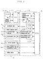
- Fig. 2 is a block diagram showing an electric structure of the image forming apparatus of Fig. 1.
- the image forming apparatus is an apparatus which overlaps toner images in four colors of yellow (Y), cyan (C), magenta (M) and black (K) to thereby form a full-color image or uses only a black (K) toner to thereby form a monochrome image.
- an engine controller 12 controls respective portions of an engine part E in accordance with an instruction from the main controller 11, whereby the image forming apparatus forms an image which corresponds to the image signal on a sheet S.
- the engine part E is capable of forming a toner image on a photosensitive member 21 of an image carrier unit 2. That is, the image carrier unit 2 comprises the photosensitive member 21 which is rotatable in the direction of an arrow in Fig. 1. Disposed around the photosensitive member 21 and in the rotation direction of the photosensitive member 21 in Fig. 1 are an electrifying roller 22 which serves as electrifying means, developers 23Y, 23C, 23M and 23K which serve as developing means, and a cleaning part 24. Applied with a high voltage from an electrifying bias generation part 121 and in contact with an outer peripheral surface of the photosensitive member 21, the electrifying roller 22 uniformly electrifies the outer peripheral surface of the photosensitive member 21.
- An exposure unit 3 irradiates laser light L toward the outer peripheral surface of the photosensitive member 21 which is electrified by the electrifying roller 22.
- the exposure unit 3, as shown in Fig. 2 is electrically connected with an image signal switching part 122.
- the laser light L scans over the photosensitive member 21 and consequently exposes the photosensitive member 21, whereby an electrostatic latent image corresponding to the image signal is formed on the photosensitive member 21.
- the image signal switching part 122 when the image signal switching part 122 is in conduction with a patch generation module 124, based on an instruction from a CPU 123 of the engine controller 12, a patch image signal outputted from the patch generation module 124 is fed to the exposure unit 3 so that a patch latent image is formed.
- the image signal switching part 122 when the image signal switching part 122 is in conduction with a CPU 111 of the main controller 11, the laser light L scans over and consequently exposes the photosensitive member 21 in accordance with an image signal which is supplied through an interface 112 from an external apparatus such as a host computer, so that an electrostatic latent image corresponding to the image signal is formed on the photosensitive member 21.
- the electrostatic latent image which is formed in this manner is developed by a developer part 23.
- disposed as the developer part 23 are the developer 23Y for yellow, the developer 23C for cyan, the developer 23M for magenta and the developer 23K for black which are arranged in this order around the photosensitive member 21.
- the developers 23Y, 23C, 23M and 23K are each structured so as to freely separate from and come close to the photosensitive member 21.
- one of the four developers 23Y, 23C, 23M and 23K selectively contacts the photosensitive member 21.
- a development bias generation part 125 thereafter applies a high voltage to the photosensitive member 21, and the toner in the selected color moves to the surface of the photosensitive member 21, thereby visualizing the electrostatic latent image on the photosensitive member 21.
- the voltages supplied to the respective developers may be simply D.C. voltages, or alternatively, A.C. voltages superimposed over D.C. voltages.
- the toner image developed by the developer part 23 is primarily transferred onto an intermediate transfer belt 41 of a transfer unit 4 in a primary transfer region R1 which is located between the black developer 23K and the cleaning part 24.
- a structure of the transfer unit 4 will be described in detail later.
- the cleaning part 24 is disposed at a position further ahead in a circumferential direction (the direction of the arrow in Fig. 1) from the primary transfer region R1, such that a toner remaining on the outer peripheral surface of the photosensitive member 21 after the primary transfer treatment is scraped off.
- the transfer unit 4 comprises rollers 42 through 47, the intermediate transfer belt 41 which is spun around the rollers 42 through 47, and a secondary transfer roller 48 which secondarily transfers an intermediate toner image transferred to the intermediate transfer belt 41 onto a sheet S.
- a transfer bias generation part 126 applies a primary transfer voltage upon the intermediate transfer belt 41. Toner images in the respective colors formed on the photosensitive member 21 are laid one atop the other on the intermediate transfer belt 41 into a color image, while the sheet S is taken out from a cassette 61, a hand-feeding tray 62 or an additional cassette (not shown) by a paper feed part 63 of a paper feed/discharge unit 6 and conveyed to a secondary transfer region R2.
- the color image is thereafter secondarily transferred onto the sheet S, thereby obtaining a full-color image.
- a monochrome image is to be transferred onto a sheet S
- only a black toner image on the photosensitive member 21 is formed on the intermediate transfer belt 41, and transferred onto a sheet conveyed to the secondary transfer region R2 to thereby obtain a monochrome image, as in the case of forming a color image.
- a toner remaining on and sticking to an outer peripheral surface of the intermediate transfer belt 41 is removed by a belt cleaner 49.
- the belt cleaner 49 is disposed opposite to the roller 46 across the intermediate transfer belt 41, and a cleaner blade contacts the intermediate transfer belt 41 at appropriate timing and scrapes off a toner from the outer peripheral surface of the intermediate transfer belt 41.
- a patch sensor PS which detects a density of a patch image which is formed on the outer peripheral surface of the intermediate transfer belt 41 as described later, and so is a read sensor for synchronization RS which detects a reference position of the intermediate transfer belt 41.
- the sheet S now seating the toner image transferred by the transfer unit 4 is conveyed by the paper feed part 63 of the paper feed/discharge unit 6 to a fixing unit 5 which is disposed on the downstream side to the secondary transfer region R2 along a predetermined paper feed path (dot-dot-dash line), and the toner image on the conveyed sheet S is fixed on the sheet S.
- the sheet S is thereafter conveyed to a paper discharge part 64 along the paper feed path 630.
- the paper discharge part 64 has two paper discharge paths 641a and 641b.
- the paper discharge path 641a extends from the fixing unit 5 to a standard paper discharge tray, while the paper discharge path 641b extends approximately parallel to the paper discharge path 641a between a paper re-feed part 66 and a multi-bin unit.
- Three roller pairs 642 through 644 are disposed along the paper discharge paths 641a and 641b, so as to discharge the sheets S toward the standard paper discharge tray or the multi-bin unit and convey the sheets S toward the paper re-feed part 66 for the purpose of forming images on non-printing surfaces of the sheets S.
- the paper re-feed part 66 is formed of three paper re-feed roller pairs 661 through 663 which are disposed along the paper re-feed path 664 as shown in Fig. 1.
- the sheet S sent from the paper discharge part 64 is returned to the gate roller pair 637 along the paper re-feed path 664 and a non-printing surface of the sheet S is directed toward the intermediate transfer belt 41 within the paper feed part 63, which makes it possible to secondarily transfer the image onto the non-printing surface.
- denoted at 113 is an image memory which is disposed in the main controller 11 such that the image memory stores image data supplied from an external apparatus such as a host computer through the interface 112, denoted at 127 is a RAM which temporarily stores control data for controlling the engine part E, a calculation result obtained by the CPU 123, etc., and denoted at 128 is a ROM which stores a calculation program which is executed by the CPU 123.
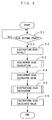
- Fig. 3 is a flow chart showing a density adjustment operation in the image forming apparatus of Fig. 1.
- the image forming apparatus may start setting the biases when the image forming apparatus becomes ready to form an image after a main power source of the image forming apparatus is turned on.
- the image forming apparatus may set the biases every few hours while a timer (not shown) disposed in the image forming apparatus measures hours of continuous use.
- steps S2 and S3 are executed to calculate an optimal development bias, and the calculated bias is set as the development bias (step S4).
- a step S5 is executed to calculate an optimal electrifying bias, and the calculated bias is set as the electrifying bias (step S6).
- the electrifying bias and the development bias are optimized in this manner. In the following, a detailed description will be given on an operation of each one of the development bias calculation (step S3) and the electrifying bias calculation (step S5).
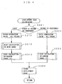
- Fig. 4 is a flow chart showing an operation of the development bias calculation shown in Fig. 3.
- the CPU 123 determines whether this is first calculation or the second or subsequent calculation after the main power source of the image forming apparatus is turned on (step S301).
- the current calculation is the first one, after setting up such that patch images will be created in all colors (which are the four colors of yellow (Y), cyan (C), magenta (M) and black (K) in this preferred embodiment) (step S311), an immediately subsequent step S312 is executed.
- a plurality of patch images are formed while gradually changing the development bias at relatively long intervals within a relatively wide range, thereby tentatively identifying a development bias which is necessary to obtain an optimal image density based on densities of the respective patch images.
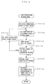
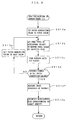
- Fig. 5 is a flow chart showing an operation of the bias calculation of Fig. 4 within a wide range.
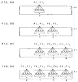
- Figs. 6A through 6D are schematic diagrams showing an operation of the processing of Fig. 5 and an operation of the bias calculation within narrow range which will be described later.
- a color in which patch images are to be generated is set as the first color, e.g., yellow (step S312a).
- the development bias is set to four different values which are apart at relatively long intervals (first intervals) within the wide range (step S312b).
- the wide range is the entirety of a programmable range (Vb01 - Vb10) of development bias which can be supplied to the developer part 23 from the development bias generation part 125, and four points Vb01, Vb04, Vb07 and Vb10 within the wide range (Vb01 - Vb10) are set as development biases.
- the first patch images PI1 are solid images in this preferred embodiment. The reason of this will be described in detail later.
- step S312d whether patch images are formed in all of patch generation colors is determined. While a result of the judgement stays NO, the next color is set as a patch generation color (step S312e) and the steps S312b and S312c are repeated. This adds further first patch images PI1 on the outer peripheral surface of the intermediate transfer belt 41, in the order of cyan (C), magenta (M) and black (K), as shown in Figs. 8B through 8D.
- C cyan
- M magenta
- K black
- a development bias corresponding to a target density is calculated at a step S312g, and the calculated bias is stored temporarily in the RAM 127 as an interim bias.
- a measurement result (image density) matches with the target density
- a development bias corresponding to this image density may be used as the interim bias.
- the two density values fail to match, as shown in Fig. 6B, it is possible to calculate an interim bias through linear interpolation, averaging or other appropriate methodology in accordance with data D (Vb04) and data D (Vb07) which are on the both sides of the target density.
- Fig. 9 is a flow chart showing an operation of the bias calculation (1) of Fig. 4 in the narrow range.
- a color in which patch images are to be generated is set as the first color, e.g., yellow (step S313a), as in the earlier calculation (step S312).
- the development bias is set to four different values which are apart at narrower intervals (second intervals) than the first intervals W1 within a narrow range which includes the interim bias (step S313b).
- the narrow range is approximately 1/3 of the programmable range (Vb01 - Vb10) of development bias.
- Vb01 - Vb10 the interim bias
- the interim bias is between development biases Vb05 and Vb06 as shown in Fig. 6B
- four points Vb04, Vb05, Vb06 and Vb07 are set as development biases (Fig. 6C).
- first patch images PI1 are sequentially formed on the photosensitive member 21 with this bias setup, and the solid images are transferred onto the outer peripheral surface of the intermediate transfer belt 41 as shown in Fig. 8A to thereby form first patch images PI1 (step S313c).
- step S312 the next color is set as a patch generation color (step S313e) and the steps S313b and S313c are repeated until it is determined at a step S313d that patch images are formed in all of patch generation colors.
- first patch images PI1 are further formed on the outer peripheral surface of the intermediate transfer belt 41, in the order of cyan (C), magenta (M) and black (K).
- step S313f image densities of the respective patch images PI1 are measured on the basis of a signal outputted from the patch sensor PS.
- step S313g a development bias corresponding to a target density is calculated.
- a measurement result image density
- a development bias corresponding to this image density may be used as an optimal development bias.
- the two density values fail to match, as shown in Fig. 6D, it is possible to calculate an optimal development bias through linear interpolation, averaging or other appropriate methodology in accordance with data D (Vb05) and data D (Vb06) which are on the both sides of the target density.
- the RAM 127 stores the optimal development bias which is calculated in this manner (step S302 in Fig. 4), and reads it out as the development bias during calculation of the electrifying bias which will be described later or while an image is formed in a normal manner.
- step S3 when the current calculation is determined to be the second or subsequent calculation after the main power source of the image forming apparatus is turned on, that is, when it is determined at the step S301 in Fig.
- step S321 an immediately subsequent step S322 is executed.
- bias calculation (2) within the narrow range is executed to thereby calculate an optimal development bias using biases which are measured immediately previously and stored in the RAM 127 as a reference.
- Fig. 10 is a flow chart showing an operation of the bias calculation (2) of Fig. 4 within the narrow range.
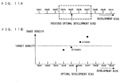
- Figs. 11A and 11B are schematic diagrams showing the operation of the processing shown in Fig. 10. This calculation processing is largely different from the bias calculation (1) within the narrow range described earlier in regard to the following.
- the electrifying bias set to the default value, and four different types of development biases are set based on an interim bias (step S313b).
- the electrifying bias is the optimal electrifying bias which is calculated through immediately preceding measurement and stored in the RAM 127, and four different types of development biases are set within the narrow range based on the optimal development bias which is stored in the RAM 127 (step S322b).
- the bias calculation (2) is structured otherwise the same as the bias calculation (1), and therefore, a redundant description will be simply omitted.
- the four different types of development biases are set.
- the four biases are apart at the second intervals within the narrow range using the development bias which is calculated immediately previously (preceding optimal development bias) without calculating an interim bias, the patch images are formed in the respective colors, and the optimal development bias is calculated.
- the first density adjustment step S312 + step S313
- the present invention realizes a unique effect that it is possible to calculate an optimal development bias at a high accuracy.
- the conventional technique three pairs of an electrifying bias and a development bias are stored in advance, and patch images are formed using the three development biases, respectively.
- patch images are formed using the three development biases, respectively.
- the development bias is changed within the narrow range including the immediately preceding optimal development bias out of the programmable range (Vb01 - Vb10) of development bias. That is, this preferred embodiment requires only approximately 1/3 of the programmable range of development bias, and the intervals of the development biases according to this preferred embodiment (second intervals) are narrower than those used in the conventional technique. Due to this, the present invention allows to calculate an optimal development bias at a better accuracy. It is to be noted that a simple reduction of the range in which a development bias is to be changed causes an optimal development bias to be calculated to deviate from the reduced range and only makes it difficult to accurately calculate an optimal development bias. However, according to this preferred embodiment, since the narrow range is set around an immediately preceding optimal development bias, it is extremely unlikely to see such a problem.
- the engine controller 12 writes the optimal development bias which is calculated in this manner over the preceding optimal development bias which is already stored in the RAM 127, thereby updating the optimal development bias (step S302 in Fig. 4).
- the sequence thereafter returns to Fig. 3 which requires to read the optimal development bias from the RAM 127 and set the retrieved optimal development bias as the development bias.
- An optimal electrifying bias is thereafter calculated (step S5) and set as the electrifying bias (step S6).
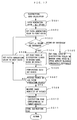
- Fig. 12 is a flow chart showing an operation of the electrifying bias calculation of Fig. 3.
- Figs. 13A and 13B are schematic diagrams showing the operation of the processing shown in Fig. 12.
- step S5 after setting up such that patch images will be created in all colors (which are the four colors of yellow (Y), cyan (C), magenta (M) and black (K) in this preferred embodiment) (step S501), a color in which second patch images are to be generated is set as the first color, e.g., yellow at a step S502.
- the CPU 123 determines whether the current electrifying bias calculation is first such calculation or the second or subsequent calculation after the main power source of the image forming apparatus is turned on (step S503). When the current calculation is determined to be the first one, a step S504 is executed. When the current calculation is determined to be the second or subsequent calculation, a step S505 is executed.
- the electrifying bias is set to four different values.
- the four biases are apart at relatively narrow intervals (third intervals) within the narrow range which includes the default value.
- the electrifying bias is set to four different values which are apart at relatively narrow intervals (third intervals) within the narrow range which includes a preceding optimal electrifying bias.
- the electrifying bias calculation executes only narrow-range calculation without calculating within the wide range.
- the narrow range is approximately 1/3 of a programmable range (Va01 - Va10) of electrifying bias.
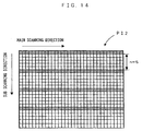
- respective yellow halftone images (See Fig. 14) are sequentially formed on the photosensitive member 21 and transferred onto the outer peripheral surface of the intermediate transfer belt 41, whereby second patch images PI2 are formed (Fig. 8A: step S506).
- the second patch images PI2 are halftone images in this preferred embodiment. The reason of this will be described in detail later, together with the reason that first patch images are solid images.
- step S507 whether the second patch images are formed in all of patch generation colors is judged. While a result of the judgement stays NO, the next color is set as a patch generation color (step S508) and the steps S503 through S507 are repeated. This adds further second patch images PI2 on the outer peripheral surface of the intermediate transfer belt 41, in the order of cyan (C), magenta (M) and black (K), as shown in Figs. 8B through 8D.
- C cyan
- M magenta
- K black
- an electrifying bias corresponding to a target density is calculated (step S510), and the calculated electrifying bias is stored in the RAM 127 as an optimal electrifying bias (step S511).
- an electrifying bias corresponding to this image density may be used as an optimal electrifying bias.
- it is possible to calculate an optimal electrifying bias through linear interpolation, averaging or other appropriate methodology in accordance with data D (Va05) and data D (Va06) which are on the both sides of the target density.
- the four types of electrifying biases are set up in the narrow range using biases which are measured immediately previously and stored in the RAM 127, the patch images are formed in the respective colors, and the optimal electrifying bias is calculated.
- this preferred embodiment realizes a similar effect to that of the development bias calculation.
- three pairs of an electrifying bias and a development bias are stored in advance, and patch images are formed using the three electrifying biases, respectively.
- the electrifying bias is changed within the narrow range including an immediately preceding optimal electrifying bias out of the programmable range (Va01 - Va10) of electrifying bias. That is, the preferred embodiment requires only approximately 1/3 of the programmable range of electrifying bias, and the intervals of the electrifying biases according to this preferred embodiment (third intervals W3) are narrower than those used in the conventional technique. Due to this, the present invention allows to calculate an optimal electrifying bias at a further higher accuracy. It is to be noted that a simple reduction of the range in which an electrifying bias is to be changed merely causes an optimal electrifying bias to be calculated to deviate from the reduced range and makes it difficult to accurately calculate an optimal electrifying bias. However, according to this preferred embodiment, since the narrow range is set around an immediately preceding optimal electrifying bias, it is extremely unlikely to see such a problem.
- the optimal electrifying bias calculated as described above is read from the RAM 127 and set as the electrifying bias, in addition to the optimal development bias already set as the development bias.
- the resultant image has the target density. In other words, the image density is stable.
- solid images are used as the first patch images for the development bias calculation while halftone images are used as the second patch images for the electrifying bias calculation in this preferred embodiment for the following reason.
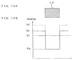
- an electrostatic latent image LI1 of a solid image (first patch image) PI1 (See Fig. 7) is formed on the surface of the photosensitive member 21 which is electrified uniformly at a surface potential V0, a surface potential corresponding to the electrostatic latent image LI1 largely drops down to a potential (exposed area potential) Von as shown in Figs. 15A and 15B, whereby a well potential is developed.
- the electrifying bias is increased to raise the surface potential of the photosensitive member 21 from the potential V0 up to a potential V0', the exposed area potential will not depart largely from the potential Von.
- a toner density is determined only in accordance with the development bias Vb despite any small change in the electrifying bias.
- a halftone image (second patch image) PI2 (See Fig. 14) contains line images formed at predetermined intervals.
- an electrostatic latent image LI2 of the halftone image is formed on the surface of the photosensitive member 21 which is electrified uniformly at a surface potential V0, surface potentials corresponding to the positions of the lines largely drop down to the potential (exposed area potential) Von, as shown in Figs. 16A and 16B.
- a comb-shaped well potential is developed. If the electrifying bias is increased in a similar manner to described above to raise the surface potential of the photosensitive member 21 from the potential V0 up to the potential V0', the exposed area potential corresponding to each line changes greatly from the potential Von to a potential Von'.
- the set development bias and the set electrifying bias strongly influence an eventual image.
- the preferred embodiment above requires to calculate an optimal development bias first. While changing the electrifying bias with the development bias set to the optimal development bias, the second patch images of halftone images are formed. As a result, therefore, the optimal electrifying bias needed to obtain an image density which meets the target density is calculated.
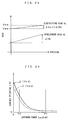
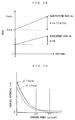
- Fig. 17 is a graph showing attenuation of a surface potential as a photosensitive member is exposed at various exposure powers, in which curves C(Va-1), C(Va-2), C(Va-3) and C(Va-4) express attenuation of a surface potential caused by electrification at electrifying biases Va-1 through Va-4 which are different from each other.
- "EXPOSURE POWER” denotes a dose of exposure applied upon a photosensitive member 21 per unit area from the exposure unit 3.
- a surface potential in a surface area of the exposed photosensitive member 21, namely, the exposed area potential changes in accordance with the electrifying bias and the exposure power supplied to the exposed photosensitive member 21 from the exposure unit 3.
- the exposed area potential is approximately the same between the attenuation curves regardless of a value of the electrifying bias when the exposure power is relatively large.
- the exposed area potential is different in accordance with the electrifying bias when the exposure power is relatively small. Such a tendency is as already described with reference to Figs. 15A, 15B, 16A and 16B.
- the electrifying bias is changed in accordance with a change in the development bias during the development bias calculation processing, to thereby solve the problem above which occurs when the exposure power is relatively small.
- a contrast potential Vcon1 changes in accordance with the change in the development bias Vb, thereby changing densities of the first patch images.
- the electrifying bias is set to various levels while fixing the development bias to the optimal development bias Vb, and latent images of second patch images are formed by exposing light at an exposure power P2.
- the exposed area potential of the latent images becomes largely different between the different electrifying bias levels.
- second patch images are halftone images as those shown in Fig. 16A.
- an effective exposure power for exposure with an isolated beam is smaller than the exposure power P1.
- the lowest potential level of a comb-shaped well potential is not as low as the lowest potential level which is observed during solid exposure.
- the exposed area potential becomes a potential Von2-2 to generate the contrast potential Vcon2-2 when the electrifying bias has the level Va-2
- the electrifying bias has the level Va-3
- the exposed area potential becomes a potential Von2-3 to generate the contrast potential Vcon2-3.
- the contrast potential Vcon2 changes as the electrifying bias Va changes, and a density of the second patch image accordingly changes.
- the electrifying bias calculation according to the preferred embodiment described above requires to form a plurality of second patch images while changing only the electrifying bias Va in order to determine an optimal electrifying bias.
- the optimal electrifying bias resulting from such electrifying bias calculation processing is different from the electrifying bias set during the development bias calculation (i.e., the electrifying bias Va-2 in Fig. 18), the contrast potential Vcon1 determined through the development bias calculation is changed.
- an image density may deviate from a target density. The possibility of this is high particularly when the exposure power drops.
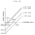
- Fig. 20 shows a relationship between the development bias Vb and the contrast potential which is identified based on the optimal attenuation curves C(Va-a) and C(Va-b).
- the horizontal axis denotes the development bias Vb while the vertical axis denotes the contrast potential.
- straight lines L(P1, Va-a), L(P1, Va-b), L(P2, Va-a) and L(P2, Va-b) respectively denote contrast potentials Vcon1-a, Vcon1-b, Vcon2-a and Vcon2-b which are shown in Fig. 21.
- a target contrast potential Vcon01 corresponds to the target density during the development bias calculation processing and a target contrast potential Vcon02 corresponds to the target density during the electrifying bias calculation processing.
- the development bias Vb is varied in its variable range while at the same time changing the electrifying bias from the level Va-a to the level Va-b.
- the electrifying biases Va-a and Va-b are set so that the two target contrast potentials Vcon01 and Vcon02 are simultaneously satisfied with approximately the same development bias Vb0, the optimal development bias Vb and the optimal electrifying bias Va are set at a high accuracy.
- Fig. 23 is a drawing showing a first variation of the development bias and the electrifying bias during the development bias calculation processing.
- Fig. 29 is a drawing showing a second variation of the development bias and the electrifying bias during the development bias calculation processing.
- Such setup is suitable to a situation where, as shown in Fig. 25, the exposure power P1 during the development bias calculation processing is relatively high thereby accompanying a small change in the exposed area potential Von1 with a change in the electrifying bias, whereas the exposure power P2 during the electrifying bias calculation processing is relatively low thereby accompanying a large change in the potential Von2 with a change in the electrifying bias. The reason of this will now be described with reference to Figs. 25 through 27.
- the straight line L(P2, Va-a) and the straight line L(P2, Va-b) shown in Fig. 26 are apart relatively far from each other. Because of this, even when the electrifying bias is changed from the level Va-a to the level Va-b, the contrast potential Vcon2 shows only a small change, thereby making it impossible sometimes to calculate appropriate values which are necessary to obtain the target contrast potential Vcon02.
- the second variation requires to set an electrifying bias change ⁇ Va smaller than a quantity of change ⁇ Vb in the development bias Vb.
- the straight line L(P2, Va-b) shifts closer to the straight line L(P2, Va-a) as shown in Fig. 27, accompanying a large change in the contrast potential Vcon2.
- Fig. 28 is a drawing showing a third variation of the development bias and the electrifying bias during the development bias calculation processing.
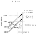
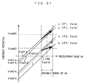
- Such setup is suitable to a situation where, as shown in Fig. 29, the exposure power P1 during the development bias calculation processing is relatively high thereby accompanying a small change in the exposed area potential Von1 with a change in the electrifying bias, and the exposure power P2 during the electrifying bias calculation processing is also relatively high thereby accompanying a small change in the potential Von2 with a change in the electrifying bias. The reason of this will now be described with reference to Figs. 29 through 31.
- the straight line L(P2, Va-a) and the straight line L(P2, Va-b) shown in Fig. 30 are apart relatively close to each other.
- the exposed area potentials Von2-a, Von2-b of second patch images shows only a small change, which arrives at virtually one optimal solution (the optimal electrifying bias).
- the target contrast potential Vcon01 of first patch images and the target contrast potential Vcon02 of second patch images sometimes become inconsistent to each other.
- a deviation ⁇ Vb0 is sometimes created between the optimal development bias Vb0 of first patch images and the optimal development bias of second patch images.
- the third variation requires to set the electrifying bias change ⁇ Va larger than a quantity of change ⁇ Vb in the development bias Vb (Fig. 28).
- the straight line L(P2, Va-b) is far from the straight line L(P2, Va-a) as shown in Fig. 31, thereby expanding a range of an optimal solution. This ensures consistency between the target contrast potential Vcon01 of first patch images and the target contrast potential Vcon02 of second patch images.
- the electrifying bias in accordance with a change in the development bias such that a development bias Vb01 satisfying the target contrast potential Vcon01 and a development bias Vb02 satisfying the target contrast potential Vcon02 become approximately equal to each other, as described above.
- a development bias Vb01 satisfying the target contrast potential Vcon01 and a development bias Vb02 satisfying the target contrast potential Vcon02 become approximately equal to each other, as described above.
- the development biases Vb01 and Vb02 it is difficult in some cases to match the development biases Vb01 and Vb02 with a linear change in the electrifying bias.
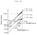
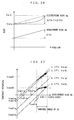
- the development bias Vb02 when the electrifying bias is changed according to the first variation (Fig. 23), the development bias Vb02 sometimes becomes smaller than the development bias Vb01 as shown in Fig. 32 to thereby create a deviation ⁇ Vb0 to the development bias.
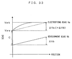
- the electrifying bias may be changed logarithmically as shown in Fig. 33, which moves the development bias Vb02 which satisfies the target contrast potential Vcon02 closer to the development bias Vb01 which satisfies the target contrast potential Vcon01 so that the two development biases Vb01 and Vb02 approximately match with each other (Fig. 34).
- the development bias Vb02 When the electrifying bias is changed according to the first variation (Fig. 23), the development bias Vb02 sometimes becomes larger than the development bias Vb01 as shown in Fig. 35, creating a deviation ⁇ Vb0 to the development bias.
- the electrifying bias may be changed exponentially as shown in Fig. 36, which moves the development bias Vb02 which satisfies the target contrast potential Vcon02 closer to the development bias Vb01 which satisfies the target contrast potential Vcon01 so that the two development biases Vb01 and Vb02 approximately match with each other (Fig. 37).
- the present invention is not limited to the preferred embodiment above, but can be modified in various manners other than those described above without departing from the essence of the present invention.
- the foregoing requires to use the electrifying roller 22 as the electrifying means, the present invention is applicable to an image forming apparatus in which non-contact electrifying means electrifies the photosensitive member 21.
- the preferred embodiment above is related to an image forming apparatus which is capable of forming a color image using toners in four colors
- an application of the present invention is not limited to this.
- the present invention is naturally applicable to an image forming apparatus which forms only a monochrome image as well.
- the image forming apparatus according to the preferred embodiment above is a printer for forming an image supplied from an external apparatus such as a host computer through the interface 112 on a sheet such as a copying paper, a transfer paper, a form and a transparent sheet for an over-head projector
- the present invention is applicable to image forming apparatuses of the electrophotographic method in general such as a copier machine and a facsimile machine.
- toner images on the photosensitive member 21 are transferred onto the intermediate transfer belt 41, image densities of patch images formed by said toner images are detected, and an optimal development bias and an optimal electrifying bias are thereafter calculated based on the detected image densities.
- the present invention is also applicable to an image forming apparatus in which a toner image is transferred onto other transfer medium except for the intermediate transfer belt 41, to thereby form a patch image.
- the other transfer medium includes a transfer drum, a transfer belt, a transfer sheet, an intermediate transfer drum, an intermediate transfer sheet, a reflection-type recording sheet, a transmission memory sheet, etc.
- a patch sensor may be disposed so as to detect a density of a patch image which is formed on a photosensitive member.
- the patch sensor detects image densities of patch images on the photosensitive member and an optimal development bias and an optimal electrifying bias are calculated based on the detected image densities.
- the RAM 127 of the engine controller 12 stores an optimal development bias and an optimal electrifying bias.
- the main power source of the image forming apparatus when the main power source of the image forming apparatus is turned off, the contents stored in the RAM 127 disappear.
- the image forming apparatus recognizes the current development bias calculation and the current electrifying bias calculation as "the first" calculation and executes processing in accordance with this recognition.
- a nonvolatile memory such as an EEPROM may be used to store an optimal development bias and an optimal electrifying bias which are calculated in sequence, so that as the main power source is turned on once again, the processing for "the second or subsequent" calculation is executed during the development bias calculation and the electrifying bias calculation.
- the narrow range is defines as approximately 1/3 of the programmable range (Vb01 - Vb10) of development bias in the preferred embodiment above.
- the width of the narrow range is not limited to this, if the width of the narrow range is wide, the use of the narrow range becomes less meaningful and degrades the accuracy of calculation of an optimal development bias. For this reason, it is necessary to set the narrow range as approximately 1/2 of or narrower than the programmable range for development bias. This also applies to the narrow range for electrifying biases as well.
- the number of bias values (the number of patch images) in the range is not limited to this but may be optional to the extent that more than one types of bias values are used.
- the number of bias values may be different between the wide range and the narrow range such that the number of patch images is different between the wide range and the narrow range.
- first patch images are each a solid image whose area ration is 100% in the preferred embodiment above, an image whose area ratio is approximately 80% or more may be used instead of using a solid image. Even when such an image is used as the first patch images, a similar effect to that promised when solid images are used is obtained.
- area ratio refers to a ratio of dots to the area of a patch image as a whole.
- the electrifying bias calculation (step S5) is further executed, in order to calculate an optimal development bias and an optimal electrifying bias.
- the manner in which an optimal development bias and an optimal electrifying bias are calculated is not limited to this.
- a plurality of patch images may be formed while changing the development bias and the electrifying bias at the same time, so that an optimal development bias and an optimal electrifying bias are calculated based on image densities of the patch images and density adjustment is executed.
- memory means such as a RAM and a ROM stores the development bias and the electrifying bias for every density adjustment and the memory means reads out the most recent development bias and the most recent electrifying bias in preparation for the next density adjustment.
- the plurality of patch images are formed while changing the development bias and the electrifying bias at the same time based on the most recent development bias and the most recent electrifying bias.
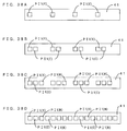
- the patch images PI1 are formed as clusters in each color as shown in Figs. 8A through 8D in the preferred embodiment described above, the patch images PI1 may be formed in each color in turn as shown in Figs. 38A through 38D. More specifically, first, yellow patch images PI1(Y) are formed on the intermediately transfer belt 41 at relatively wide intervals. Next, cyan patch images PI1(C) are formed one by one, starting at a position which is shifted by one patch image and a blank between the adjacent-patch images in the sub scanning direction (the right-hand side in Figs. 38A through 38D) as viewed from the yellow patch images PI1(Y).
- magenta patch images PI1(M) and black patch images PI1(K) are formed in a similar manner. Where the respective patch images are thus formed at relatively wide intervals, it is possible to ensure a stabilization time for switching of the biases, and hence, to form the respective patch images at the set biases without fail.
- first patch images the same directly applies to second patch images as well.
Landscapes
- Physics & Mathematics (AREA)
- General Physics & Mathematics (AREA)
- Engineering & Computer Science (AREA)
- Microelectronics & Electronic Packaging (AREA)
- Electrostatic Charge, Transfer And Separation In Electrography (AREA)
- Control Or Security For Electrophotography (AREA)
- Developing For Electrophotography (AREA)
- Color Electrophotography (AREA)
- Dry Development In Electrophotography (AREA)
- Display Devices Of Pinball Game Machines (AREA)
- Steering Control In Accordance With Driving Conditions (AREA)
- Transition And Organic Metals Composition Catalysts For Addition Polymerization (AREA)
Abstract
Description
Claims (16)
- An image forming apparatus for forming an image which has a predetermined target density, comprising: a photosensitive member (21); electrifying means (22) which electrifies a surface of said photosensitive member (21); exposing means (3) which forms an electrostatic latent image on the surface of said photosensitive member (21); developing means (23, 23Y, 23C, 23M, 23K) which visualizes said electrostatic latent image with a toner and forms a toner image; transferring means (4) which has a transfer medium (41) and transfers the toner image from said photosensitive member (21) to said transfer medium (41); density detecting means (PS) which detects an image density of the toner image on said photosensitive member (21) or on said transfer medium (41) as a patch image (PI1, PI2); control means (12) which controls an electrifying bias to be supplied to said electrifying means (22) and a development bias to be supplied to said development means (23, 23Y, 23C, 23M, 23K) based on a result of the detection obtained by said density detecting means (PS), and adjusts an image density of the toner image to a target density; and memory means (127) which stores the electrifying bias and the development bias, characterized in that:every time adjustment is finished, said control means (12) causes said memory means (127) to store the electrifying bias and the development bias which are obtained after the adjustment as an optimal electrifying bias and an optimal development bias, respectively; andwhen adjustment is performed repeatedly, based on said optimal electrifying bias and the optimal development bias stored in said memory means (127), said control means (12) controls such that a plurality of patch images (PI1, PI2) are formed in sequence while changing at least one of the electrifying bias and the development bias.
- The image forming apparatus according to claim 1, characterized in thatsaid control means (12) is capable of changing the development bias within a predetermined programmable range of development bias, andsaid control means (12) determines an optimal development bias which is needed to obtain the target density based on densities of first patch images (PI1) which are formed in the following bias condition: the electrifying bias is set to said optimal electrifying bias which is stored in said memory means (127); and the development bias is gradually changing within a range which is approximately 1/2 of or narrower than the programmable range of development bias and yet includes the most recent optimal development bias which is stored in said memory means (127).
- The image forming apparatus according to claim 2, characterized in that the area ratio of said first patch images (PI1) is 80% or more.
- The image forming apparatus according to claim 2 or 3, characterized in that said first patch images (PI1) are solid images.
- The image forming apparatus according to any of claims 2 through 4, characterized in thatsaid control means (12) is capable of changing the electrifying bias within a predetermined programmable range of electrifying bias, andsaid control means (12) determines an optimal electrifying bias which is needed to obtain the target density based on densities of second patch images (PI2) which are formed in the following bias condition: the development bias is set to the optimal development bias which is obtained based on densities of said first patch images (PI1); and the electrifying bias is gradually changing within a range which is approximately 1/2 of or narrower than the programmable range of electrifying bias and yet includes the most recent optimal electrifying bias which is stored in said memory means (127).
- The image forming apparatus according to claim 1, characterized in thatsaid control means (12) is capable of changing the electrifying bias within a predetermined programmable range of electrifying bias, andsaid control means (12) determines an optimal electrifying bias which is needed to obtain the target density based on densities of third patch images (PI2) which are formed in the following bias condition: the development bias is set to the optimal development bias which is stored in said memory means (127); and the electrifying bias is gradually changing within a range which is approximately 1/2 of or narrower than the programmable range of electrifying bias and yet includes the most recent optimal electrifying bias which is stored in said memory means (127).
- The image forming apparatus according to claim 5 or 6, wherein said third patch images (PI2) are halftone images.
- An image forming method in which after an electrifying bias is applied to electrifying means (22) to electrify a surface of a photosensitive member (21), an electrostatic latent image is formed on the surface of said photosensitive member (21), a development bias is applied to developing means (23,23Y,23C,23M,23K) so that said electrostatic latent image is visualized with a toner and a toner image is formed, characterized in that said method comprises the steps of:a first step in which after sequentially forming a plurality of toner images as patch images (PI1, PI2) while changing at least one of the electrifying bias and the development bias, densities of said patch images (PI1, PI2) are detected, and an optimal development bias and an optimal electrifying bias which are needed to obtain a target density are determined based on image densities of said patch images (PI1, PI2); anda second step of storing the optimal development bias and said optimal electrifying bias in memory means (127), whereinwhen said first step is to be repeated again after executing said second step, based on the most recent optimal development bias and the most recent optimal electrifying bias which are stored in said memory means (127), a plurality of patch images (PI1, PI2) are formed in sequence while changing at least one of the electrifying bias and the development bias.
- The image forming method according to claim 8, characterized in that said first step comprises:a first sub step in which the electrifying bias is fixed at the most recent optimal electrifying bias which is stored in said memory means (127), and after sequentially forming a plurality of first patch images (PI1) while changing the development bias based on the most recent optimal development bias which is stored in said memory means (127), densities of said first patch images (PI1) are detected, and an optimal development bias which is needed to obtain a target density is determined based on the image densities of said first patch images (PI1).
- The image forming method according to claim 9, characterized in that used as said first patch images (PI1) at said first sub step are images whose the area ratio is 80% or more.
- The image forming method according to claim 9 or 10, wherein said first patch images (PI1) are solid images.
- The image forming method according to any of claims 9 through 11, characterized in that said first step further comprises: a second sub step in which the development bias is fixed at the optimal development bias which is determined at said first sub step, and after sequentially forming a plurality of second patch images (PI2) while changing the electrifying bias based on the most recent optimal electrifying bias which is stored in said memory means (127), densities of said second patch images (PI2) are detected, and an optimal electrifying bias which is needed to obtain the target density is determined based on the image densities of said second patch images (PI2).
- The image forming method according to claim 8, characterized in that said first step further comprises: a third sub step in which the development bias is fixed at the optimal development bias which is stored in said memory means (127), and after sequentially forming a plurality of second patch images (PI2) while changing the electrifying bias based on the most recent optimal electrifying bias which is stored in said memory means (127), densities of said second patch images (PI2) are detected, and an optimal electrifying bias which is needed to obtain the target density is determined based on the image densities of said second patch images (PI2).
- The image forming method according to claim 12 or 13, wherein halftone images are formed as said second patch images (PI2) at said third sub step.
- The image forming method according to any of claims 8 through 14, characterized in that said patch images (PI1, PI2) are toner images which are formed on the surface of said photosensitive member.
- The image forming method according to any of claims 8 through 14, characterized in that said patch images (PI1, PI2) are toner images which are obtained by transferring said toner images formed on the surface of said photosensitive member onto a transfer medium.
Applications Claiming Priority (2)
| Application Number | Priority Date | Filing Date | Title |
|---|---|---|---|
| JP21365599A JP3199062B2 (en) | 1999-07-28 | 1999-07-28 | Image forming apparatus and image forming method |
| JP21365599 | 1999-07-28 |
Publications (3)
| Publication Number | Publication Date |
|---|---|
| EP1074892A2 true EP1074892A2 (en) | 2001-02-07 |
| EP1074892A3 EP1074892A3 (en) | 2002-04-17 |
| EP1074892B1 EP1074892B1 (en) | 2004-12-29 |
Family
ID=16642770
Family Applications (1)
| Application Number | Title | Priority Date | Filing Date |
|---|---|---|---|
| EP00306132A Expired - Lifetime EP1074892B1 (en) | 1999-07-28 | 2000-07-19 | Image forming apparatus and method |
Country Status (5)
| Country | Link |
|---|---|
| US (1) | US6483997B1 (en) |
| EP (1) | EP1074892B1 (en) |
| JP (1) | JP3199062B2 (en) |
| AT (1) | ATE286269T1 (en) |
| DE (1) | DE60017026T2 (en) |
Cited By (1)
| Publication number | Priority date | Publication date | Assignee | Title |
|---|---|---|---|---|
| US6917772B2 (en) | 2001-07-23 | 2005-07-12 | Canon Kabushiki Kaisha | Image forming apparatus for controlling density of image, detachably attachable device, and memory device |
Families Citing this family (15)
| Publication number | Priority date | Publication date | Assignee | Title |
|---|---|---|---|---|
| US6553191B1 (en) * | 2000-09-11 | 2003-04-22 | Toshiba Tec Kabushiki Kaisha | Adjustment-control system for image forming apparatus |
| KR100472474B1 (en) * | 2002-08-30 | 2005-03-10 | 삼성전자주식회사 | Method for reducing consumption of developer of electrophotographic processor and electrophotographic processor using the same |
| EP1623281A2 (en) * | 2003-03-27 | 2006-02-08 | Eastman Kodak Company | Method and system for wide format toning |
| JP4301366B2 (en) * | 2003-11-27 | 2009-07-22 | 株式会社リコー | Image forming system |
| JP5288241B2 (en) * | 2008-02-07 | 2013-09-11 | 株式会社リコー | Image forming apparatus and image density control method |
| JP5267916B2 (en) * | 2008-06-30 | 2013-08-21 | 株式会社リコー | Image forming apparatus and image density control method |
| US9046850B2 (en) | 2011-02-04 | 2015-06-02 | Ricoh Company, Ltd. | Image forming apparatus capable of reducing image density irregularity |
| US8526835B2 (en) * | 2011-04-19 | 2013-09-03 | Xerox Corporation | Closed loop controls for transfer control in first transfer for optimized image content |
| JP2013113989A (en) * | 2011-11-28 | 2013-06-10 | Brother Ind Ltd | Image forming apparatus and method for correcting image formation |
| JP2013250532A (en) | 2012-06-04 | 2013-12-12 | Canon Inc | Image forming apparatus |
| JP6024512B2 (en) * | 2013-02-26 | 2016-11-16 | 富士ゼロックス株式会社 | Image forming apparatus |
| JP6187218B2 (en) * | 2013-12-11 | 2017-08-30 | コニカミノルタ株式会社 | Image forming apparatus and voltage setting method |
| JP6260271B2 (en) * | 2013-12-27 | 2018-01-17 | ブラザー工業株式会社 | Image forming apparatus |
| JP7073779B2 (en) * | 2018-02-22 | 2022-05-24 | コニカミノルタ株式会社 | Image forming device and development condition correction method |
| JP7643217B2 (en) * | 2021-07-07 | 2025-03-11 | 沖電気工業株式会社 | Image forming device |
Family Cites Families (21)
| Publication number | Priority date | Publication date | Assignee | Title |
|---|---|---|---|---|
| JP2532073B2 (en) | 1986-12-05 | 1996-09-11 | 株式会社リコー | Residual potential correction method |
| JPH0313441A (en) | 1989-06-12 | 1991-01-22 | Mita Ind Co Ltd | Picture image forming device |
| US5298944A (en) * | 1989-06-30 | 1994-03-29 | Ricoh Company, Ltd. | Testing image density to control toner concentration and dynamic range in a digital copier |
| US5124750A (en) * | 1989-09-05 | 1992-06-23 | Minolta Camera Kabushiki Kaisha | Toner density detecting method, and image forming method and apparatus employing the toner density detecting method |
| JPH03236751A (en) | 1990-02-13 | 1991-10-22 | Satake Eng Co Ltd | Packaging of polished rice and packed polished rice |
| JPH03260667A (en) * | 1990-03-12 | 1991-11-20 | Minolta Camera Co Ltd | Image forming device |
| JP3124540B2 (en) | 1990-08-10 | 2001-01-15 | 株式会社リコー | Image forming device |
| JPH0430182A (en) * | 1990-05-28 | 1992-02-03 | Ricoh Co Ltd | Electrophotographic image forming device |
| JP3013441B2 (en) * | 1990-11-30 | 2000-02-28 | ミノルタ株式会社 | Digital image forming equipment |
| US5453773A (en) | 1990-11-30 | 1995-09-26 | Minolta Camera Kabushiki Kaisha | Electrophotographic image forming apparatus comprising means for automatically adjusting image reproduction density |
| JPH0540397A (en) | 1991-08-06 | 1993-02-19 | Fuji Xerox Co Ltd | Automatic adjusting method for high-voltage power source output for corotron |
| JPH05333648A (en) | 1992-06-01 | 1993-12-17 | Sharp Corp | Process control method |
| JPH06102735A (en) * | 1992-09-24 | 1994-04-15 | Toshiba Corp | Image forming device |
| JP3236751B2 (en) * | 1995-02-02 | 2001-12-10 | 株式会社日立製作所 | Image forming device |
| JP3460432B2 (en) | 1996-03-13 | 2003-10-27 | ミノルタ株式会社 | Image forming device |
| JPH1055081A (en) | 1996-08-08 | 1998-02-24 | Fuji Xerox Co Ltd | Image forming device |
| JP3584142B2 (en) | 1997-02-28 | 2004-11-04 | キヤノン株式会社 | Image forming device |
| JP3503732B2 (en) | 1997-06-27 | 2004-03-08 | 富士ゼロックス株式会社 | Image forming device |
| JP3260667B2 (en) | 1997-09-04 | 2002-02-25 | 有限会社エヌ・エー | Skin current heating device |
| JPH11133682A (en) | 1997-11-04 | 1999-05-21 | Matsushita Electric Ind Co Ltd | Electrophotographic copying machine |
| US6243542B1 (en) * | 1998-12-14 | 2001-06-05 | Canon Kabushiki Kaisha | System for controlling the density of toner images in an image forming apparatus |
-
1999
- 1999-07-28 JP JP21365599A patent/JP3199062B2/en not_active Expired - Fee Related
-
2000
- 2000-07-19 DE DE60017026T patent/DE60017026T2/en not_active Expired - Lifetime
- 2000-07-19 AT AT00306132T patent/ATE286269T1/en not_active IP Right Cessation
- 2000-07-19 EP EP00306132A patent/EP1074892B1/en not_active Expired - Lifetime
- 2000-07-24 US US09/625,056 patent/US6483997B1/en not_active Expired - Fee Related
Cited By (1)
| Publication number | Priority date | Publication date | Assignee | Title |
|---|---|---|---|---|
| US6917772B2 (en) | 2001-07-23 | 2005-07-12 | Canon Kabushiki Kaisha | Image forming apparatus for controlling density of image, detachably attachable device, and memory device |
Also Published As
| Publication number | Publication date |
|---|---|
| DE60017026T2 (en) | 2005-06-09 |
| US6483997B1 (en) | 2002-11-19 |
| EP1074892A3 (en) | 2002-04-17 |
| EP1074892B1 (en) | 2004-12-29 |
| JP3199062B2 (en) | 2001-08-13 |
| JP2001042580A (en) | 2001-02-16 |
| ATE286269T1 (en) | 2005-01-15 |
| DE60017026D1 (en) | 2005-02-03 |
Similar Documents
| Publication | Publication Date | Title |
|---|---|---|
| EP1074894B1 (en) | Image forming apparatus and method | |
| EP1074892B1 (en) | Image forming apparatus and method | |
| EP1074891B1 (en) | Image forming apparatus and method | |
| JP2008216776A (en) | Image forming apparatus, controller and program | |
| JP5288241B2 (en) | Image forming apparatus and image density control method | |
| JP3186747B2 (en) | Image forming apparatus and image forming method | |
| JP3250549B2 (en) | Image forming apparatus and image forming method | |
| JP3843701B2 (en) | Image forming apparatus and image forming method | |
| JP2002099119A (en) | Image forming apparatus and image forming method | |
| JP3674614B2 (en) | Image forming apparatus and image forming method | |
| JP3767328B2 (en) | Image forming apparatus and image forming method | |
| JP3446750B2 (en) | Image forming apparatus and image forming method | |
| JP3729023B2 (en) | Image forming apparatus and image forming method | |
| JP2005326890A (en) | Image forming apparatus and image forming method | |
| JP2006106222A (en) | Image forming apparatus and its developing bias value setting method | |
| JP2002091100A (en) | Image forming apparatus and image forming method | |
| JP2002091094A (en) | Image forming apparatus and image forming method | |
| JP3446727B2 (en) | Image forming apparatus and image forming method | |
| JP3550650B2 (en) | Image forming method and image forming apparatus | |
| US20200142339A1 (en) | Image forming apparatus, and method and program for controlling image forming apparatus | |
| JP3591706B2 (en) | Image forming method and image forming apparatus | |
| JP2001075318A (en) | Density adjusting method and density adjusting device in image forming apparatus | |
| JP2003015372A (en) | Image forming apparatus and image forming method | |
| JP2003177637A (en) | Image forming apparatus and image forming method | |
| JP2003223023A (en) | Image forming apparatus and image forming method |
Legal Events
| Date | Code | Title | Description |
|---|---|---|---|
| PUAI | Public reference made under article 153(3) epc to a published international application that has entered the european phase |
Free format text: ORIGINAL CODE: 0009012 |
|
| AK | Designated contracting states |
Kind code of ref document: A2 Designated state(s): AT BE CH CY DE DK ES FI FR GB GR IE IT LI LU MC NL PT SE |
|
| AX | Request for extension of the european patent |
Free format text: AL;LT;LV;MK;RO;SI |
|
| PUAL | Search report despatched |
Free format text: ORIGINAL CODE: 0009013 |
|
| AK | Designated contracting states |
Kind code of ref document: A3 Designated state(s): AT BE CH CY DE DK ES FI FR GB GR IE IT LI LU MC NL PT SE |
|
| AX | Request for extension of the european patent |
Free format text: AL;LT;LV;MK;RO;SI |
|
| RIC1 | Information provided on ipc code assigned before grant |
Free format text: 7G 03G 15/00 A, 7G 03G 15/06 B, 7G 03G 15/02 B |
|
| 17P | Request for examination filed |
Effective date: 20020701 |
|
| AKX | Designation fees paid |
Free format text: AT BE CH CY DE DK ES FI FR GB GR IE IT LI LU MC NL PT SE |
|
| 17Q | First examination report despatched |
Effective date: 20031204 |
|
| GRAP | Despatch of communication of intention to grant a patent |
Free format text: ORIGINAL CODE: EPIDOSNIGR1 |
|
| GRAS | Grant fee paid |
Free format text: ORIGINAL CODE: EPIDOSNIGR3 |
|
| GRAA | (expected) grant |
Free format text: ORIGINAL CODE: 0009210 |
|
| AK | Designated contracting states |
Kind code of ref document: B1 Designated state(s): AT BE CH CY DE DK ES FI FR GB GR IE IT LI LU MC NL PT SE |
|
| PG25 | Lapsed in a contracting state [announced via postgrant information from national office to epo] |
Ref country code: IT Free format text: LAPSE BECAUSE OF FAILURE TO SUBMIT A TRANSLATION OF THE DESCRIPTION OR TO PAY THE FEE WITHIN THE PRESCRIBED TIME-LIMIT;WARNING: LAPSES OF ITALIAN PATENTS WITH EFFECTIVE DATE BEFORE 2007 MAY HAVE OCCURRED AT ANY TIME BEFORE 2007. THE CORRECT EFFECTIVE DATE MAY BE DIFFERENT FROM THE ONE RECORDED. Effective date: 20041229 Ref country code: AT Free format text: LAPSE BECAUSE OF FAILURE TO SUBMIT A TRANSLATION OF THE DESCRIPTION OR TO PAY THE FEE WITHIN THE PRESCRIBED TIME-LIMIT Effective date: 20041229 Ref country code: NL Free format text: LAPSE BECAUSE OF FAILURE TO SUBMIT A TRANSLATION OF THE DESCRIPTION OR TO PAY THE FEE WITHIN THE PRESCRIBED TIME-LIMIT Effective date: 20041229 Ref country code: CH Free format text: LAPSE BECAUSE OF FAILURE TO SUBMIT A TRANSLATION OF THE DESCRIPTION OR TO PAY THE FEE WITHIN THE PRESCRIBED TIME-LIMIT Effective date: 20041229 Ref country code: BE Free format text: LAPSE BECAUSE OF FAILURE TO SUBMIT A TRANSLATION OF THE DESCRIPTION OR TO PAY THE FEE WITHIN THE PRESCRIBED TIME-LIMIT Effective date: 20041229 Ref country code: FI Free format text: LAPSE BECAUSE OF FAILURE TO SUBMIT A TRANSLATION OF THE DESCRIPTION OR TO PAY THE FEE WITHIN THE PRESCRIBED TIME-LIMIT Effective date: 20041229 Ref country code: LI Free format text: LAPSE BECAUSE OF FAILURE TO SUBMIT A TRANSLATION OF THE DESCRIPTION OR TO PAY THE FEE WITHIN THE PRESCRIBED TIME-LIMIT Effective date: 20041229 |
|
| REG | Reference to a national code |
Ref country code: GB Ref legal event code: FG4D |
|
| REG | Reference to a national code |
Ref country code: CH Ref legal event code: EP |
|
| REG | Reference to a national code |
Ref country code: IE Ref legal event code: FG4D |
|
| REF | Corresponds to: |
Ref document number: 60017026 Country of ref document: DE Date of ref document: 20050203 Kind code of ref document: P |
|
| PG25 | Lapsed in a contracting state [announced via postgrant information from national office to epo] |
Ref country code: DK Free format text: LAPSE BECAUSE OF FAILURE TO SUBMIT A TRANSLATION OF THE DESCRIPTION OR TO PAY THE FEE WITHIN THE PRESCRIBED TIME-LIMIT Effective date: 20050329 Ref country code: SE Free format text: LAPSE BECAUSE OF FAILURE TO SUBMIT A TRANSLATION OF THE DESCRIPTION OR TO PAY THE FEE WITHIN THE PRESCRIBED TIME-LIMIT Effective date: 20050329 Ref country code: GR Free format text: LAPSE BECAUSE OF FAILURE TO SUBMIT A TRANSLATION OF THE DESCRIPTION OR TO PAY THE FEE WITHIN THE PRESCRIBED TIME-LIMIT Effective date: 20050329 |
|
| PG25 | Lapsed in a contracting state [announced via postgrant information from national office to epo] |
Ref country code: ES Free format text: LAPSE BECAUSE OF FAILURE TO SUBMIT A TRANSLATION OF THE DESCRIPTION OR TO PAY THE FEE WITHIN THE PRESCRIBED TIME-LIMIT Effective date: 20050409 |
|
| NLV1 | Nl: lapsed or annulled due to failure to fulfill the requirements of art. 29p and 29m of the patents act | ||
| REG | Reference to a national code |
Ref country code: CH Ref legal event code: PL |
|
| PG25 | Lapsed in a contracting state [announced via postgrant information from national office to epo] |
Ref country code: CY Free format text: LAPSE BECAUSE OF FAILURE TO SUBMIT A TRANSLATION OF THE DESCRIPTION OR TO PAY THE FEE WITHIN THE PRESCRIBED TIME-LIMIT Effective date: 20050719 Ref country code: LU Free format text: LAPSE BECAUSE OF NON-PAYMENT OF DUE FEES Effective date: 20050719 Ref country code: IE Free format text: LAPSE BECAUSE OF NON-PAYMENT OF DUE FEES Effective date: 20050719 |
|
| PG25 | Lapsed in a contracting state [announced via postgrant information from national office to epo] |
Ref country code: MC Free format text: LAPSE BECAUSE OF NON-PAYMENT OF DUE FEES Effective date: 20050731 |
|
| ET | Fr: translation filed | ||
| PLBE | No opposition filed within time limit |
Free format text: ORIGINAL CODE: 0009261 |
|
| STAA | Information on the status of an ep patent application or granted ep patent |
Free format text: STATUS: NO OPPOSITION FILED WITHIN TIME LIMIT |
|
| 26N | No opposition filed |
Effective date: 20050930 |
|
| REG | Reference to a national code |
Ref country code: IE Ref legal event code: MM4A |
|
| PG25 | Lapsed in a contracting state [announced via postgrant information from national office to epo] |
Ref country code: PT Free format text: LAPSE BECAUSE OF NON-PAYMENT OF DUE FEES Effective date: 20050529 |
|
| PGFP | Annual fee paid to national office [announced via postgrant information from national office to epo] |
Ref country code: FR Payment date: 20100805 Year of fee payment: 11 Ref country code: DE Payment date: 20100714 Year of fee payment: 11 |
|
| PGFP | Annual fee paid to national office [announced via postgrant information from national office to epo] |
Ref country code: GB Payment date: 20100714 Year of fee payment: 11 |
|
| GBPC | Gb: european patent ceased through non-payment of renewal fee |
Effective date: 20110719 |
|
| REG | Reference to a national code |
Ref country code: FR Ref legal event code: ST Effective date: 20120330 |
|
| PG25 | Lapsed in a contracting state [announced via postgrant information from national office to epo] |
Ref country code: DE Free format text: LAPSE BECAUSE OF NON-PAYMENT OF DUE FEES Effective date: 20120201 Ref country code: FR Free format text: LAPSE BECAUSE OF NON-PAYMENT OF DUE FEES Effective date: 20110801 |
|
| REG | Reference to a national code |
Ref country code: DE Ref legal event code: R119 Ref document number: 60017026 Country of ref document: DE Effective date: 20120201 |
|
| PG25 | Lapsed in a contracting state [announced via postgrant information from national office to epo] |
Ref country code: GB Free format text: LAPSE BECAUSE OF NON-PAYMENT OF DUE FEES Effective date: 20110719 |