EP1073877B1 - Endpoint detection in chemical mechanical polishing (cmp) by substrate holder elevation detection - Google Patents
Endpoint detection in chemical mechanical polishing (cmp) by substrate holder elevation detection Download PDFInfo
- Publication number
- EP1073877B1 EP1073877B1 EP99920030A EP99920030A EP1073877B1 EP 1073877 B1 EP1073877 B1 EP 1073877B1 EP 99920030 A EP99920030 A EP 99920030A EP 99920030 A EP99920030 A EP 99920030A EP 1073877 B1 EP1073877 B1 EP 1073877B1
- Authority
- EP
- European Patent Office
- Prior art keywords
- substrate holder
- substrate
- planarizing
- backside
- elevation
- Prior art date
- Legal status (The legal status is an assumption and is not a legal conclusion. Google has not performed a legal analysis and makes no representation as to the accuracy of the status listed.)
- Expired - Lifetime
Links
Images


Classifications
-
- H—ELECTRICITY
- H01—ELECTRIC ELEMENTS
- H01L—SEMICONDUCTOR DEVICES NOT COVERED BY CLASS H10
- H01L21/00—Processes or apparatus adapted for the manufacture or treatment of semiconductor or solid state devices or of parts thereof
- H01L21/02—Manufacture or treatment of semiconductor devices or of parts thereof
- H01L21/04—Manufacture or treatment of semiconductor devices or of parts thereof the devices having at least one potential-jump barrier or surface barrier, e.g. PN junction, depletion layer or carrier concentration layer
- H01L21/18—Manufacture or treatment of semiconductor devices or of parts thereof the devices having at least one potential-jump barrier or surface barrier, e.g. PN junction, depletion layer or carrier concentration layer the devices having semiconductor bodies comprising elements of Group IV of the Periodic System or AIIIBV compounds with or without impurities, e.g. doping materials
- H01L21/30—Treatment of semiconductor bodies using processes or apparatus not provided for in groups H01L21/20 - H01L21/26
- H01L21/302—Treatment of semiconductor bodies using processes or apparatus not provided for in groups H01L21/20 - H01L21/26 to change their surface-physical characteristics or shape, e.g. etching, polishing, cutting
- H01L21/304—Mechanical treatment, e.g. grinding, polishing, cutting
-
- B—PERFORMING OPERATIONS; TRANSPORTING
- B24—GRINDING; POLISHING
- B24B—MACHINES, DEVICES, OR PROCESSES FOR GRINDING OR POLISHING; DRESSING OR CONDITIONING OF ABRADING SURFACES; FEEDING OF GRINDING, POLISHING, OR LAPPING AGENTS
- B24B37/00—Lapping machines or devices; Accessories
- B24B37/005—Control means for lapping machines or devices
- B24B37/013—Devices or means for detecting lapping completion
-
- B—PERFORMING OPERATIONS; TRANSPORTING
- B24—GRINDING; POLISHING
- B24B—MACHINES, DEVICES, OR PROCESSES FOR GRINDING OR POLISHING; DRESSING OR CONDITIONING OF ABRADING SURFACES; FEEDING OF GRINDING, POLISHING, OR LAPPING AGENTS
- B24B49/00—Measuring or gauging equipment for controlling the feed movement of the grinding tool or work; Arrangements of indicating or measuring equipment, e.g. for indicating the start of the grinding operation
- B24B49/12—Measuring or gauging equipment for controlling the feed movement of the grinding tool or work; Arrangements of indicating or measuring equipment, e.g. for indicating the start of the grinding operation involving optical means
-
- G—PHYSICS
- G01—MEASURING; TESTING
- G01B—MEASURING LENGTH, THICKNESS OR SIMILAR LINEAR DIMENSIONS; MEASURING ANGLES; MEASURING AREAS; MEASURING IRREGULARITIES OF SURFACES OR CONTOURS
- G01B11/00—Measuring arrangements characterised by the use of optical techniques
- G01B11/02—Measuring arrangements characterised by the use of optical techniques for measuring length, width or thickness
- G01B11/026—Measuring arrangements characterised by the use of optical techniques for measuring length, width or thickness by measuring distance between sensor and object
-
- G—PHYSICS
- G01—MEASURING; TESTING
- G01B—MEASURING LENGTH, THICKNESS OR SIMILAR LINEAR DIMENSIONS; MEASURING ANGLES; MEASURING AREAS; MEASURING IRREGULARITIES OF SURFACES OR CONTOURS
- G01B11/00—Measuring arrangements characterised by the use of optical techniques
- G01B11/02—Measuring arrangements characterised by the use of optical techniques for measuring length, width or thickness
- G01B11/06—Measuring arrangements characterised by the use of optical techniques for measuring length, width or thickness for measuring thickness ; e.g. of sheet material
- G01B11/0608—Height gauges
-
- G—PHYSICS
- G01—MEASURING; TESTING
- G01B—MEASURING LENGTH, THICKNESS OR SIMILAR LINEAR DIMENSIONS; MEASURING ANGLES; MEASURING AREAS; MEASURING IRREGULARITIES OF SURFACES OR CONTOURS
- G01B11/00—Measuring arrangements characterised by the use of optical techniques
- G01B11/02—Measuring arrangements characterised by the use of optical techniques for measuring length, width or thickness
- G01B11/06—Measuring arrangements characterised by the use of optical techniques for measuring length, width or thickness for measuring thickness ; e.g. of sheet material
- G01B11/0616—Measuring arrangements characterised by the use of optical techniques for measuring length, width or thickness for measuring thickness ; e.g. of sheet material of coating
- G01B11/0683—Measuring arrangements characterised by the use of optical techniques for measuring length, width or thickness for measuring thickness ; e.g. of sheet material of coating measurement during deposition or removal of the layer
-
- H—ELECTRICITY
- H01—ELECTRIC ELEMENTS
- H01L—SEMICONDUCTOR DEVICES NOT COVERED BY CLASS H10
- H01L21/00—Processes or apparatus adapted for the manufacture or treatment of semiconductor or solid state devices or of parts thereof
- H01L21/02—Manufacture or treatment of semiconductor devices or of parts thereof
- H01L21/04—Manufacture or treatment of semiconductor devices or of parts thereof the devices having at least one potential-jump barrier or surface barrier, e.g. PN junction, depletion layer or carrier concentration layer
- H01L21/18—Manufacture or treatment of semiconductor devices or of parts thereof the devices having at least one potential-jump barrier or surface barrier, e.g. PN junction, depletion layer or carrier concentration layer the devices having semiconductor bodies comprising elements of Group IV of the Periodic System or AIIIBV compounds with or without impurities, e.g. doping materials
- H01L21/30—Treatment of semiconductor bodies using processes or apparatus not provided for in groups H01L21/20 - H01L21/26
- H01L21/302—Treatment of semiconductor bodies using processes or apparatus not provided for in groups H01L21/20 - H01L21/26 to change their surface-physical characteristics or shape, e.g. etching, polishing, cutting
- H01L21/306—Chemical or electrical treatment, e.g. electrolytic etching
- H01L21/30625—With simultaneous mechanical treatment, e.g. mechanico-chemical polishing
-
- H—ELECTRICITY
- H01—ELECTRIC ELEMENTS
- H01L—SEMICONDUCTOR DEVICES NOT COVERED BY CLASS H10
- H01L22/00—Testing or measuring during manufacture or treatment; Reliability measurements, i.e. testing of parts without further processing to modify the parts as such; Structural arrangements therefor
- H01L22/20—Sequence of activities consisting of a plurality of measurements, corrections, marking or sorting steps
- H01L22/26—Acting in response to an ongoing measurement without interruption of processing, e.g. endpoint detection, in-situ thickness measurement
Definitions
- the present invention relates to a method of monitoring performance of a planarization process in the manufacturing of microelectronic devices. Moreover, the invention relates to a planarization machine. Specifically, the invention is related to a method of planarization of a microelectronic substrate.
- CMP Chemical-mechanical polishing or mechanical polishing processes
- a microelectronic substrate e.g ., a semiconductor wafer
- a planarizing medium e.g ., a polishing pad
- a planarizing fluid e.g ., an abrasive slurry
- the planarizing fluid may contain small, abrasive particles to abrade the surface of the wafer, but a non-abrasive planarizing fluid may be used with fixed-abrasive polishing pads.
- the planarizing fluid has chemicals that etch and/or oxidize the surface of the wafer.
- the polishing pad is generally a planar pad made from a porous material, such as blown polyurethane, and it may also have abrasive particles bonded to the material.
- material is removed from the surface of the wafer by the abrasive particles (mechanical removal) and the chemicals (chemical removal).
- FIG 1 schematically illustrates a conventional CMP machine 10 with a platen 20, a wafer carrier 30, a polishing pad 40, and a slurry 44 on the polishing pad.
- the platen 20 has a surface 22 upon which the polishing pad 40 is positioned.
- a drive assembly 26 rotates the platen 20 as indicated by arrow "A”.
- the drive assembly 26 reciprocates the platen back and forth as indicated by arrow "B". The motion of the platen 20 is imparted to the pad 40 because the polishing pad 40 frictionally engages the surface 22 of the platen 20.
- the wafer carrier 30 has a lower surface 32 to which a wafer 60 may be attached, or the wafer 60 may be attached to a resilient pad 34 positioned between the wafer 60 and the lower surface 32.
- the wafer carrier 30 may be a weighted, free-floating wafer carrier, or an actuator assembly 36 may be attached to the wafer carrier 30 to impart axial and rotational motion, as indicated by arrows "C" and "D", respectively.
- the wafer 60 is positioned face-downward against the polishing pad 40, and then the platen 20 and the wafer carrier 30 move relative to one another. As the face of the wafer 60 moves across the planarizing surface 42 of the polishing pad 40, the polishing pad 40 and the slurry 44 remove material from the wafer 60.
- the throughput of CMP processes is a function of several factors. one of which is the ability to accurately stop the CMP process at a desired endpoint. Accurately stopping the CMP process at a desired endpoint is important to maintaining a high throughput because the thickness of the dielectric layer must be within an acceptable range; if the thickness of the dielectric layer is not within an acceptable range. the wafer must be re-polished until it reaches the desired endpoint. Re-polishing a wafer, however, significantly reduces the throughput of CMP processes. Thus, it is highly desirable to stop the CMP process at the desired endpoint.
- the polishing period of one wafer in a run is estimated using the polishing rate of previous wafers in the run.
- the estimated polishing period for the wafer may not be accurate because the polishing rate may change from one wafer to another. Thus, this method may not accurately polish the wafer to the desired endpoint.
- the wafer is removed from the pad and wafer carrier, and then the thickness of the wafer is measured. Removing the wafer from the pad and wafer carrier, however. is time-consuming and may damage the wafer. Moreover, if the wafer is not at the desired endpoint. then even more time is required to re-mount the wafer to the wafer carrier for repolishing. Thus, this method generally reduces the throughput of the CMP process.
- a portion of the wafer is moved beyond the edge of the pad, and an interferometer directs a beam of light directly onto the exposed portion of the wafer.
- the wafer may not be in the same reference position each time it overhangs the pad because the edge of the pad is compressible, the wafer may pivot when it overhangs the pad, and the exposed portion of the wafer may vary from one measurement to the next. Thus, this method may inaccurately measure the change in thickness of the wafer.
- CMP processes In addition to accurately determining the endpoint of CMP processes. it is also desirable to monitor other performance characteristics or parameters to maintain the throughput and quality of finished wafers.
- the performance of CMP processes may be affected by the pad condition, the distribution of planarizing fluid under the wafer, and many other planarizing parameters. Monitoring these parameters, however, is difficult because it is time consuming to interrupt processing wafers to determine whether one of the parameters has changed. Moreover, if the CMP process is stopped and all of the parameters appear to be in an acceptable range, it is a complete waste of processing time. Thus, it would also be desirable to monitor the performance of CMP processing to ensure that the planarizing parameters are within acceptable operating ranges without interrupting the process.
- US-A-5 667 424 discloses a method of monitoring performance of planarization of a microelectronic substrate. To this end, the back side of a substrate holder is measured. This prior art method makes use of vibrations enduced within the substrate holder.
- US-A-5 777 739 discloses to measure a change of a distance with means of an interferrometer.
- the invention is defined in claims 1, 20 and 26. Preferred embodiment are defined by the dependent claims 2 - 19 and 21 - 25.
- An endpoint detector measures the change in thickness of a semiconductor wafer while the wafer is attached to a wafer carrier during chemical-mechanical polishing of the wafer.
- the endpoint detector has a reference platform, a measuring face, and a distance measuring device.
- the reference platform is positioned proximate to the wafer carrier, and the reference platform and measuring device are positioned apart from one another by a known, constant distance for all of the measurements of a single wafer.
- the measuring face is fixedly positioned with respect to the wafer carrier at a location that allows the measuring device to engage the measuring face when the wafer is positioned on the reference platform. Each time the measuring device engages the measuring surface, it measures the displacement of the measuring face with respect to the measuring device. The displacement of the measuring face is proportional to the change in thickness of the wafer between measurements.
- the wafer is placed on the reference platform before it is polished, and then the measuring device engages the measuring surface to determine a baseline measurement of the position of the measuring face with respect to the measuring device. After the wafer is at least partially polished, the wafer is re-placed on the reference platform and the measuring device is re-engaged with the measuring face to determine a subsequent measurement of the position of the measuring face with respect to the measuring device. The displacement of the measuring face from the baseline measurement to the subsequent measurement is proportionate to the change in thickness of the wafer.
- a planarizing machine includes a flat plate, a planarizing medium fastened to the plate, a carrier assembly to manipulate a substrate with respect to the planarizing medium, and a non-contact distance measuring device.
- the carrier assembly more specifically, may have a support structure and a substrate holder coupled to the support structure.
- the substrate holder typically has a mounting site facing the planarizing medium to carry the substrate, and a backside facing away from the planarizing medium.
- the non-contact distance measuring device may also be attached to the support structure to be positioned over the substrate holder for at least a portion of the planarizing process. Additionally, the support structure typically holds the non-contact measuring device at a known elevation with respect to the plate to measure an actual distance between the backside of the substrate holder and the known elevation while the substrate is planarized.
- the distance measuring device may have a beam emitter that projects a source beam, a reflector positioned at a predetermined angle with respect to the plate to direct the source beam against the backside of the substrate holder, and a primary detector to receive a return beam reflected from the backside of the substrate holder normal to the source beam.
- the primary detector monitors a lateral shift of the return beam and provides a signal to a processor that determines the distance between the backside of the substrate holder and the intersection between the source beam and the return beam.
- the distance measuring device may measure a first actual distance at one stage of the planarization process and then re-measure a second actual distance at a subsequent stage of the planarization process to determine the change in thickness of the substrate, the polishing rate of the substrate and several other performance parameters of the planarization process while the substrate is planarized.
- the present invention is directed toward performance monitoring systems, such as an endpoint detector that quickly and accurately measures a change in wafer thickness of a semiconductor wafer or another type of microelectronic substrate during chemical-mechanical polishing of the wafer.
- One aspect of the invention is to provide a reference platform upon which the wafer is positioned each time a measurement is taken.
- Another aspect of the invention is to provide a measuring face on the wafer carrier that may be engaged by a measuring device without removing the wafer from either the reference platform or the wafer carrier. As will be discussed in greater detail below, by providing such a reference platform and a measuring face, the change in wafer thickness can be quickly and accurately measured while the wafer is attached to the wafer carrier and positioned on the reference platform.
- certain embodiments of performance monitoring systems may also determine the actual elevation of the wafer carrier with respect to a known elevation to monitor the endpoint, the polishing rate, and several other performance parameters of CMP processes.
- Many specific details of certain embodiments of the invention are set forth in Figures 2-7 to provide a thorough understanding of such embodiments.
- One skilled in the art, however, will understand that the present invention may have additional embodiments and may be practiced without several of the details described in the following detailed description of the invention.
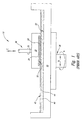
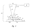
- Figure 2 illustrates an endpoint detector 50 used in a conventional CMP machine in which a wafer 60 or another type of microelectronic substrate is mounted in a substrate holder or wafer carrier 30.
- the wafer carrier 30 is typically attached to an actuator 36 that manipulates the wafer carrier 30.
- the endpoint detector 50 includes a reference platform 70, a measuring face 80 on the wafer carrier 30, and a measuring device 90.
- An upper surface 72 on the reference platform 70 is maintained at a fixed distance from the measuring device 90 over all of the measurements of a single wafer.
- the measuring face 80 is positioned on an upper face 38 of the wafer carrier 30 so that it is exposed to the measuring device 90 when the wafer carrier 30 presses the wafer 60 against the reference surface 70.
- the measuring face 80 is preferably a planar, reflective surface that is either the upper surface 38 of the wafer carrier itself, or a separate panel attached to the wafer carrier 80.
- the measuring device 90 engages the measuring face 80 to measure the displacement of the measuring face 80 with respect to the fixed position of the measuring device 90.
- the measuring device is an interferometer with an emitter 92 and a receiver 94.
- the emitter directs a beam of light onto the measuring face 80. which reflects the light beam back to the receiver 94.
- a controller 96 connected to the receiver 94 translates the phase change of the reflected light beam into a measurement of the vertical displacement of the measuring face 80 with respect to the position of the measuring device 90.
- both the reference platform 70 and the measuring device 90 are fixed against displacement with respect to each other to maintain a constant distance therebetween over all of the measurements of a single wafer.
- the distance between the reference platform 70 and the measuring device 90 may change from one wafer to another.
- the endpoint detector 50 therefore, eliminates one variable of many conventional endpoint techniques that commonly produces inaccurate measurements of the change in thickness of the wafer 60.
- the wafer carrier 30 initially places the wafer 60 on the upper surface 72 of the reference platform 70 before the wafer 60 is polished.
- the measuring face 80 is positioned at a height h 1 with respect to the measuring device 90.
- the emitter 92 then directs the light beam 93 onto the measuring face 80 to determine a baseline measurement of the position of the measuring face 80 at the height h 1 .
- the wafer is polished for a period of time.
- the change in thickness of the wafer ( ⁇ t) is equal to the distance between an original surface 62 of the wafer and a new surface 62(a).
- the wafer 60 is then re-placed on the upper surface 72 of the reference platform 70, and the position of the measuring face 80 accordingly changes to a height h 2 .
- the light beam 93 from the measuring device 90 re-engages the measuring face 80 to measure the displacement ( ⁇ d) of the measuring face 80 at the height h 2 .
- the displacement ⁇ d of the measuring face 80 is proportional to, and may directly correspond to, the change in thickness ⁇ t of the wafer 60.
- One advantage of the endpoint detector 50 is that it provides highly accurate measurements of the change in thickness ⁇ t of the wafer 60.
- An aspect of the invention is that the distance is constant between the upper surface 72 of the reference platform 70 and the measuring device 90 over all of the measurements of a single wafer. Accordingly, the displacement ⁇ d of the measuring surface 80 is caused by the change in thickness ⁇ t of the wafer 60. Moreover, by measuring the displacement of the measuring face 80, the wafer 60 does not need to overhang the reference platform 70 as in conventional techniques that directly impinge the wafer with a light beam. The endpoint detector 50, therefore, provides highly accurate measurements of the change in thickness ⁇ t of the wafer 60.
- FIG 3 schematically illustrates a polishing machine 52 with an endpoint detector in accordance with the invention.
- the reference platform 70 is the polishing pad 40.
- the upper surface 72 of the platform 70 is accordingly the upper surface of the polishing pad 40.
- the wafer carrier 30 places the wafer 60 on the polishing pad/reference platform 70 to polish the wafer 60 and to measure the change in thickness of the wafer 60.
- the measuring device 90 engages the measuring face 80.
- the change in thickness of the wafer is measured as described above with respect to Figure 2.
- This embodiment of the invention is particularly useful for rigid pads or semi-rigid pads that compress substantially less than the change in thickness of the wafer.
- polishing pad/reference platform 70 is compressible, the measurements made by the endpoint detector of the polishing machine 52 will be accurate as long as any force exerted on the pad/platform 70 is the same for all measurements.
- the polishing machine 52 quickly measures the change in thickness of the wafer 60 because the wafer 60 is not removed from either the wafer carrier 30 or the polishing pad/reference platform 70. Therefore, this particular embodiment of the invention enhances the throughput compared to conventional CMP processes.
- Figures 4-6 illustrate several embodiments of polishing machines with endpoint detectors.
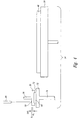
- Figure 4 shows a polishing machine 54 with an endpoint detector in which the reference platform 70 is a separate pedestal 74 that is fixed to the ground or the planarization machine.
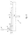
- Figure 5 shows a polishing machine 56 with an endpoint detector in which the reference platform 70 is spaced radially outwardly away from the polishing pad 40 on the surface of the platen 20.
- a reference platform 70(a) may be positioned in a hole 43 at the center of the pad 40, or the hole 43 can provide access to a reference platform 70(b) defined by the center of the upper surface 22 of the platen 20.
- Figure 6 shows a polishing machine 58 with an endpoint detector in which the reference platform 70 is attached to a wall 14 of the polishing machine.
- the change in thickness of the wafer 60 is measured by moving the wafer 60 from the polishing pad 40 to the reference platform 70.
- the change in displacement of the measuring face 80 is measured by engaging the measuring face 80 with a light beam from the measuring device 90, as described above with respect to Figure 2.
- polishing machines 52, 54, 56, and 58 are generally enhance the throughput of the CMP process.
- the change in thickness ⁇ t of the wafer 60 may be measured without removing the wafer 60 from the wafer carrier 30 or the polishing pad. Accordingly, the change in thickness ⁇ t of the wafer 60 may be measured in situ with only minimal interruption of the polishing of the wafer 60.
- the change in thickness ⁇ t of the wafer 60 may be measured without removing the wafer 60 from the wafer carrier 30. Thus, the change in thickness ⁇ t of the wafer may be measured with only a minor interruption to move the wafer between the polishing pad and the reference platform.
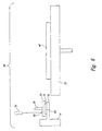
- FIG 7 is a schematic cross-sectional view of a CMP machine 110 in accordance with another embodiment of the invention.
- the CMP machine 110 may have a housing 112, a cavity 114 in the housing 112, and a barrier 116 in the cavity 114.
- An actuator 126 attached to the housing 112 has a shaft 127 within the barrier 116 to support a plate or platen 120. The actuator 126 may accordingly rotate the plate 120 via the shaft 127.
- the planarizing machine 110 also has a carrier assembly 130 attached to the housing 112.
- the carrier assembly 130 has a primary actuator 131 that moves a first arm 132 vertically along a sweep axis P-P (arrow V) and rotates the arm 132 along the sweep axis P-P (arrow R 1 ).
- the arm 132 may carry a secondary actuator 134 with a drive shaft 135 coupled to a substrate holder or wafer carrier 136.
- the substrate holder 136 preferably has a backside or upper face 138, a plurality of nozzles 139 for dispensing a planarizing fluid 144, and a mounting site to which a microelectronic substrate 12 may be attached.
- the substrate 12 for example, may be a semiconductor wafer or a field emission display with or without integrated circuitry.
- the carrier assembly 130 manipulates the substrate holder 136 to engage and translate the substrate 12 across a planarizing surface 142 of a planarizing medium 140 ( e . g ., a polishing pad).
- the carrier assembly 130 may also have a second arm 133 that rotates about the sweep axis P-P (arrow R 2 ).
- the first and second arms 132 and 133 are preferably independently operable from another.
- the first arm 132 may be coupled to the primary actuator 131 to be moved with respect to the sweep axis P-P as set forth above.
- the second arm 133 may have a vertical portion that telescopes from the vertical portion of the first arm 132.
- the second arm 133 may be independently coupled to a secondary actuator 131a on the planarizing machine 110.
- the secondary actuator 131a may accordingly move the second arm 133 about the sweep axis P-P at a fixed or known elevation as the first arm 132 independently moves with respect to the sweep axis P-P.
- the second arm 133 may rotate about the sweep axis P-P with the first arm 132 at a constant elevation.
- the planarizing machine 110 may also have a performance monitoring system 190 attached to the second arm 133.
- the performance monitoring system 190 may be a non-contact distance measuring device 191 ("distance device") with a beam emitter 192, a reflector 193 spaced apart from the beam emitter 192, and a detector 194.
- the beam emitter 192 projects a beam 195 (indicated in Figure 7 by reference numbers 195a-c) to determine the actual elevation of the substrate holder 136. As schematically shown in Figure 7, the beam emitter 192 may project an initial portion of a source beam 195a toward the reflector 193.
- the reflector 193 is inclined at an angle ⁇ that directs an intermediate portion of the source beam 195b to the backside 138 of the substrate holder 136 so that a detector 194 receives a return beam 195c.
- the detector 194 receives the return beam 195c and optically detects the lateral position "L" of the return beam 195c with respect to a scale (not shown) in the detector 194.
- a processor 198 operatively coupled to the distance device 191 determines the actual distance "d" between the backside 138 of the substrate holder 136 and the initial portion of the source beam 195a. Accordingly, the distance device 191 measures the actual elevation of the backside 138 of the substrate holder 136.
- the distance device 191 is preferably a triangular displacement meter that accurately measures the distance between the known elevation and the backside 138 of the substrate holder 136.
- the beam emitter 192 may accordingly be a laser, and the beam 195 may accordingly be a laser beam.
- One suitable laser displacement meter is the LC3 displacement meter manufactured by Keyence Corporation of Woodcliff Lake. New Jersey.
- the distance device 191 directs the beam 195 against the backside 138 of the substrate holder 136 as the carrier assembly 130 presses the substrate 12 against the planarizing medium 140.
- the distance measuring device 191 directs the beam 195 against the backside 138 of the substrate holder 136 while the substrate holder 136 and the planarizing medium 140 are stationary.
- the distance measuring device 191 directs the beam 195 against the substrate holder 136 while imparting relative motion between the substrate holder 136 and the planarizing medium 140.
- the distance device 191 and the substrate holder 136 may rotate together about the sweep axis P-P during the planarization process so that the beam 195 continuously impinges the backside 138 of the substrate holder 136.
- the distance device 191 may be positioned at a fixed point along the planarizing path of the substrate holder 136 so that the beam 195 periodically impinges the backside 138 of the substrate holder 136 during the planarization process. In either case, the distance device 191 detects the elevation of the backside of the substrate holder 136 with respect to the known elevation by measuring a first actual distance at one stage of the planarization process and by re-measuring a second actual distance at a subsequent stage. As explained in more detail below, the distance between the known elevation and the backside 138 of the substrate holder 136 provides data to monitor the performance of the planarization process.
- the performance monitoring system 190 of the planarizing machine 110 may detect the endpoint of the planarization process.
- the distance device 191 measures the elevation of the backside 138 of the substrate holder 136.
- the planarizing machine 110 terminates the removal of material from the substrate 12.
- the planarizing machine 110 may terminate the process by disengaging the substrate 12 from the planarizing medium 140 or stopping the relative motion between the substrate 12 and the planarizing medium 140.
- the performance monitoring system 190 may also monitor other system parameters to indicate when the planarization process is not operating at a desired level.
- the processor 198 may determine the polishing rate of the substrate 12 without interrupting the planarizing cycle by correlating the change in elevation of the substrate holder 136 with the elapsed time of the cycle.
- a significant change in the polishing rate generally indicates that one of the planarizing parameters is not operating within a desired range.
- a drop in the polishing rate for example. may indicate that the condition of the polishing pad has deteriorated such that the pad does not uniformly remove material from the substrate.
- a significant change in the polishing rate may also indicate that another polishing parameter is not within a desired operating range. Therefore, the planarizing machine 110 may also monitor other system parameters to indicate whether the planarization process is operating within a desired range.
- the performance monitoring systems 190 may measure the vertical motion of the substrate holder to determine whether anomalies occur in the vertical displacement pattern of the substrate holder.
- the substrate holder 136 is attached to the shaft 137 by a gimbal joint. Accordingly, even though the substrate holder 136 should desirably remain level during planarization, most substrate holders have a pattern of small vertical displacement under normal operating conditions.
- the distance device 191 can also measure and indicate the vertical displacement pattern of the substrate holder 136 during planarization. Accordingly, if the vertical displacement pattern changes or large anomalies occur, it may indicate that the pad surface, the slurry distribution or the substrate surface is not within a normal operating range. Therefore, the planarizing machine 110 also provides another source of information for monitoring the planarizing characteristics of the planarization process.
Landscapes
- Engineering & Computer Science (AREA)
- General Physics & Mathematics (AREA)
- Physics & Mathematics (AREA)
- Microelectronics & Electronic Packaging (AREA)
- Power Engineering (AREA)
- Manufacturing & Machinery (AREA)
- Computer Hardware Design (AREA)
- Mechanical Engineering (AREA)
- Condensed Matter Physics & Semiconductors (AREA)
- Mechanical Treatment Of Semiconductor (AREA)
- Length Measuring Devices By Optical Means (AREA)
- Finish Polishing, Edge Sharpening, And Grinding By Specific Grinding Devices (AREA)
- Constituent Portions Of Griding Lathes, Driving, Sensing And Control (AREA)
Abstract
Description
- The present invention relates to a method of monitoring performance of a planarization process in the manufacturing of microelectronic devices. Moreover, the invention relates to a planarization machine. Specifically, the invention is related to a method of planarization of a microelectronic substrate.
- Chemical-mechanical polishing or mechanical polishing processes (collectively "CMP") remove material from the surface of a microelectronic substrate (e.g., a semiconductor wafer) in the production of ultra-high density integrated circuits. In a typical CMP process, a wafer is pressed against a planarizing medium (e.g., a polishing pad) in the presence of a planarizing fluid (e.g., an abrasive slurry) under controlled chemical, pressure, velocity, and temperature conditions. The planarizing fluid may contain small, abrasive particles to abrade the surface of the wafer, but a non-abrasive planarizing fluid may be used with fixed-abrasive polishing pads. Additionally, the planarizing fluid has chemicals that etch and/or oxidize the surface of the wafer. The polishing pad is generally a planar pad made from a porous material, such as blown polyurethane, and it may also have abrasive particles bonded to the material. Thus, when the pad and/or the wafer moves with respect to the other, material is removed from the surface of the wafer by the abrasive particles (mechanical removal) and the chemicals (chemical removal).
- Figure 1 schematically illustrates a
conventional CMP machine 10 with aplaten 20, awafer carrier 30, apolishing pad 40, and aslurry 44 on the polishing pad. Theplaten 20 has asurface 22 upon which thepolishing pad 40 is positioned. Adrive assembly 26 rotates theplaten 20 as indicated by arrow "A". In another type of existing CMP machine, thedrive assembly 26 reciprocates the platen back and forth as indicated by arrow "B". The motion of theplaten 20 is imparted to thepad 40 because thepolishing pad 40 frictionally engages thesurface 22 of theplaten 20. Thewafer carrier 30 has alower surface 32 to which awafer 60 may be attached, or thewafer 60 may be attached to aresilient pad 34 positioned between thewafer 60 and thelower surface 32. Thewafer carrier 30 may be a weighted, free-floating wafer carrier, or anactuator assembly 36 may be attached to thewafer carrier 30 to impart axial and rotational motion, as indicated by arrows "C" and "D", respectively. - In the operation of the
conventional polisher 10, thewafer 60 is positioned face-downward against thepolishing pad 40, and then theplaten 20 and thewafer carrier 30 move relative to one another. As the face of thewafer 60 moves across the planarizingsurface 42 of thepolishing pad 40, thepolishing pad 40 and theslurry 44 remove material from thewafer 60. - In the competitive semiconductor industry, it is highly desirable to maximize the throughput of CMP processes to produce accurate, planar surfaces as quickly as possible. The throughput of CMP processes is a function of several factors. one of which is the ability to accurately stop the CMP process at a desired endpoint. Accurately stopping the CMP process at a desired endpoint is important to maintaining a high throughput because the thickness of the dielectric layer must be within an acceptable range; if the thickness of the dielectric layer is not within an acceptable range. the wafer must be re-polished until it reaches the desired endpoint. Re-polishing a wafer, however, significantly reduces the throughput of CMP processes. Thus, it is highly desirable to stop the CMP process at the desired endpoint.
- In one conventional method for determining the endpoint of the CMP process, the polishing period of one wafer in a run is estimated using the polishing rate of previous wafers in the run. The estimated polishing period for the wafer, however, may not be accurate because the polishing rate may change from one wafer to another. Thus, this method may not accurately polish the wafer to the desired endpoint.
- In another method for determining the endpoint of the CMP process, the wafer is removed from the pad and wafer carrier, and then the thickness of the wafer is measured. Removing the wafer from the pad and wafer carrier, however. is time-consuming and may damage the wafer. Moreover, if the wafer is not at the desired endpoint. then even more time is required to re-mount the wafer to the wafer carrier for repolishing. Thus, this method generally reduces the throughput of the CMP process.
- In still another method for determining the endpoint of the CMP process, a portion of the wafer is moved beyond the edge of the pad, and an interferometer directs a beam of light directly onto the exposed portion of the wafer. The wafer, however, may not be in the same reference position each time it overhangs the pad because the edge of the pad is compressible, the wafer may pivot when it overhangs the pad, and the exposed portion of the wafer may vary from one measurement to the next. Thus, this method may inaccurately measure the change in thickness of the wafer.
- In light of the problems with conventional endpoint detection techniques, it would be desirable to develop an apparatus and a method for quickly and accurately measuring the change in thickness of a wafer during the CMP process.
- In addition to accurately determining the endpoint of CMP processes. it is also desirable to monitor other performance characteristics or parameters to maintain the throughput and quality of finished wafers. The performance of CMP processes may be affected by the pad condition, the distribution of planarizing fluid under the wafer, and many other planarizing parameters. Monitoring these parameters, however, is difficult because it is time consuming to interrupt processing wafers to determine whether one of the parameters has changed. Moreover, if the CMP process is stopped and all of the parameters appear to be in an acceptable range, it is a complete waste of processing time. Thus, it would also be desirable to monitor the performance of CMP processing to ensure that the planarizing parameters are within acceptable operating ranges without interrupting the process.
- US-A-5 667 424 discloses a method of monitoring performance of planarization of a microelectronic substrate. To this end, the back side of a substrate holder is measured. This prior art method makes use of vibrations enduced within the substrate holder.
- US-A-5 777 739 discloses to measure a change of a distance with means of an interferrometer.
- The invention is defined in
claims - The wafer is placed on the reference platform before it is polished, and then the measuring device engages the measuring surface to determine a baseline measurement of the position of the measuring face with respect to the measuring device. After the wafer is at least partially polished, the wafer is re-placed on the reference platform and the measuring device is re-engaged with the measuring face to determine a subsequent measurement of the position of the measuring face with respect to the measuring device. The displacement of the measuring face from the baseline measurement to the subsequent measurement is proportionate to the change in thickness of the wafer.
- A planarizing machine includes a flat plate, a planarizing medium fastened to the plate, a carrier assembly to manipulate a substrate with respect to the planarizing medium, and a non-contact distance measuring device. The carrier assembly, more specifically, may have a support structure and a substrate holder coupled to the support structure. The substrate holder typically has a mounting site facing the planarizing medium to carry the substrate, and a backside facing away from the planarizing medium. The non-contact distance measuring device may also be attached to the support structure to be positioned over the substrate holder for at least a portion of the planarizing process. Additionally, the support structure typically holds the non-contact measuring device at a known elevation with respect to the plate to measure an actual distance between the backside of the substrate holder and the known elevation while the substrate is planarized.
- The distance measuring device may have a beam emitter that projects a source beam, a reflector positioned at a predetermined angle with respect to the plate to direct the source beam against the backside of the substrate holder, and a primary detector to receive a return beam reflected from the backside of the substrate holder normal to the source beam. The primary detector monitors a lateral shift of the return beam and provides a signal to a processor that determines the distance between the backside of the substrate holder and the intersection between the source beam and the return beam. Accordingly, the distance measuring device may measure a first actual distance at one stage of the planarization process and then re-measure a second actual distance at a subsequent stage of the planarization process to determine the change in thickness of the substrate, the polishing rate of the substrate and several other performance parameters of the planarization process while the substrate is planarized.
-
- Figure 1 is a schematic cross-sectional view of a conventional chemical-mechanical polishing machine in accordance with the prior art.
- Figure 2 is a schematic cross-sectional view of an endpoint detector in accordance with the invention.
- Figure 3 is a schematic cross-sectional view of a polisher with an endpoint detector in accordance with the invention.
- Figure 4 is a schematic cross-sectional view of a polisher with an endpoint detector in accordance with the invention.
- Figure 5 is a schematic cross-sectional view of a polisher with an endpoint detector in accordance with the invention.
- Figure 6 is a schematic cross-sectional view of a polisher with an endpoint detector in accordance with the invention.
- Figure 7 is a schematic cross-sectional view of another polishing machine with a performance monitoring system in accordance with another embodiment of the invention.
-
- The present invention is directed toward performance monitoring systems, such as an endpoint detector that quickly and accurately measures a change in wafer thickness of a semiconductor wafer or another type of microelectronic substrate during chemical-mechanical polishing of the wafer. One aspect of the invention is to provide a reference platform upon which the wafer is positioned each time a measurement is taken. Another aspect of the invention is to provide a measuring face on the wafer carrier that may be engaged by a measuring device without removing the wafer from either the reference platform or the wafer carrier. As will be discussed in greater detail below, by providing such a reference platform and a measuring face, the change in wafer thickness can be quickly and accurately measured while the wafer is attached to the wafer carrier and positioned on the reference platform. In addition to measuring the change in wafer thickness, certain embodiments of performance monitoring systems according to the invention may also determine the actual elevation of the wafer carrier with respect to a known elevation to monitor the endpoint, the polishing rate, and several other performance parameters of CMP processes. Many specific details of certain embodiments of the invention are set forth in Figures 2-7 to provide a thorough understanding of such embodiments. One skilled in the art, however, will understand that the present invention may have additional embodiments and may be practiced without several of the details described in the following detailed description of the invention.
- Figure 2 illustrates an
endpoint detector 50 used in a conventional CMP machine in which awafer 60 or another type of microelectronic substrate is mounted in a substrate holder orwafer carrier 30. Thewafer carrier 30 is typically attached to anactuator 36 that manipulates thewafer carrier 30. Theendpoint detector 50 includes areference platform 70, a measuringface 80 on thewafer carrier 30, and a measuringdevice 90. Anupper surface 72 on thereference platform 70 is maintained at a fixed distance from the measuringdevice 90 over all of the measurements of a single wafer. The measuringface 80 is positioned on anupper face 38 of thewafer carrier 30 so that it is exposed to the measuringdevice 90 when thewafer carrier 30 presses thewafer 60 against thereference surface 70. The measuringface 80 is preferably a planar, reflective surface that is either theupper surface 38 of the wafer carrier itself, or a separate panel attached to thewafer carrier 80. The measuringdevice 90 engages the measuringface 80 to measure the displacement of the measuringface 80 with respect to the fixed position of the measuringdevice 90. - In one embodiment, the measuring device is an interferometer with an
emitter 92 and areceiver 94. The emitter directs a beam of light onto the measuringface 80. which reflects the light beam back to thereceiver 94. As the distance between the measuringface 80 and the measuringdevice 90 changes in correspondence to the change in thickness of thewafer 60, the phase of the reflected light beam at thereceiver 94 changes accordingly. Acontroller 96 connected to thereceiver 94 translates the phase change of the reflected light beam into a measurement of the vertical displacement of the measuringface 80 with respect to the position of the measuringdevice 90. Importantly, both thereference platform 70 and the measuringdevice 90 are fixed against displacement with respect to each other to maintain a constant distance therebetween over all of the measurements of a single wafer. The distance between thereference platform 70 and the measuringdevice 90, however, may change from one wafer to another. Theendpoint detector 50, therefore, eliminates one variable of many conventional endpoint techniques that commonly produces inaccurate measurements of the change in thickness of thewafer 60. - In operation, the
wafer carrier 30 initially places thewafer 60 on theupper surface 72 of thereference platform 70 before thewafer 60 is polished. When thewafer 60 is initially placed on thereference platform 70, the measuringface 80 is positioned at a height h1 with respect to the measuringdevice 90. Theemitter 92 then directs thelight beam 93 onto the measuringface 80 to determine a baseline measurement of the position of the measuringface 80 at the height h1. After the baseline measurement is obtained, the wafer is polished for a period of time. The change in thickness of the wafer (Δt) is equal to the distance between anoriginal surface 62 of the wafer and a new surface 62(a). Thewafer 60 is then re-placed on theupper surface 72 of thereference platform 70, and the position of the measuringface 80 accordingly changes to a height h2. Thelight beam 93 from the measuringdevice 90 re-engages the measuringface 80 to measure the displacement (Δd) of the measuringface 80 at the height h2. The displacement Δd of the measuringface 80 is proportional to, and may directly correspond to, the change in thickness Δt of thewafer 60. - One advantage of the
endpoint detector 50 is that it provides highly accurate measurements of the change in thickness Δt of thewafer 60. An aspect of the invention is that the distance is constant between theupper surface 72 of thereference platform 70 and the measuringdevice 90 over all of the measurements of a single wafer. Accordingly, the displacement Δd of the measuringsurface 80 is caused by the change in thickness Δt of thewafer 60. Moreover, by measuring the displacement of the measuringface 80, thewafer 60 does not need to overhang thereference platform 70 as in conventional techniques that directly impinge the wafer with a light beam. Theendpoint detector 50, therefore, provides highly accurate measurements of the change in thickness Δt of thewafer 60. - Figure 3 schematically illustrates a polishing
machine 52 with an endpoint detector in accordance with the invention. In this embodiment, thereference platform 70 is thepolishing pad 40. Theupper surface 72 of theplatform 70 is accordingly the upper surface of thepolishing pad 40. Thewafer carrier 30 places thewafer 60 on the polishing pad/reference platform 70 to polish thewafer 60 and to measure the change in thickness of thewafer 60. When thewafer carrier 30 is positioned substantially under the measuring device, the measuringdevice 90 engages the measuringface 80. In operation, the change in thickness of the wafer is measured as described above with respect to Figure 2. This embodiment of the invention is particularly useful for rigid pads or semi-rigid pads that compress substantially less than the change in thickness of the wafer. However, even if the polishing pad/reference platform 70 is compressible, the measurements made by the endpoint detector of the polishingmachine 52 will be accurate as long as any force exerted on the pad/platform 70 is the same for all measurements. The polishingmachine 52 quickly measures the change in thickness of thewafer 60 because thewafer 60 is not removed from either thewafer carrier 30 or the polishing pad/reference platform 70. Therefore, this particular embodiment of the invention enhances the throughput compared to conventional CMP processes. - Figures 4-6 illustrate several embodiments of polishing machines with endpoint detectors. Figure 4 shows a polishing
machine 54 with an endpoint detector in which thereference platform 70 is aseparate pedestal 74 that is fixed to the ground or the planarization machine. Figure 5 shows a polishingmachine 56 with an endpoint detector in which thereference platform 70 is spaced radially outwardly away from thepolishing pad 40 on the surface of theplaten 20. In other related embodiments, a reference platform 70(a) may be positioned in ahole 43 at the center of thepad 40, or thehole 43 can provide access to a reference platform 70(b) defined by the center of theupper surface 22 of theplaten 20. Figure 6 shows a polishingmachine 58 with an endpoint detector in which thereference platform 70 is attached to a wall 14 of the polishing machine. In each of thepolishing machines wafer 60 is measured by moving thewafer 60 from thepolishing pad 40 to thereference platform 70. The change in displacement of the measuringface 80 is measured by engaging the measuringface 80 with a light beam from the measuringdevice 90, as described above with respect to Figure 2. - An advantage of the
polishing machines reference platform 70 is the polishing pad, the change in thickness Δt of thewafer 60 may be measured without removing thewafer 60 from thewafer carrier 30 or the polishing pad. Accordingly, the change in thickness Δt of thewafer 60 may be measured in situ with only minimal interruption of the polishing of thewafer 60. When theplatform 72 is separate from the polishing pad, the change in thickness Δt of thewafer 60 may be measured without removing thewafer 60 from thewafer carrier 30. Thus, the change in thickness Δt of the wafer may be measured with only a minor interruption to move the wafer between the polishing pad and the reference platform. - Figure 7 is a schematic cross-sectional view of a
CMP machine 110 in accordance with another embodiment of the invention. TheCMP machine 110 may have ahousing 112, acavity 114 in thehousing 112, and abarrier 116 in thecavity 114. Anactuator 126 attached to thehousing 112 has ashaft 127 within thebarrier 116 to support a plate orplaten 120. Theactuator 126 may accordingly rotate theplate 120 via theshaft 127. Theplanarizing machine 110 also has acarrier assembly 130 attached to thehousing 112. In one embodiment, thecarrier assembly 130 has aprimary actuator 131 that moves afirst arm 132 vertically along a sweep axis P-P (arrow V) and rotates thearm 132 along the sweep axis P-P (arrow R1). Thearm 132 may carry asecondary actuator 134 with adrive shaft 135 coupled to a substrate holder orwafer carrier 136. Thesubstrate holder 136 preferably has a backside orupper face 138, a plurality ofnozzles 139 for dispensing aplanarizing fluid 144, and a mounting site to which amicroelectronic substrate 12 may be attached. Thesubstrate 12, for example, may be a semiconductor wafer or a field emission display with or without integrated circuitry. Thecarrier assembly 130 manipulates thesubstrate holder 136 to engage and translate thesubstrate 12 across aplanarizing surface 142 of a planarizing medium 140 (e.g., a polishing pad). - The
carrier assembly 130 may also have asecond arm 133 that rotates about the sweep axis P-P (arrow R2). The first andsecond arms first arm 132 may be coupled to theprimary actuator 131 to be moved with respect to the sweep axis P-P as set forth above. Thesecond arm 133 may have a vertical portion that telescopes from the vertical portion of thefirst arm 132. Thesecond arm 133 may be independently coupled to asecondary actuator 131a on theplanarizing machine 110. Thesecondary actuator 131a may accordingly move thesecond arm 133 about the sweep axis P-P at a fixed or known elevation as thefirst arm 132 independently moves with respect to the sweep axis P-P. For example, as thefirst arm 132 moves vertically and rotationally about the sweep axis P-P to planarize thesubstrate 12, thesecond arm 133 may rotate about the sweep axis P-P with thefirst arm 132 at a constant elevation. - The
planarizing machine 110 may also have aperformance monitoring system 190 attached to thesecond arm 133. Theperformance monitoring system 190 may be a non-contact distance measuring device 191 ("distance device") with abeam emitter 192, areflector 193 spaced apart from thebeam emitter 192, and adetector 194. Thebeam emitter 192 projects a beam 195 (indicated in Figure 7 byreference numbers 195a-c) to determine the actual elevation of thesubstrate holder 136. As schematically shown in Figure 7, thebeam emitter 192 may project an initial portion of asource beam 195a toward thereflector 193. Thereflector 193 is inclined at an angle α that directs an intermediate portion of thesource beam 195b to thebackside 138 of thesubstrate holder 136 so that adetector 194 receives areturn beam 195c. Thedetector 194 receives thereturn beam 195c and optically detects the lateral position "L" of thereturn beam 195c with respect to a scale (not shown) in thedetector 194. By knowing the angle α to maintain an isosceles triangle and the distance "Y" along theinitial source beam 195a between the apex of the triangle and the reflector, aprocessor 198 operatively coupled to thedistance device 191 determines the actual distance "d" between thebackside 138 of thesubstrate holder 136 and the initial portion of thesource beam 195a. Accordingly, thedistance device 191 measures the actual elevation of thebackside 138 of thesubstrate holder 136. - The
distance device 191 is preferably a triangular displacement meter that accurately measures the distance between the known elevation and thebackside 138 of thesubstrate holder 136. Thebeam emitter 192 may accordingly be a laser, and the beam 195 may accordingly be a laser beam. One suitable laser displacement meter is the LC3 displacement meter manufactured by Keyence Corporation of Woodcliff Lake. New Jersey. - In operation, the
distance device 191 directs the beam 195 against thebackside 138 of thesubstrate holder 136 as thecarrier assembly 130 presses thesubstrate 12 against theplanarizing medium 140. In some applications, thedistance measuring device 191 directs the beam 195 against thebackside 138 of thesubstrate holder 136 while thesubstrate holder 136 and theplanarizing medium 140 are stationary. In other applications, thedistance measuring device 191 directs the beam 195 against thesubstrate holder 136 while imparting relative motion between thesubstrate holder 136 and theplanarizing medium 140. For example, thedistance device 191 and thesubstrate holder 136 may rotate together about the sweep axis P-P during the planarization process so that the beam 195 continuously impinges thebackside 138 of thesubstrate holder 136. In another embodiment, thedistance device 191 may be positioned at a fixed point along the planarizing path of thesubstrate holder 136 so that the beam 195 periodically impinges thebackside 138 of thesubstrate holder 136 during the planarization process. In either case, thedistance device 191 detects the elevation of the backside of thesubstrate holder 136 with respect to the known elevation by measuring a first actual distance at one stage of the planarization process and by re-measuring a second actual distance at a subsequent stage. As explained in more detail below, the distance between the known elevation and thebackside 138 of thesubstrate holder 136 provides data to monitor the performance of the planarization process. - In one particular application, the
performance monitoring system 190 of theplanarizing machine 110 may detect the endpoint of the planarization process. During the planarization process as thecarrier assembly 30 moves thesubstrate 12 across theplanarizing medium 140, thedistance device 191 measures the elevation of thebackside 138 of thesubstrate holder 136. When the change in elevation of thesubstrate holder 136 is within a range of the desired change in thickness of thesubstrate 12, theplanarizing machine 110 terminates the removal of material from thesubstrate 12. For example, theplanarizing machine 110 may terminate the process by disengaging thesubstrate 12 from theplanarizing medium 140 or stopping the relative motion between thesubstrate 12 and theplanarizing medium 140. - The
performance monitoring system 190 may also monitor other system parameters to indicate when the planarization process is not operating at a desired level. For example, theprocessor 198 may determine the polishing rate of thesubstrate 12 without interrupting the planarizing cycle by correlating the change in elevation of thesubstrate holder 136 with the elapsed time of the cycle. A significant change in the polishing rate generally indicates that one of the planarizing parameters is not operating within a desired range. A drop in the polishing rate, for example. may indicate that the condition of the polishing pad has deteriorated such that the pad does not uniformly remove material from the substrate. A significant change in the polishing rate may also indicate that another polishing parameter is not within a desired operating range. Therefore, theplanarizing machine 110 may also monitor other system parameters to indicate whether the planarization process is operating within a desired range. - In still another application, the
performance monitoring systems 190 may measure the vertical motion of the substrate holder to determine whether anomalies occur in the vertical displacement pattern of the substrate holder. In most CMP applications, thesubstrate holder 136 is attached to the shaft 137 by a gimbal joint. Accordingly, even though thesubstrate holder 136 should desirably remain level during planarization, most substrate holders have a pattern of small vertical displacement under normal operating conditions. Thedistance device 191 can also measure and indicate the vertical displacement pattern of thesubstrate holder 136 during planarization. Accordingly, if the vertical displacement pattern changes or large anomalies occur, it may indicate that the pad surface, the slurry distribution or the substrate surface is not within a normal operating range. Therefore, theplanarizing machine 110 also provides another source of information for monitoring the planarizing characteristics of the planarization process.
Claims (26)
- A method of monitoring performance of a planarization process for removing material from a microelectronic device substrate (12;60) in a substrate holder during manufacturing of microelectronic devices (30;136) comprising:measuring an elevation of a backside (38;138) of the sustrate holder (30) as the substrate (12;60) in the substrate holder (30) engages a planarizing medium (70;140) by measuring a first actual distance between the backside (38) of the substrate holder (30) and a known elevation at one stage of the planrization cycle; andevaluating whether a perfozmance characteristic of the planarization process is within an acceptable range based upon the measured elevation of the substrate holder (30).
- The method of claim 1 wherein measuring an elevation of the backside of the substrate holder comprises contemporaneously imparting relative motion between the substrate (12;60) and the planarizing medium (70;140) to simultaneously remove material from a surface of the substrate (12;60).
- The method of claim 2 wherein measuring an elevation of the backside of the substrate holder (30,136) comprises measuring a distance between a known elevation and the backside (38,138) of the substrate holder (30,136).
- The method of claim 1 wherein the performance characteristic is an endpoint of the planarizing process and evaluating the endpoint comprises:comparing a change in elevation of the substrate holder (30,136) based upon at least first and second measurements of the substrate elevation with respect to the known elevation during planarization; andterminating the removal of material from the substrate (12,60) when the change in elevation of the substrate holder (30,136) is approximately equal to a desired change in thickness of the substrate (12,60).
- The method of claim 1 wherein the performance characteristic is a polishing rate of the planarizing process and evaluating the polishing rate comprises:correlating elevation measurements of the substrate holder (30,136) with respect to an elapsed time of the process to determine the polishing rate of the substrate (12,60) during the planarizing process; andinterrupting the planarizing process when the polishing rate is not in a desired operating range.
- The method of claim 5, further comprising invesrigating the condition of the polishing medium during an interruption caused by a drop in the polishing rate below a desired threshold.
- The method of claim 1 herein the planarizing characteristic is a vertical motion of the substrate holder (30,136) during planarization and evaluating the vertical motion comprises:determining a vertical displacement pattern of the substrate holder (30,136) according to the measured elevation of the substrate holder during planarization;assessing whether the vertical displacement pattern of the substrate holder has anomalies; andinterrupting the planarizing process when an anomaly occurs in the vertical displacement pattern.
- The method of claim 1, wherein an end point in said planarization processdetecting an elevation of a backside (38;138) of the substrate holder is detected as the substrate (12,60) in the substrate holder (30,136) engages a planarizing medium by measuring said first actual distance between the backside (38,138) of the substrate holder (30,136) and said known elevation at one stage of the planarization process, and re-measuring a second actual distance between the backside of the substrate holder (30,136) and the known elevation at another stage of the planarization process;andterminating the removal of material from the substrate when the detected elevation changes by a distance approximately equal to a desired change in thickness of the substrate (12,60).
- The method of claim 8 wherein detecting the elevation of the backside (38,138) of the substrate holder (30,136) comprises contemporaneously imparting relative motion between the substrate (12,60) and the planarizing medium (70,140).
- The method of claim 9 wherein detecting the elevation of the backside of the substrate holder comprises measuring an elevation of the backside of the substrate holder from a known elevation.
- The method of claim 8 wherein measuring the first actual distance comprises:projecting an initial portion of a source beam at a reflector (80);directing an intermediate portion of the source beam from the reflector (80) to the backside (38) of the substrate holder (30) to create a return beam reflecting from the backside (38) of the substrate holder (30); andobserving a position of the return beam with a detector (94), the position of the return beam with respect to the detector (94) and the angle of the reflector (80) indicating the actual distance between the known elevation and the backside (38) of the substrate (60).
- The method of claim 11 wherein:projecting a source beam comprises emitting a laser beam (93) toward the reflector (80); andobserving the position of the return beam comprises measuring a lateral displacement of the return beam with respect to the detector (94).
- The method of claim 8 wherein terminating removal of material from the substrate (12,60) comprises disengaging the wafer from the planarizing medium when the difference between the first and second actual distances is within the desired change in thickness of the substrate (12,60).
- The method of claim 8 wherein measuring the first actual distance and re-measuring the second actual distance comprises:projecting an initial portion of a source beam at a reflector (80);directing an intermediate portion of the source beam from the reflector (80) to a fixed location through which the substrate holder (30) periodically passes during a portion of the planarizing process;observing a first position a return beam reflecting from the backside (38) of the substrate holder (30) with a detector (94) as the substrate holder (30) passes through the fixed location at a first stage of the planarizing process, the position of the return beam with respect to the detector (94) and the angle of the reflector (80) indicating the first actual distance between the known elevation and the backside (38) of the substrate (60); andre-observing a second position of the return beam reflecting from the backside (38) of the substrate holder (30) as the substrate holder (30) subsequently passes through the fixed location at a second stage of the planarizing process, the position of the return beam with respect to the detector (94) and the angle of the reflector (80) indicating the second actual distance between the known elevation and the backside of the substrate (60).
- The method of claim 8 wherein measuring the first actual distance and re-measuring the second actual distance comprises:projecting an initial portion (93) of a source beam from a beam emitter (92) toward a reflector (80);directing an intermediate portion of the source beam from the reflector (80) to reflect from the backside of the substrate holder (30) so that a return beam reflecting from the backside (38) of the substrate holder (30) is received by a detector (94);observing a position of a return beam reflecting from the backside of the substrate holder with the detector, the position of the return beam with respect to the detector and the angle of the reflector measuring an actual distance between the known elevation and the backside of the substrate (60); andmoving the beam emitter (92), the reflector (80) and the detector (94) with the substrate holder (30) as the substrate holder (30) moves the substrate across the planarizing medium to continuously detect the elevation of the backside of the substrate (60) with respect to the know elevation, the first actual distance being measured at one stage in the planarizing process and the second actual distance being re-measured at a subsequent stage in the planarizing process.
- The method of claim 10 wherein detecting the elevation of the backside of the wafer comprises periodically detecting the elevation to determine a change in elevation of the substrate holder during the planarization process.
- The method of claim 10, further comprising continuing to planarize the substrate when the difference between a starting elevation of the backside of the substrate holder and the detected elevation is less than a desired change in thickness of the wafer.
- The method of claim 15 wherein:projecting a source beam comprises emitting a laser beam (93) toward the reflector (80), andobserving the position of the return beam comprises measuring a lateral displacement of the return beam with respect to the detector (94).
- The method of claim 8 wherein measuring the first actual distance and re-measuring the second actual distance comprises:projecting an initial portion of a source beam at a reflector (80);directing an intermediate portion (93) of the source beam from the reflector to a fixed location through which the substrate holder periodically passes during a portion of the planarizing process;observing a first position of a return beam reflecting from the backside (38) of the substrate holder (30) with a detector (94) as the substrate holder (30) passes through the fixed location at a first stage of the planarizing process, the position of the return beam with respect to the detector (94) and the angle of the reflector (80) indicating the first actual distance between the known elevation and the backside of the substrate (60); andre-observing a second position of the return beam reflecting from the backside of the substrate holder (30) as the substrate holder (30) subsequently passes through the fixed location at a second stage of the planarizing process, the position of the return beam with respect to the detector (94) and the angle of the reflector indicating the second actual distance between the known elevation and the backside of the substrate (60).
- A planarizing machine (110) for planarizing microelectronic substrates, comprising:a flat plate (120);a planarizing medium (140) having a planarizing surface (142), the planarizing medium being fastened to the plate;a carrier assembly (130) having a support structure and a substrate holder (136) coupled to the support structure, the substrate holder (136) having a mounting site facing the planarizing medium (140) to carry a microelectronic substrate (12) and a backside (138) facing away from the planarizing medium (140), the carrier assembly (130) moving the substrate holder (136) to selectively engage the substrate (12) with the planarizing medium (140), and at least one of the substrate holder (136) and the planarizing medium (140) being movable to translate the substrate (12) with respect to the planarizing surface; anda non-contact distance measuring device (190) positioned over the backside (138) of the substrate holder (136) for at least a portion of the time that the substrate (12) in the substrate holder (136) engages the planarizing surface, the non-contact measuring device (190) being at a known elevation with respect to the plate (120), and the non-contact measuring device (190) measuring an actual distance between the backside (138) of the substrate holder (136) and the known elevation during planarization of the substrate (12) on the planarizing surface.
- The planarizing machine of claim 20 wherein the non-contact distance measuring device (190) comprises a triangulation distance measuring meter having a beam emitter (194) to project an initial portion of a source beam, a reflector to direct an intermediate portion of the source beam to the backside of the substrate holder (136) so that a return beam reflects from the substrate holder (136), a detector (132) to determine a lateral shift of the return beam, and a processor (198) to compute the distance between the initial portion of the source beam and the backside of the substrate (12).
- The planarizing machine of claim 21 wherein the beam emitter is a laser (194) that radiates a laser beam, and wherein the initial source beam, the intermediate source beam and the reflected beam are portions of the laser beam.
- The planarizing machine of claim 21 wherein:the support structure (130) has a first arm that rotates about a sweep axis normal to the plate, and a second arm (133) above the first arm;the substrate holder (136) being attached to the first arm (132) to sweep across the planarizing medium along a planarizing path; andthe distance measuring device being attached to the second arm (133) above the planarizing path to impinge the beam against the backside (138) of the substrate holder (136) as the substrate holder (136) engages the substrate (12) with the planarizing medium (140) and relative motion occurs between the substrate and the planarizing medium (140).
- The planarizing machine of claim 23 wherein the second arm is also rotatable about the sweep axis, and wherein the first and second arms (132,133) are coupled to an actuator to rotate together about the sweep axis so that the distance measuring device continuously impinges the beam against the backside of the substrate holder (136) along the planarizing path.
- The planarizing machine of claim 23 wherein the first arm (132) is coupled to an actuator (131) to sweep the substrate (12) across the planarizing path and the second remains stationary with respect to the sweep axis so that the distance measuring device periodically impinges the beam against the backside (138) of the substrate (136) holder when the substrate holder is beneath the distance measuring device.
- In the manufacturing of microelectronic devices, a method of planarization of a microelectronic substrate (60,12) in a substrate holder (30,136), comprising:imparting relative motion between a planarizing medium and the substrate (12,60) engaged with the planarizing medium to remove material from a surface of the substrate; andmonitoring the performance of the planarization process in accordance with any of claims 1 to 19.
Applications Claiming Priority (3)
| Application Number | Priority Date | Filing Date | Title |
|---|---|---|---|
| US66044 | 1998-04-24 | ||
| US09/066,044 US6075606A (en) | 1996-02-16 | 1998-04-24 | Endpoint detector and method for measuring a change in wafer thickness in chemical-mechanical polishing of semiconductor wafers and other microelectronic substrates |
| PCT/US1999/009016 WO1999056078A1 (en) | 1998-04-24 | 1999-04-26 | Endpoint detection in chemical mechanical polishing (cmp) by substrate holder elevation detection |
Publications (2)
| Publication Number | Publication Date |
|---|---|
| EP1073877A1 EP1073877A1 (en) | 2001-02-07 |
| EP1073877B1 true EP1073877B1 (en) | 2003-07-30 |
Family
ID=22066907
Family Applications (1)
| Application Number | Title | Priority Date | Filing Date |
|---|---|---|---|
| EP99920030A Expired - Lifetime EP1073877B1 (en) | 1998-04-24 | 1999-04-26 | Endpoint detection in chemical mechanical polishing (cmp) by substrate holder elevation detection |
Country Status (8)
| Country | Link |
|---|---|
| US (3) | US6075606A (en) |
| EP (1) | EP1073877B1 (en) |
| JP (1) | JP2002513138A (en) |
| KR (1) | KR100653114B1 (en) |
| AT (1) | ATE246343T1 (en) |
| AU (1) | AU3761799A (en) |
| DE (1) | DE69909995T2 (en) |
| WO (1) | WO1999056078A1 (en) |
Families Citing this family (61)
| Publication number | Priority date | Publication date | Assignee | Title |
|---|---|---|---|---|
| US6075606A (en) | 1996-02-16 | 2000-06-13 | Doan; Trung T. | Endpoint detector and method for measuring a change in wafer thickness in chemical-mechanical polishing of semiconductor wafers and other microelectronic substrates |
| US6266125B1 (en) * | 1998-05-25 | 2001-07-24 | Tokyo Electron Limited | Resist processing method and apparatus |
| DE19948797C2 (en) * | 1999-10-11 | 2001-11-08 | Leica Microsystems | Substrate holder and use of the substrate holder in a high-precision measuring device |
| US6437868B1 (en) * | 1999-10-28 | 2002-08-20 | Agere Systems Guardian Corp. | In-situ automated contactless thickness measurement for wafer thinning |
| US6623333B1 (en) * | 1999-12-14 | 2003-09-23 | Texas Instruments Incorporated | System and method for controlling a wafer polishing process |
| US6705930B2 (en) | 2000-01-28 | 2004-03-16 | Lam Research Corporation | System and method for polishing and planarizing semiconductor wafers using reduced surface area polishing pads and variable partial pad-wafer overlapping techniques |
| US6340326B1 (en) * | 2000-01-28 | 2002-01-22 | Lam Research Corporation | System and method for controlled polishing and planarization of semiconductor wafers |
| US6498101B1 (en) | 2000-02-28 | 2002-12-24 | Micron Technology, Inc. | Planarizing pads, planarizing machines and methods for making and using planarizing pads in mechanical and chemical-mechanical planarization of microelectronic device substrate assemblies |
| US6290572B1 (en) | 2000-03-23 | 2001-09-18 | Micron Technology, Inc. | Devices and methods for in-situ control of mechanical or chemical-mechanical planarization of microelectronic-device substrate assemblies |
| US6313038B1 (en) | 2000-04-26 | 2001-11-06 | Micron Technology, Inc. | Method and apparatus for controlling chemical interactions during planarization of microelectronic substrates |
| US6387289B1 (en) | 2000-05-04 | 2002-05-14 | Micron Technology, Inc. | Planarizing machines and methods for mechanical and/or chemical-mechanical planarization of microelectronic-device substrate assemblies |
| US6612901B1 (en) | 2000-06-07 | 2003-09-02 | Micron Technology, Inc. | Apparatus for in-situ optical endpointing of web-format planarizing machines in mechanical or chemical-mechanical planarization of microelectronic-device substrate assemblies |
| US6428386B1 (en) | 2000-06-16 | 2002-08-06 | Micron Technology, Inc. | Planarizing pads, planarizing machines, and methods for mechanical and/or chemical-mechanical planarization of microelectronic-device substrate assemblies |
| US20030020889A1 (en) * | 2000-08-02 | 2003-01-30 | Nikon Corporation | Stage unit, measurement unit and measurement method, and exposure apparatus and exposure method |
| US6520834B1 (en) * | 2000-08-09 | 2003-02-18 | Micron Technology, Inc. | Methods and apparatuses for analyzing and controlling performance parameters in mechanical and chemical-mechanical planarization of microelectronic substrates |
| US6736869B1 (en) | 2000-08-28 | 2004-05-18 | Micron Technology, Inc. | Method for forming a planarizing pad for planarization of microelectronic substrates |
| US6447369B1 (en) | 2000-08-30 | 2002-09-10 | Micron Technology, Inc. | Planarizing machines and alignment systems for mechanical and/or chemical-mechanical planarization of microelectronic substrates |
| US6609947B1 (en) | 2000-08-30 | 2003-08-26 | Micron Technology, Inc. | Planarizing machines and control systems for mechanical and/or chemical-mechanical planarization of micro electronic substrates |
| US6592443B1 (en) | 2000-08-30 | 2003-07-15 | Micron Technology, Inc. | Method and apparatus for forming and using planarizing pads for mechanical and chemical-mechanical planarization of microelectronic substrates |
| US6623329B1 (en) | 2000-08-31 | 2003-09-23 | Micron Technology, Inc. | Method and apparatus for supporting a microelectronic substrate relative to a planarization pad |
| US6652764B1 (en) | 2000-08-31 | 2003-11-25 | Micron Technology, Inc. | Methods and apparatuses for making and using planarizing pads for mechanical and chemical-mechanical planarization of microelectronic substrates |
| US6517413B1 (en) | 2000-10-25 | 2003-02-11 | Taiwan Semiconductor Manufacturing Company | Method for a copper CMP endpoint detection system |
| US6666749B2 (en) | 2001-08-30 | 2003-12-23 | Micron Technology, Inc. | Apparatus and method for enhanced processing of microelectronic workpieces |
| US6821794B2 (en) * | 2001-10-04 | 2004-11-23 | Novellus Systems, Inc. | Flexible snapshot in endpoint detection |
| TW574085B (en) * | 2001-12-27 | 2004-02-01 | Vanguard Int Semiconduct Corp | Device and method for measuring and monitoring polishing pad |
| US6939198B1 (en) * | 2001-12-28 | 2005-09-06 | Applied Materials, Inc. | Polishing system with in-line and in-situ metrology |
| US20030199112A1 (en) | 2002-03-22 | 2003-10-23 | Applied Materials, Inc. | Copper wiring module control |
| US7341502B2 (en) * | 2002-07-18 | 2008-03-11 | Micron Technology, Inc. | Methods and systems for planarizing workpieces, e.g., microelectronic workpieces |
| US7011566B2 (en) * | 2002-08-26 | 2006-03-14 | Micron Technology, Inc. | Methods and systems for conditioning planarizing pads used in planarizing substrates |
| US6991514B1 (en) | 2003-02-21 | 2006-01-31 | Verity Instruments, Inc. | Optical closed-loop control system for a CMP apparatus and method of manufacture thereof |
| US7235806B2 (en) * | 2003-05-16 | 2007-06-26 | Asm America, Inc. | Wafer edge with light sensor |
| US6823753B1 (en) * | 2003-05-16 | 2004-11-30 | Asm America, Inc. | Sensor signal transmission from processing system |
| KR100505037B1 (en) * | 2003-08-08 | 2005-07-29 | 삼성전자주식회사 | Apparatus and method for measuring a thickness of a substrate |
| US6896588B2 (en) * | 2003-10-03 | 2005-05-24 | Texas Instruments Incorporated | Chemical mechanical polishing optical endpoint detection |
| US6939211B2 (en) * | 2003-10-09 | 2005-09-06 | Micron Technology, Inc. | Planarizing solutions including abrasive elements, and methods for manufacturing and using such planarizing solutions |
| EP1710048B1 (en) * | 2004-01-28 | 2013-06-12 | Nikon Corporation | Polishing pad surface shape measuring instrument, method of using polishing pad surface shape measuring instrument, method of measuring apex angle of cone of polishing pad, method of measuring depth of groove of polishing pad, cmp polisher, and method of manufacturing semiconductor device |
| US7415317B2 (en) * | 2004-02-25 | 2008-08-19 | Micron Technology, Inc. | Method and system for correlating and combining production and non-production data for analysis |
| US7395130B2 (en) * | 2004-02-27 | 2008-07-01 | Micron Technology, Inc. | Method and system for aggregating and combining manufacturing data for analysis |
| US7246424B2 (en) * | 2004-04-13 | 2007-07-24 | Seagate Technology Llc | Magnetic devices having magnetic features with CMP stop layers |
| US7066788B2 (en) * | 2004-11-10 | 2006-06-27 | Ultra Tec Manufacturing, Inc. | Electronic die positioning device and method |
| US20060130767A1 (en) * | 2004-12-22 | 2006-06-22 | Applied Materials, Inc. | Purged vacuum chuck with proximity pins |
| JP2007123687A (en) * | 2005-10-31 | 2007-05-17 | Tokyo Seimitsu Co Ltd | Grinding method for underside of semiconductor wafer and grinding apparatus for semiconductor wafer |
| JP2008227393A (en) * | 2007-03-15 | 2008-09-25 | Fujikoshi Mach Corp | Double-side polishing apparatus for wafer |
| DE102007021659B4 (en) | 2007-05-04 | 2021-10-14 | Nagel Maschinen- Und Werkzeugfabrik Gmbh | Surface grinding process and surface grinding machine |
| US20090137187A1 (en) * | 2007-11-21 | 2009-05-28 | Chien-Min Sung | Diagnostic Methods During CMP Pad Dressing and Associated Systems |
| KR101489963B1 (en) * | 2007-12-13 | 2015-02-04 | 한국에이에스엠지니텍 주식회사 | Thin film deposition apparatus and method thereof |
| US20090153882A1 (en) * | 2007-12-14 | 2009-06-18 | Thomas Geiler | Measuring Dimensional Parameters of Structures |
| GB0800227D0 (en) * | 2008-01-07 | 2008-02-13 | Metryx Ltd | Method of controlling semiconductor device fabrication |
| US8273178B2 (en) * | 2008-02-28 | 2012-09-25 | Asm Genitech Korea Ltd. | Thin film deposition apparatus and method of maintaining the same |
| FR2957456B1 (en) | 2010-03-10 | 2013-01-04 | Commissariat Energie Atomique | METHOD FOR MANUFACTURING A SUBSTRATE COMPRISING A SLIMMING STEP WITH DETECTION STOP OF A POROUS AREA |
| TW201206630A (en) * | 2010-06-30 | 2012-02-16 | Applied Materials Inc | Endpoint control during chemical mechanical polishing by detecting interface between different layers through selectivity change |
| US20130017762A1 (en) * | 2011-07-15 | 2013-01-17 | Infineon Technologies Ag | Method and Apparatus for Determining a Measure of a Thickness of a Polishing Pad of a Polishing Machine |
| DE102012217176A1 (en) * | 2012-09-24 | 2014-03-27 | Evonik Litarion Gmbh | Method for aligning a laser sensor to a measured object |
| US9490186B2 (en) * | 2013-11-27 | 2016-11-08 | Applied Materials, Inc. | Limiting adjustment of polishing rates during substrate polishing |
| US10651015B2 (en) | 2016-02-12 | 2020-05-12 | Lam Research Corporation | Variable depth edge ring for etch uniformity control |
| US11011353B2 (en) | 2016-03-29 | 2021-05-18 | Lam Research Corporation | Systems and methods for performing edge ring characterization |
| JP6948878B2 (en) * | 2017-08-22 | 2021-10-13 | ラピスセミコンダクタ株式会社 | Semiconductor manufacturing equipment and semiconductor substrate polishing method |
| US11279001B2 (en) * | 2019-02-22 | 2022-03-22 | Taiwan Semiconductor Manufacturing Co., Ltd. | Method and apparatus for monitoring chemical mechanical polishing process |
| US11282755B2 (en) | 2019-08-27 | 2022-03-22 | Applied Materials, Inc. | Asymmetry correction via oriented wafer loading |
| CN113654472A (en) * | 2021-10-21 | 2021-11-16 | 江苏汉威电子材料有限公司 | Semiconductor device measuring device |
| CN115112091A (en) * | 2022-07-01 | 2022-09-27 | 北京林业大学 | Method for coping with rapid sedimentation, flooding and burying of surface height measuring instrument |
Family Cites Families (124)
| Publication number | Priority date | Publication date | Assignee | Title |
|---|---|---|---|---|
| US4203799A (en) * | 1975-05-30 | 1980-05-20 | Hitachi, Ltd. | Method for monitoring thickness of epitaxial growth layer on substrate |
| US4200395A (en) * | 1977-05-03 | 1980-04-29 | Massachusetts Institute Of Technology | Alignment of diffraction gratings |
| JPS56122128A (en) * | 1980-02-29 | 1981-09-25 | Telmec Co Ltd | Positioning system for printing device of semiconductor or the like |
| US4358338A (en) * | 1980-05-16 | 1982-11-09 | Varian Associates, Inc. | End point detection method for physical etching process |
| US4422764A (en) * | 1980-12-12 | 1983-12-27 | The University Of Rochester | Interferometer apparatus for microtopography |
| US4367044A (en) * | 1980-12-31 | 1983-01-04 | International Business Machines Corp. | Situ rate and depth monitor for silicon etching |
| US4640002A (en) * | 1982-02-25 | 1987-02-03 | The University Of Delaware | Method and apparatus for increasing the durability and yield of thin film photovoltaic devices |
| JPS60127403A (en) * | 1983-12-13 | 1985-07-08 | Anritsu Corp | Thickness measuring apparatus |
| EP0242407A2 (en) * | 1986-03-26 | 1987-10-28 | Hommelwerke GmbH | Device for measuring small lengths |
| US5393624A (en) * | 1988-07-29 | 1995-02-28 | Tokyo Electron Limited | Method and apparatus for manufacturing a semiconductor device |
| US4879258A (en) * | 1988-08-31 | 1989-11-07 | Texas Instruments Incorporated | Integrated circuit planarization by mechanical polishing |
| EP0396010A3 (en) * | 1989-05-05 | 1991-03-27 | Applied Materials, Inc. | Method and apparatus for monitoring growth and etch rates of materials |
| US5020283A (en) | 1990-01-22 | 1991-06-04 | Micron Technology, Inc. | Polishing pad with uniform abrasion |
| US5081796A (en) * | 1990-08-06 | 1992-01-21 | Micron Technology, Inc. | Method and apparatus for mechanical planarization and endpoint detection of a semiconductor wafer |
| USRE34425E (en) | 1990-08-06 | 1993-11-02 | Micron Technology, Inc. | Method and apparatus for mechanical planarization and endpoint detection of a semiconductor wafer |
| US5036015A (en) * | 1990-09-24 | 1991-07-30 | Micron Technology, Inc. | Method of endpoint detection during chemical/mechanical planarization of semiconductor wafers |
| US5069002A (en) | 1991-04-17 | 1991-12-03 | Micron Technology, Inc. | Apparatus for endpoint detection during mechanical planarization of semiconductor wafers |
| US5416941A (en) | 1991-07-01 | 1995-05-23 | Kelley Company Inc. | Dockboard having an improved return-to-dock-level mechanism |
| US5369488A (en) | 1991-12-10 | 1994-11-29 | Olympus Optical Co., Ltd. | High precision location measuring device wherein a position detector and an interferometer are fixed to a movable holder |
| US5240552A (en) | 1991-12-11 | 1993-08-31 | Micron Technology, Inc. | Chemical mechanical planarization (CMP) of a semiconductor wafer using acoustical waves for in-situ end point detection |
| US5220405A (en) * | 1991-12-20 | 1993-06-15 | International Business Machines Corporation | Interferometer for in situ measurement of thin film thickness changes |
| US5196353A (en) | 1992-01-03 | 1993-03-23 | Micron Technology, Inc. | Method for controlling a semiconductor (CMP) process by measuring a surface temperature and developing a thermal image of the wafer |
| US5618381A (en) | 1992-01-24 | 1997-04-08 | Micron Technology, Inc. | Multiple step method of chemical-mechanical polishing which minimizes dishing |
| US5244534A (en) | 1992-01-24 | 1993-09-14 | Micron Technology, Inc. | Two-step chemical mechanical polishing process for producing flush and protruding tungsten plugs |
| US5514245A (en) | 1992-01-27 | 1996-05-07 | Micron Technology, Inc. | Method for chemical planarization (CMP) of a semiconductor wafer to provide a planar surface free of microscratches |
| KR0170244B1 (en) * | 1992-02-17 | 1999-03-20 | 강진구 | The clean system of a interrupt signal |
| US5222329A (en) * | 1992-03-26 | 1993-06-29 | Micron Technology, Inc. | Acoustical method and system for detecting and controlling chemical-mechanical polishing (CMP) depths into layers of conductors, semiconductors, and dielectric materials |
| US5314843A (en) | 1992-03-27 | 1994-05-24 | Micron Technology, Inc. | Integrated circuit polishing method |
| TW278212B (en) * | 1992-05-06 | 1996-06-11 | Sumitomo Electric Industries | |
| US5232875A (en) | 1992-10-15 | 1993-08-03 | Micron Technology, Inc. | Method and apparatus for improving planarity of chemical-mechanical planarization operations |
| US5540810A (en) | 1992-12-11 | 1996-07-30 | Micron Technology Inc. | IC mechanical planarization process incorporating two slurry compositions for faster material removal times |
| US5433650A (en) * | 1993-05-03 | 1995-07-18 | Motorola, Inc. | Method for polishing a substrate |
| US5486129A (en) | 1993-08-25 | 1996-01-23 | Micron Technology, Inc. | System and method for real-time control of semiconductor a wafer polishing, and a polishing head |
| US5658183A (en) | 1993-08-25 | 1997-08-19 | Micron Technology, Inc. | System for real-time control of semiconductor wafer polishing including optical monitoring |
| US5700180A (en) | 1993-08-25 | 1997-12-23 | Micron Technology, Inc. | System for real-time control of semiconductor wafer polishing |
| US5433651A (en) * | 1993-12-22 | 1995-07-18 | International Business Machines Corporation | In-situ endpoint detection and process monitoring method and apparatus for chemical-mechanical polishing |
| US5413941A (en) * | 1994-01-06 | 1995-05-09 | Micron Technology, Inc. | Optical end point detection methods in semiconductor planarizing polishing processes |
| US5439551A (en) | 1994-03-02 | 1995-08-08 | Micron Technology, Inc. | Chemical-mechanical polishing techniques and methods of end point detection in chemical-mechanical polishing processes |
| US5795495A (en) | 1994-04-25 | 1998-08-18 | Micron Technology, Inc. | Method of chemical mechanical polishing for dielectric layers |
| US5449314A (en) | 1994-04-25 | 1995-09-12 | Micron Technology, Inc. | Method of chimical mechanical polishing for dielectric layers |
| US5461007A (en) * | 1994-06-02 | 1995-10-24 | Motorola, Inc. | Process for polishing and analyzing a layer over a patterned semiconductor substrate |
| US5798422A (en) | 1994-08-25 | 1998-08-25 | Mitsui Toatsu Chemicals, Inc. | Aromatic hydroxycarboxylic acid resins and their use |
| US5791969A (en) * | 1994-11-01 | 1998-08-11 | Lund; Douglas E. | System and method of automatically polishing semiconductor wafers |
| US5643044A (en) * | 1994-11-01 | 1997-07-01 | Lund; Douglas E. | Automatic chemical and mechanical polishing system for semiconductor wafers |
| US5698455A (en) | 1995-02-09 | 1997-12-16 | Micron Technologies, Inc. | Method for predicting process characteristics of polyurethane pads |
| US6110820A (en) | 1995-06-07 | 2000-08-29 | Micron Technology, Inc. | Low scratch density chemical mechanical planarization process |
| US5655951A (en) | 1995-09-29 | 1997-08-12 | Micron Technology, Inc. | Method for selectively reconditioning a polishing pad used in chemical-mechanical planarization of semiconductor wafers |
| US5609718A (en) | 1995-09-29 | 1997-03-11 | Micron Technology, Inc. | Method and apparatus for measuring a change in the thickness of polishing pads used in chemical-mechanical planarization of semiconductor wafers |
| US5658190A (en) | 1995-12-15 | 1997-08-19 | Micron Technology, Inc. | Apparatus for separating wafers from polishing pads used in chemical-mechanical planarization of semiconductor wafers |
| US5679169A (en) | 1995-12-19 | 1997-10-21 | Micron Technology, Inc. | Method for post chemical-mechanical planarization cleaning of semiconductor wafers |
| US5792709A (en) | 1995-12-19 | 1998-08-11 | Micron Technology, Inc. | High-speed planarizing apparatus and method for chemical mechanical planarization of semiconductor wafers |
| US5616069A (en) | 1995-12-19 | 1997-04-01 | Micron Technology, Inc. | Directional spray pad scrubber |
| US5650619A (en) | 1995-12-21 | 1997-07-22 | Micron Technology, Inc. | Quality control method for detecting defective polishing pads used in chemical-mechanical planarization of semiconductor wafers |
| US5624303A (en) | 1996-01-22 | 1997-04-29 | Micron Technology, Inc. | Polishing pad and a method for making a polishing pad with covalently bonded particles |
| US5738562A (en) * | 1996-01-24 | 1998-04-14 | Micron Technology, Inc. | Apparatus and method for planar end-point detection during chemical-mechanical polishing |
| US5618447A (en) | 1996-02-13 | 1997-04-08 | Micron Technology, Inc. | Polishing pad counter meter and method for real-time control of the polishing rate in chemical-mechanical polishing of semiconductor wafers |
| US5643048A (en) | 1996-02-13 | 1997-07-01 | Micron Technology, Inc. | Endpoint regulator and method for regulating a change in wafer thickness in chemical-mechanical planarization of semiconductor wafers |
| US6075606A (en) | 1996-02-16 | 2000-06-13 | Doan; Trung T. | Endpoint detector and method for measuring a change in wafer thickness in chemical-mechanical polishing of semiconductor wafers and other microelectronic substrates |
| US5777739A (en) | 1996-02-16 | 1998-07-07 | Micron Technology, Inc. | Endpoint detector and method for measuring a change in wafer thickness in chemical-mechanical polishing of semiconductor wafers |
| US5690540A (en) | 1996-02-23 | 1997-11-25 | Micron Technology, Inc. | Spiral grooved polishing pad for chemical-mechanical planarization of semiconductor wafers |
| US5679065A (en) | 1996-02-23 | 1997-10-21 | Micron Technology, Inc. | Wafer carrier having carrier ring adapted for uniform chemical-mechanical planarization of semiconductor wafers |
| US5798302A (en) | 1996-02-28 | 1998-08-25 | Micron Technology, Inc. | Low friction polish-stop stratum for endpointing chemical-mechanical planarization processing of semiconductor wafers |
| US5663797A (en) | 1996-05-16 | 1997-09-02 | Micron Technology, Inc. | Method and apparatus for detecting the endpoint in chemical-mechanical polishing of semiconductor wafers |
| US5910846A (en) | 1996-05-16 | 1999-06-08 | Micron Technology, Inc. | Method and apparatus for detecting the endpoint in chemical-mechanical polishing of semiconductor wafers |
| US5879226A (en) | 1996-05-21 | 1999-03-09 | Micron Technology, Inc. | Method for conditioning a polishing pad used in chemical-mechanical planarization of semiconductor wafers |
| US5893754A (en) | 1996-05-21 | 1999-04-13 | Micron Technology, Inc. | Method for chemical-mechanical planarization of stop-on-feature semiconductor wafers |
| US5645682A (en) | 1996-05-28 | 1997-07-08 | Micron Technology, Inc. | Apparatus and method for conditioning a planarizing substrate used in chemical-mechanical planarization of semiconductor wafers |
| US5976000A (en) | 1996-05-28 | 1999-11-02 | Micron Technology, Inc. | Polishing pad with incompressible, highly soluble particles for chemical-mechanical planarization of semiconductor wafers |
| US5681423A (en) | 1996-06-06 | 1997-10-28 | Micron Technology, Inc. | Semiconductor wafer for improved chemical-mechanical polishing over large area features |
| US5871392A (en) | 1996-06-13 | 1999-02-16 | Micron Technology, Inc. | Under-pad for chemical-mechanical planarization of semiconductor wafers |
| US5738567A (en) | 1996-08-20 | 1998-04-14 | Micron Technology, Inc. | Polishing pad for chemical-mechanical planarization of a semiconductor wafer |
| US5667424A (en) * | 1996-09-25 | 1997-09-16 | Chartered Semiconductor Manufacturing Pte Ltd. | New chemical mechanical planarization (CMP) end point detection apparatus |
| US5795218A (en) | 1996-09-30 | 1998-08-18 | Micron Technology, Inc. | Polishing pad with elongated microcolumns |
| US5747386A (en) | 1996-10-03 | 1998-05-05 | Micron Technology, Inc. | Rotary coupling |
| US5736427A (en) | 1996-10-08 | 1998-04-07 | Micron Technology, Inc. | Polishing pad contour indicator for mechanical or chemical-mechanical planarization |
| US5972792A (en) | 1996-10-18 | 1999-10-26 | Micron Technology, Inc. | Method for chemical-mechanical planarization of a substrate on a fixed-abrasive polishing pad |
| US5830806A (en) | 1996-10-18 | 1998-11-03 | Micron Technology, Inc. | Wafer backing member for mechanical and chemical-mechanical planarization of substrates |
| US5782675A (en) | 1996-10-21 | 1998-07-21 | Micron Technology, Inc. | Apparatus and method for refurbishing fixed-abrasive polishing pads used in chemical-mechanical planarization of semiconductor wafers |
| US5702292A (en) | 1996-10-31 | 1997-12-30 | Micron Technology, Inc. | Apparatus and method for loading and unloading substrates to a chemical-mechanical planarization machine |
| US5725417A (en) | 1996-11-05 | 1998-03-10 | Micron Technology, Inc. | Method and apparatus for conditioning polishing pads used in mechanical and chemical-mechanical planarization of substrates |
| US5868896A (en) | 1996-11-06 | 1999-02-09 | Micron Technology, Inc. | Chemical-mechanical planarization machine and method for uniformly planarizing semiconductor wafers |
| US5930699A (en) | 1996-11-12 | 1999-07-27 | Ericsson Inc. | Address retrieval system |
| US5855804A (en) | 1996-12-06 | 1999-01-05 | Micron Technology, Inc. | Method and apparatus for stopping mechanical and chemical-mechanical planarization of substrates at desired endpoints |
| US5938801A (en) | 1997-02-12 | 1999-08-17 | Micron Technology, Inc. | Polishing pad and a method for making a polishing pad with covalently bonded particles |
| US6062958A (en) | 1997-04-04 | 2000-05-16 | Micron Technology, Inc. | Variable abrasive polishing pad for mechanical and chemical-mechanical planarization |
| US6331488B1 (en) | 1997-05-23 | 2001-12-18 | Micron Technology, Inc. | Planarization process for semiconductor substrates |
| US5934980A (en) | 1997-06-09 | 1999-08-10 | Micron Technology, Inc. | Method of chemical mechanical polishing |
| US6271139B1 (en) | 1997-07-02 | 2001-08-07 | Micron Technology, Inc. | Polishing slurry and method for chemical-mechanical polishing |
| US6007408A (en) | 1997-08-21 | 1999-12-28 | Micron Technology, Inc. | Method and apparatus for endpointing mechanical and chemical-mechanical polishing of substrates |
| US6083085A (en) | 1997-12-22 | 2000-07-04 | Micron Technology, Inc. | Method and apparatus for planarizing microelectronic substrates and conditioning planarizing media |
| US5997384A (en) | 1997-12-22 | 1999-12-07 | Micron Technology, Inc. | Method and apparatus for controlling planarizing characteristics in mechanical and chemical-mechanical planarization of microelectronic substrates |
| US6139402A (en) | 1997-12-30 | 2000-10-31 | Micron Technology, Inc. | Method and apparatus for mechanical and chemical-mechanical planarization of microelectronic substrates |
| US6224466B1 (en) | 1998-02-02 | 2001-05-01 | Micron Technology, Inc. | Methods of polishing materials, methods of slowing a rate of material removal of a polishing process |
| US6210257B1 (en) | 1998-05-29 | 2001-04-03 | Micron Technology, Inc. | Web-format polishing pads and methods for manufacturing and using web-format polishing pads in mechanical and chemical-mechanical planarization of microelectronic substrates |
| US6200901B1 (en) | 1998-06-10 | 2001-03-13 | Micron Technology, Inc. | Polishing polymer surfaces on non-porous CMP pads |
| US6036586A (en) | 1998-07-29 | 2000-03-14 | Micron Technology, Inc. | Apparatus and method for reducing removal forces for CMP pads |
| US6190494B1 (en) | 1998-07-29 | 2001-02-20 | Micron Technology, Inc. | Method and apparatus for electrically endpointing a chemical-mechanical planarization process |
| US6323046B1 (en) | 1998-08-25 | 2001-11-27 | Micron Technology, Inc. | Method and apparatus for endpointing a chemical-mechanical planarization process |
| US6124207A (en) | 1998-08-31 | 2000-09-26 | Micron Technology, Inc. | Slurries for mechanical or chemical-mechanical planarization of microelectronic-device substrate assemblies, and methods and apparatuses for making and using such slurries |
| US6352466B1 (en) | 1998-08-31 | 2002-03-05 | Micron Technology, Inc. | Method and apparatus for wireless transfer of chemical-mechanical planarization measurements |
| US6106351A (en) | 1998-09-02 | 2000-08-22 | Micron Technology, Inc. | Methods of manufacturing microelectronic substrate assemblies for use in planarization processes |
| US6191037B1 (en) | 1998-09-03 | 2001-02-20 | Micron Technology, Inc. | Methods, apparatuses and substrate assembly structures for fabricating microelectronic components using mechanical and chemical-mechanical planarization processes |
| US6203407B1 (en) | 1998-09-03 | 2001-03-20 | Micron Technology, Inc. | Method and apparatus for increasing-chemical-polishing selectivity |
| US6039633A (en) | 1998-10-01 | 2000-03-21 | Micron Technology, Inc. | Method and apparatus for mechanical and chemical-mechanical planarization of microelectronic-device substrate assemblies |
| US6250994B1 (en) | 1998-10-01 | 2001-06-26 | Micron Technology, Inc. | Methods and apparatuses for mechanical and chemical-mechanical planarization of microelectronic-device substrate assemblies on planarizing pads |
| US6187681B1 (en) | 1998-10-14 | 2001-02-13 | Micron Technology, Inc. | Method and apparatus for planarization of a substrate |
| US6184571B1 (en) | 1998-10-27 | 2001-02-06 | Micron Technology, Inc. | Method and apparatus for endpointing planarization of a microelectronic substrate |
| US6206759B1 (en) | 1998-11-30 | 2001-03-27 | Micron Technology, Inc. | Polishing pads and planarizing machines for mechanical or chemical-mechanical planarization of microelectronic-device substrate assemblies, and methods for making and using such pads and machines |
| US6203413B1 (en) | 1999-01-13 | 2001-03-20 | Micron Technology, Inc. | Apparatus and methods for conditioning polishing pads in mechanical and/or chemical-mechanical planarization of microelectronic-device substrate assemblies |
| US6296557B1 (en) | 1999-04-02 | 2001-10-02 | Micron Technology, Inc. | Method and apparatus for releasably attaching polishing pads to planarizing machines in mechanical and/or chemical-mechanical planarization of microelectronic-device substrate assemblies |
| US6227955B1 (en) | 1999-04-20 | 2001-05-08 | Micron Technology, Inc. | Carrier heads, planarizing machines and methods for mechanical or chemical-mechanical planarization of microelectronic-device substrate assemblies |
| US6213845B1 (en) | 1999-04-26 | 2001-04-10 | Micron Technology, Inc. | Apparatus for in-situ optical endpointing on web-format planarizing machines in mechanical or chemical-mechanical planarization of microelectronic-device substrate assemblies and methods for making and using same |
| US6287879B1 (en) | 1999-08-11 | 2001-09-11 | Micron Technology, Inc. | Endpoint stabilization for polishing process |
| US6261163B1 (en) | 1999-08-30 | 2001-07-17 | Micron Technology, Inc. | Web-format planarizing machines and methods for planarizing microelectronic substrate assemblies |
| US6238273B1 (en) | 1999-08-31 | 2001-05-29 | Micron Technology, Inc. | Methods for predicting polishing parameters of polishing pads and methods and machines for planarizing microelectronic substrate assemblies in mechanical or chemical-mechanical planarization |
| US6273800B1 (en) | 1999-08-31 | 2001-08-14 | Micron Technology, Inc. | Method and apparatus for supporting a polishing pad during chemical-mechanical planarization of microelectronic substrates |
| US6206754B1 (en) | 1999-08-31 | 2001-03-27 | Micron Technology, Inc. | Endpoint detection apparatus, planarizing machines with endpointing apparatus, and endpointing methods for mechanical or chemical-mechanical planarization of microelectronic substrate assemblies |
| US6306008B1 (en) | 1999-08-31 | 2001-10-23 | Micron Technology, Inc. | Apparatus and method for conditioning and monitoring media used for chemical-mechanical planarization |
| US6331135B1 (en) | 1999-08-31 | 2001-12-18 | Micron Technology, Inc. | Method and apparatus for mechanical and chemical-mechanical planarization of microelectronic substrates with metal compound abrasives |
| US6328632B1 (en) | 1999-08-31 | 2001-12-11 | Micron Technology, Inc. | Polishing pads and planarizing machines for mechanical and/or chemical-mechanical planarization of microelectronic substrate assemblies |
| US6244944B1 (en) | 1999-08-31 | 2001-06-12 | Micron Technology, Inc. | Method and apparatus for supporting and cleaning a polishing pad for chemical-mechanical planarization of microelectronic substrates |
| US6284660B1 (en) | 1999-09-02 | 2001-09-04 | Micron Technology, Inc. | Method for improving CMP processing |
| US6290572B1 (en) | 2000-03-23 | 2001-09-18 | Micron Technology, Inc. | Devices and methods for in-situ control of mechanical or chemical-mechanical planarization of microelectronic-device substrate assemblies |
| US6313038B1 (en) | 2000-04-26 | 2001-11-06 | Micron Technology, Inc. | Method and apparatus for controlling chemical interactions during planarization of microelectronic substrates |
-
1998
- 1998-04-24 US US09/066,044 patent/US6075606A/en not_active Expired - Lifetime
-
1999
- 1999-04-26 WO PCT/US1999/009016 patent/WO1999056078A1/en active IP Right Grant
- 1999-04-26 EP EP99920030A patent/EP1073877B1/en not_active Expired - Lifetime
- 1999-04-26 AT AT99920030T patent/ATE246343T1/en not_active IP Right Cessation
- 1999-04-26 KR KR1020007011815A patent/KR100653114B1/en not_active IP Right Cessation
- 1999-04-26 JP JP2000546193A patent/JP2002513138A/en active Pending
- 1999-04-26 AU AU37617/99A patent/AU3761799A/en not_active Abandoned
- 1999-04-26 DE DE69909995T patent/DE69909995T2/en not_active Expired - Lifetime
-
2000
- 2000-02-08 US US09/500,171 patent/US6301006B1/en not_active Expired - Fee Related
-
2001
- 2001-09-06 US US09/948,141 patent/US6628410B2/en not_active Expired - Fee Related
Also Published As
| Publication number | Publication date |
|---|---|
| KR100653114B1 (en) | 2006-12-04 |
| DE69909995T2 (en) | 2004-04-15 |
| US6301006B1 (en) | 2001-10-09 |
| WO1999056078A1 (en) | 1999-11-04 |
| DE69909995D1 (en) | 2003-09-04 |
| US6075606A (en) | 2000-06-13 |
| KR20010071174A (en) | 2001-07-28 |
| JP2002513138A (en) | 2002-05-08 |
| US6628410B2 (en) | 2003-09-30 |
| EP1073877A1 (en) | 2001-02-07 |
| US20020071128A1 (en) | 2002-06-13 |
| AU3761799A (en) | 1999-11-16 |
| ATE246343T1 (en) | 2003-08-15 |
Similar Documents
| Publication | Publication Date | Title |
|---|---|---|
| EP1073877B1 (en) | Endpoint detection in chemical mechanical polishing (cmp) by substrate holder elevation detection | |
| US5777739A (en) | Endpoint detector and method for measuring a change in wafer thickness in chemical-mechanical polishing of semiconductor wafers | |
| US5655951A (en) | Method for selectively reconditioning a polishing pad used in chemical-mechanical planarization of semiconductor wafers | |
| US7070479B2 (en) | Arrangement and method for conditioning a polishing pad | |
| EP1005626B1 (en) | Method and apparatus for detecting the endpoint in chemical-mechanical polishing of semiconductor wafers | |
| US6045434A (en) | Method and apparatus of monitoring polishing pad wear during processing | |
| US5663797A (en) | Method and apparatus for detecting the endpoint in chemical-mechanical polishing of semiconductor wafers | |
| US5801066A (en) | Method and apparatus for measuring a change in the thickness of polishing pads used in chemical-mechanical planarization of semiconductor wafers | |
| US7030018B2 (en) | Methods and systems for monitoring a parameter of a measurement device during polishing, damage to a specimen during polishing, or a characteristic of a polishing pad or tool | |
| JP4484370B2 (en) | Method for determining an end point for chemical mechanical polishing of a metal layer on a substrate and apparatus for polishing a metal layer of a substrate | |
| US5667424A (en) | New chemical mechanical planarization (CMP) end point detection apparatus | |
| US7306506B2 (en) | In-situ chemical-mechanical planarization pad metrology using ultrasonic imaging | |
| EP1120194A2 (en) | Optical monitoring in a two-step chemical mechanical polishing process | |
| KR20010078154A (en) | Endpoint monitoring with polishing rate change | |
| JP2008275641A (en) | Method and apparatus for measuring layer thickness of substrate under chemical mechanical polishing | |
| US6201253B1 (en) | Method and apparatus for detecting a planarized outer layer of a semiconductor wafer with a confocal optical system | |
| US20050118839A1 (en) | Chemical mechanical polish process control method using thermal imaging of polishing pad | |
| US20030207651A1 (en) | Polishing endpoint detecting method, device for detecting a polishing endpoint of a polishing process and chemical-mechanical polishing apparatus comprising the same |
Legal Events
| Date | Code | Title | Description |
|---|---|---|---|
| PUAI | Public reference made under article 153(3) epc to a published international application that has entered the european phase |
Free format text: ORIGINAL CODE: 0009012 |
|
| 17P | Request for examination filed |
Effective date: 20001106 |
|
| AK | Designated contracting states |
Kind code of ref document: A1 Designated state(s): AT BE CH CY DE DK ES FI FR GB GR IE IT LI LU MC NL PT SE |
|
| 17Q | First examination report despatched |
Effective date: 20010726 |
|
| GRAH | Despatch of communication of intention to grant a patent |
Free format text: ORIGINAL CODE: EPIDOS IGRA |
|
| GRAH | Despatch of communication of intention to grant a patent |
Free format text: ORIGINAL CODE: EPIDOS IGRA |
|
| GRAA | (expected) grant |
Free format text: ORIGINAL CODE: 0009210 |
|
| AK | Designated contracting states |
Designated state(s): AT BE CH CY DE DK ES FI FR GB GR IE IT LI LU MC NL PT SE |
|
| PG25 | Lapsed in a contracting state [announced via postgrant information from national office to epo] |
Ref country code: NL Free format text: LAPSE BECAUSE OF FAILURE TO SUBMIT A TRANSLATION OF THE DESCRIPTION OR TO PAY THE FEE WITHIN THE PRESCRIBED TIME-LIMIT Effective date: 20030730 Ref country code: LI Free format text: LAPSE BECAUSE OF FAILURE TO SUBMIT A TRANSLATION OF THE DESCRIPTION OR TO PAY THE FEE WITHIN THE PRESCRIBED TIME-LIMIT Effective date: 20030730 Ref country code: FI Free format text: LAPSE BECAUSE OF FAILURE TO SUBMIT A TRANSLATION OF THE DESCRIPTION OR TO PAY THE FEE WITHIN THE PRESCRIBED TIME-LIMIT Effective date: 20030730 Ref country code: ES Free format text: LAPSE BECAUSE OF FAILURE TO SUBMIT A TRANSLATION OF THE DESCRIPTION OR TO PAY THE FEE WITHIN THE PRESCRIBED TIME-LIMIT Effective date: 20030730 Ref country code: CY Free format text: LAPSE BECAUSE OF FAILURE TO SUBMIT A TRANSLATION OF THE DESCRIPTION OR TO PAY THE FEE WITHIN THE PRESCRIBED TIME-LIMIT Effective date: 20030730 Ref country code: CH Free format text: LAPSE BECAUSE OF FAILURE TO SUBMIT A TRANSLATION OF THE DESCRIPTION OR TO PAY THE FEE WITHIN THE PRESCRIBED TIME-LIMIT Effective date: 20030730 Ref country code: BE Free format text: LAPSE BECAUSE OF FAILURE TO SUBMIT A TRANSLATION OF THE DESCRIPTION OR TO PAY THE FEE WITHIN THE PRESCRIBED TIME-LIMIT Effective date: 20030730 Ref country code: AT Free format text: LAPSE BECAUSE OF FAILURE TO SUBMIT A TRANSLATION OF THE DESCRIPTION OR TO PAY THE FEE WITHIN THE PRESCRIBED TIME-LIMIT Effective date: 20030730 |
|
| REG | Reference to a national code |
Ref country code: GB Ref legal event code: FG4D |
|
| REG | Reference to a national code |
Ref country code: CH Ref legal event code: EP |
|
| REG | Reference to a national code |
Ref country code: IE Ref legal event code: FG4D |
|
| REF | Corresponds to: |
Ref document number: 69909995 Country of ref document: DE Date of ref document: 20030904 Kind code of ref document: P |
|
| PG25 | Lapsed in a contracting state [announced via postgrant information from national office to epo] |
Ref country code: SE Free format text: LAPSE BECAUSE OF FAILURE TO SUBMIT A TRANSLATION OF THE DESCRIPTION OR TO PAY THE FEE WITHIN THE PRESCRIBED TIME-LIMIT Effective date: 20031030 Ref country code: GR Free format text: LAPSE BECAUSE OF FAILURE TO SUBMIT A TRANSLATION OF THE DESCRIPTION OR TO PAY THE FEE WITHIN THE PRESCRIBED TIME-LIMIT Effective date: 20031030 Ref country code: DK Free format text: LAPSE BECAUSE OF FAILURE TO SUBMIT A TRANSLATION OF THE DESCRIPTION OR TO PAY THE FEE WITHIN THE PRESCRIBED TIME-LIMIT Effective date: 20031030 |
|
| NLV1 | Nl: lapsed or annulled due to failure to fulfill the requirements of art. 29p and 29m of the patents act | ||
| PG25 | Lapsed in a contracting state [announced via postgrant information from national office to epo] |
Ref country code: PT Free format text: LAPSE BECAUSE OF FAILURE TO SUBMIT A TRANSLATION OF THE DESCRIPTION OR TO PAY THE FEE WITHIN THE PRESCRIBED TIME-LIMIT Effective date: 20031230 |
|
| REG | Reference to a national code |
Ref country code: CH Ref legal event code: PL |
|
| PG25 | Lapsed in a contracting state [announced via postgrant information from national office to epo] |
Ref country code: LU Free format text: LAPSE BECAUSE OF NON-PAYMENT OF DUE FEES Effective date: 20040426 Ref country code: IE Free format text: LAPSE BECAUSE OF NON-PAYMENT OF DUE FEES Effective date: 20040426 |
|
| PG25 | Lapsed in a contracting state [announced via postgrant information from national office to epo] |
Ref country code: MC Free format text: LAPSE BECAUSE OF NON-PAYMENT OF DUE FEES Effective date: 20040430 |
|
| ET | Fr: translation filed | ||
| PLBE | No opposition filed within time limit |
Free format text: ORIGINAL CODE: 0009261 |
|
| STAA | Information on the status of an ep patent application or granted ep patent |
Free format text: STATUS: NO OPPOSITION FILED WITHIN TIME LIMIT |
|
| 26N | No opposition filed |
Effective date: 20040504 |
|
| REG | Reference to a national code |
Ref country code: IE Ref legal event code: MM4A |
|
| PGFP | Annual fee paid to national office [announced via postgrant information from national office to epo] |
Ref country code: GB Payment date: 20130424 Year of fee payment: 15 |
|
| PGFP | Annual fee paid to national office [announced via postgrant information from national office to epo] |
Ref country code: FR Payment date: 20140409 Year of fee payment: 16 Ref country code: IT Payment date: 20140422 Year of fee payment: 16 Ref country code: DE Payment date: 20140430 Year of fee payment: 16 |
|
| GBPC | Gb: european patent ceased through non-payment of renewal fee |
Effective date: 20140426 |
|
| PG25 | Lapsed in a contracting state [announced via postgrant information from national office to epo] |
Ref country code: GB Free format text: LAPSE BECAUSE OF NON-PAYMENT OF DUE FEES Effective date: 20140426 |
|
| REG | Reference to a national code |
Ref country code: DE Ref legal event code: R119 Ref document number: 69909995 Country of ref document: DE |
|
| PG25 | Lapsed in a contracting state [announced via postgrant information from national office to epo] |
Ref country code: DE Free format text: LAPSE BECAUSE OF NON-PAYMENT OF DUE FEES Effective date: 20151103 Ref country code: IT Free format text: LAPSE BECAUSE OF NON-PAYMENT OF DUE FEES Effective date: 20150426 |
|
| REG | Reference to a national code |
Ref country code: FR Ref legal event code: ST Effective date: 20151231 |
|
| PG25 | Lapsed in a contracting state [announced via postgrant information from national office to epo] |
Ref country code: FR Free format text: LAPSE BECAUSE OF NON-PAYMENT OF DUE FEES Effective date: 20150430 |