EP1073309A2 - A non-blocking circuit switch - Google Patents
A non-blocking circuit switch Download PDFInfo
- Publication number
- EP1073309A2 EP1073309A2 EP00306077A EP00306077A EP1073309A2 EP 1073309 A2 EP1073309 A2 EP 1073309A2 EP 00306077 A EP00306077 A EP 00306077A EP 00306077 A EP00306077 A EP 00306077A EP 1073309 A2 EP1073309 A2 EP 1073309A2
- Authority
- EP
- European Patent Office
- Prior art keywords
- memory
- segments
- rows
- columns
- switch according
- Prior art date
- Legal status (The legal status is an assumption and is not a legal conclusion. Google has not performed a legal analysis and makes no representation as to the accuracy of the status listed.)
- Withdrawn
Links
Images

Classifications
-
- H—ELECTRICITY
- H04—ELECTRIC COMMUNICATION TECHNIQUE
- H04Q—SELECTING
- H04Q11/00—Selecting arrangements for multiplex systems
- H04Q11/04—Selecting arrangements for multiplex systems for time-division multiplexing
-
- H—ELECTRICITY
- H04—ELECTRIC COMMUNICATION TECHNIQUE
- H04Q—SELECTING
- H04Q2213/00—Indexing scheme relating to selecting arrangements in general and for multiplex systems
- H04Q2213/1302—Relay switches
-
- H—ELECTRICITY
- H04—ELECTRIC COMMUNICATION TECHNIQUE
- H04Q—SELECTING
- H04Q2213/00—Indexing scheme relating to selecting arrangements in general and for multiplex systems
- H04Q2213/1304—Coordinate switches, crossbar, 4/2 with relays, coupling field
-
- H—ELECTRICITY
- H04—ELECTRIC COMMUNICATION TECHNIQUE
- H04Q—SELECTING
- H04Q2213/00—Indexing scheme relating to selecting arrangements in general and for multiplex systems
- H04Q2213/13103—Memory
-
- H—ELECTRICITY
- H04—ELECTRIC COMMUNICATION TECHNIQUE
- H04Q—SELECTING
- H04Q2213/00—Indexing scheme relating to selecting arrangements in general and for multiplex systems
- H04Q2213/13292—Time division multiplexing, TDM
-
- H—ELECTRICITY
- H04—ELECTRIC COMMUNICATION TECHNIQUE
- H04Q—SELECTING
- H04Q2213/00—Indexing scheme relating to selecting arrangements in general and for multiplex systems
- H04Q2213/13393—Time slot switching, T-stage, time slot interchanging, TSI
Definitions
- the present invention relates to telecommunication circuit switches, and in particular to non-blocking telecommunication circuit switches.
- PCM pulse code modulated
- TDM time division multiplexed
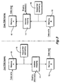
- FIG. 1 of the accompanying drawings is an illustration of such TDM framing. Since each channel in a single frame usually belongs to a different call, in order to route calls through a network it is necessary to be able to select or switch individual time-slots on one stream to the same or a different slot position on another stream, or to switch slots to a different position on the same stream. This function of TDM channel switching is central to telecom switch (exchange) operation. Devices which perform this routing are generally known as either crosspoint switches, or just switches.
- the switching can be implemented by integrated circuits which contain onboard memory, but for larger switches which are capable of switching large numbers of streams, the larger memory requirements result in the need to use additional memory devices to support the switching circuitry.
- a TDM switch has a number N of input streams and a number M of output streams, as shown in Figure 2 of the drawings.
- the number N of input streams may or may not be equal to the number M of output streams.
- a general non-blocking switch is one which has a number of streams, each of which may be arbitrarily allocated as an input or an output stream, and can route any channel on any input stream to any free channel on any output stream, regardless of the routing of other channels.
- a blocking switch does not have the resources to do this in every case, and certain combinations of routings will prevent some other routings from being made.
- the non-blocking switch is generally the preferred implementation as it offers more functionality.
- the core of a switching matrix is typically an area of memory. Assuming that an example of a square switch has N input streams and N output streams, each with T channels per TDM frame, one byte per channel and 8000 TDM frames per second, disregarding implementational efficiencies which can be gained, a simplified explanation of the functioning of such a switch follows, with reference to Figure 3 of the drawings which shows a technique of memory swapping.
- FIG. 3 there are provided two identical memory spaces (memory A and memory B) 10, 12.
- An address mapping circuit 14 receives routing information, and a sequential addressing circuit 16 provides addressing for both memory spaces.
- data from all N input streams is written to the memory A. This comprises N*T*8000 bytes per second. Therefore the memory A requires a write access time of 1/(N*T*8000) seconds per write cycle.
- the memory space 10 (memory A) is then swapped with the memory space 12 (memory B).
- the memory B is filled while the memory A is read out to fill the output channels.
- the output also comprises N*T channels, at N*T*8000 bytes per second.
- the memory also requires a read access time of 1/(N*T*8000) seconds per read cycle.
- the switching function is achieved by addressing the data in a suitable predetermined order to effect the necessary routing to the desired destination channels.
- this address manipulation may in principle be done either on read or write, but for one-to-many (for example, live feed) routing, the address manipulation must be done on output. In the example shown in Figure 3, the mapping is done on output.
- a non-blocking telecommunication circuit switch which produces multiple copies of input data in a reconfigurable memory with memory reconfiguration between write and read cycles providing multiple access to input data, thereby allowing multiple output data streams which can be multiplexed to the required output.
- the memory is written in one TDM interval, and read out in the following time interval.
- This principle is retained in the following solution; however the time available to read and write the memory can be increased at the expense of the amount of memory used. It will be shown that, by using a particular memory architecture, and increasing the total memory size by a multiplier K, the memory read and write bandwidth can be reduced by the same factor K. This principle can then be applied in order to design non-blocking switch matrices of arbitrary size, by trading off memory speed against the amount of memory required.
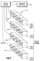
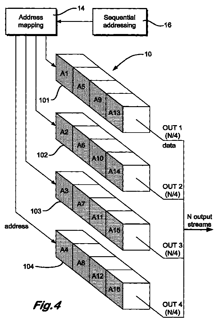
- FIG 4 there is shown a memory configuration for read cycles. This may, for example, be in the context of the memory space 10 (memory A) shown in Figure 3, and so similar reference numerals are used. It is assumed that the memory spaces 10 and 12 ( Figure 3) are increased in size by a factor of four. Furthermore, as shown in Figure 4, each memory space is divided into four banks 101 - 104 of four segments each. As shown, the segments for the memory space 10 (memory A) are referenced A1 - A16. Although not shown, the memory space 12 (memory B) has equivalent segments B1 - B16.
- Figure 4 shows 16 segments A1 - A16 of memory space 10 (memory A) being read in parallel.
- the memory is arranged so that each bank of four segments can be read independently from any of the other three banks.
- each of the four banks 101 -104 contains an identical version (or copy) of the data from all N input streams, thereby permitting non-blocking switching. How this is achieved is described later.
- the N output streams are divided into four equal groups OUT1 - OUT4, with N/4 streams in each group. Each of these groups of streams therefore requires a quarter of the total read bandwidth, and each stream group is filled from one of the four memory banks 101 - 104, as shown in Figure 4.
- the output stream group OUT1 can now be filled from the bank comprising the segments A1, A5, A9 and A13. Since this bank contains all the data from all of the N input streams, it therefore permits non-blocking switching. Address manipulation to achieve switch routing is the same as in respect of Figure 3.
- the amount of data to be read out to each stream group is ( (N/4)*T*8000 ) bytes, requiring 15.26 ns cycle time namely four times the cycle time previously described.
- the output stream groups OUT2 - OUT4 are filled in parallel from the remaining three banks 102 - 104 in the same manner.
- FIG. 5 there is shown a memory configuration for write cycles. Again, this is in the context of the memory space 10 (memory A).
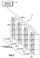
- Figure 5 shows the segments A1 - A16 being written in parallel.
- Figure 5 shows how the memory space can be filled from the N input streams to provide the four identical copies as described above in the context of Figure 4, while also reducing the memory write access constraint.
- the memory spaces are reconfigured, simply by switching of address, data and control lines, or by the use of dual port memory which permits alternative groupings of the memory segments without switching.
- the four memory banks which are arranged as contiguous rows for reading ( Figure 4) are rearranged as four contiguous columns 201 - 204 for writing. Simultaneously, the other memory space makes the opposite transition.
- the N input streams shown in Figure 5 are divided into four equal groups IN1 - IN4, with N/4 streams in each group.
- the stream group IN1 is written to memory segment A1.
- the amount of data to be written is ( (N/4) *T*8000 ) bytes, and therefore the memory access time is 15.26 ns (four times that described above).
- the group IN1 is also written to segments A2, A3 and A4. All these segments are in the same column bank 201 and can be written simultaneously with the same data.
- the group IN2 is similarly written to the column bank 202 including the segments A5 - A8, the group IN3 is written to the column bank 203 including the segments A9 - A12, and the group IN4 is written to the column bank 204 including the segments A13 - A16.
- the memory reconfiguration between row banks and column banks can be achieved simply by changing the connections of address, data and control lines to the memory. This can be achieved by the use of tri-state logic, for example, or by other techniques such as the use of dual port memory.
Landscapes
- Engineering & Computer Science (AREA)
- Computer Networks & Wireless Communication (AREA)
- Use Of Switch Circuits For Exchanges And Methods Of Control Of Multiplex Exchanges (AREA)
- Time-Division Multiplex Systems (AREA)
Abstract
Description
Claims (7)
- A non-blocking telecommunication circuit switch which produces multiple copies of input data in a reconfigurable memory (10) with memory reconfiguration between write and read cycles providing multiple access to input data, thereby allowing multiple output data streams (OUT1-OUT4) which can be multiplexed to the required output.
- A switch according to claim 1, wherein the memory (10) comprises memory segments (A1-A16) in matrix form, the memory segments being disposed in columns (201-204) and rows (101-104), memory writing and memory reading being configured to respective different ones of the columns (201-204) and rows (101-104).
- A switch according to claim 2, wherein identical data is written to a plurality of columns (201-204) or rows (101-104) of the memory (10), and data is read out from a plurality of rows (101-104) or columns (201-204) of the memory (10).
- A switch according to claim 2 or claim 3, wherein the number of memory segments (A1-A16) in a row (101-104) is equal to a number of memory segments (A1-A16) in a column (201-204).
- A switch according to claim 4, wherein the number of memory segments (A1-A16) in the rows (101-104) and columns (201-204) is a power of two.
- A switch according to claim 5, wherein the number of memory segments (A1-A16) in the rows (101-104) and columns (201-204) is four.
- A switch according to any one of the preceding claims, wherein the memory comprises two memory spaces (10,12), each being reconfigurable, reading from one memory space (e.g. 10) occurring during writing to the other memory space (e.g. 12).
Applications Claiming Priority (2)
| Application Number | Priority Date | Filing Date | Title |
|---|---|---|---|
| GB9917721A GB2352583B (en) | 1999-07-28 | 1999-07-28 | Telecommunication circuit switches |
| GB9917721 | 1999-07-28 |
Publications (2)
| Publication Number | Publication Date |
|---|---|
| EP1073309A2 true EP1073309A2 (en) | 2001-01-31 |
| EP1073309A3 EP1073309A3 (en) | 2005-05-25 |
Family
ID=10858094
Family Applications (1)
| Application Number | Title | Priority Date | Filing Date |
|---|---|---|---|
| EP00306077A Withdrawn EP1073309A3 (en) | 1999-07-28 | 2000-07-17 | A non-blocking circuit switch |
Country Status (2)
| Country | Link |
|---|---|
| EP (1) | EP1073309A3 (en) |
| GB (1) | GB2352583B (en) |
Cited By (4)
| Publication number | Priority date | Publication date | Assignee | Title |
|---|---|---|---|---|
| EP1585272A1 (en) * | 2004-04-05 | 2005-10-12 | Alcatel | Switching matrix for a telecommunication network element |
| EP1407362A4 (en) * | 2001-07-17 | 2007-01-24 | Alcatel Internetworking Inc | SWITCHING MATRIX WITH DUAL PORT MEMORY EMULATION DEVICE |
| US7450575B2 (en) * | 2004-02-17 | 2008-11-11 | Nec Electronics Corporation | Low redundancy data RAM architecture for monolithic time-space switches |
| CN1870833B (en) * | 2005-05-26 | 2010-12-08 | 中兴通讯股份有限公司 | A method for realizing large-capacity non-blocking time-division switching network and its single-board device |
Family Cites Families (5)
| Publication number | Priority date | Publication date | Assignee | Title |
|---|---|---|---|---|
| IT1149253B (en) * | 1980-09-09 | 1986-12-03 | Sits Soc It Telecom Siemens | SWITCHING NETWORK FOR PCM CHANNELS |
| US4736361A (en) * | 1984-12-28 | 1988-04-05 | Gte Laboratories Incorporated | Digital switching system with two-directional addressing rams |
| JPH0779514B2 (en) * | 1986-01-24 | 1995-08-23 | 日本電気株式会社 | Time division time switch control method |
| US5796733A (en) * | 1996-07-03 | 1998-08-18 | General Signal Corporation | Time division switching system |
| US6170046B1 (en) * | 1997-10-28 | 2001-01-02 | Mmc Networks, Inc. | Accessing a memory system via a data or address bus that provides access to more than one part |
-
1999
- 1999-07-28 GB GB9917721A patent/GB2352583B/en not_active Expired - Fee Related
-
2000
- 2000-07-17 EP EP00306077A patent/EP1073309A3/en not_active Withdrawn
Cited By (5)
| Publication number | Priority date | Publication date | Assignee | Title |
|---|---|---|---|---|
| EP1407362A4 (en) * | 2001-07-17 | 2007-01-24 | Alcatel Internetworking Inc | SWITCHING MATRIX WITH DUAL PORT MEMORY EMULATION DEVICE |
| US7450575B2 (en) * | 2004-02-17 | 2008-11-11 | Nec Electronics Corporation | Low redundancy data RAM architecture for monolithic time-space switches |
| EP1585272A1 (en) * | 2004-04-05 | 2005-10-12 | Alcatel | Switching matrix for a telecommunication network element |
| US7447199B2 (en) | 2004-04-05 | 2008-11-04 | Alcatel | Switching matrix for a telecommunication network element |
| CN1870833B (en) * | 2005-05-26 | 2010-12-08 | 中兴通讯股份有限公司 | A method for realizing large-capacity non-blocking time-division switching network and its single-board device |
Also Published As
| Publication number | Publication date |
|---|---|
| GB2352583B (en) | 2003-12-10 |
| GB2352583A (en) | 2001-01-31 |
| GB9917721D0 (en) | 1999-09-29 |
| EP1073309A3 (en) | 2005-05-25 |
Similar Documents
| Publication | Publication Date | Title |
|---|---|---|
| US5091903A (en) | Switching network and switching-network module for an atm system | |
| US5576873A (en) | Telecommunications switch architecture | |
| EP0363053B1 (en) | Asynchronous time division switching arrangement and a method of operating same | |
| US7009964B2 (en) | Rotator switch data path structures | |
| EP0256701B1 (en) | Crosspoint circuitry for data packet space division switches | |
| US6144662A (en) | Fast routing and non-blocking switch which accomodates multicasting and variable length packets | |
| US5355372A (en) | Threshold-based load balancing in ATM switches with parallel switch planes related applications | |
| EP1450524B1 (en) | Circulating switch | |
| US8923288B2 (en) | Multi-service transport apparatus with switch for integrated transport networks | |
| EP0274800A1 (en) | Multistage switching system for switching N1 input channels to N2 output channels | |
| EP1699257B1 (en) | Switch for integrated telecommunication networks. | |
| JPH05502356A (en) | Multiplexing switch | |
| JP3105614B2 (en) | Light exchange matrix | |
| JP2004534443A (en) | Single-stage switch structure | |
| NL8600613A (en) | WIDEBAND SPACE SWITCH NETWORK AND PARALLEL SERIES CONVERTER AND SERIES PARALLEL CONVERTER FOR APPLICATION IN SUCH SPACE SWITCH NETWORK. | |
| JPH0646469A (en) | Reconstitutible switching memory | |
| GB2352583A (en) | Telecommunication circuit switches | |
| US6680939B1 (en) | Expandable router | |
| JP3103298B2 (en) | ATM switch address generation circuit | |
| US5257260A (en) | Expanding switching capability of a time division communication system by multiplexing groups of circuits into successions | |
| US5546393A (en) | Asynchronous transfer mode data cell routing device for a reverse omega network | |
| US6208641B1 (en) | Switch with one-bit resolution | |
| EP0116386B1 (en) | Time division switching system | |
| US7447199B2 (en) | Switching matrix for a telecommunication network element | |
| EP0446492B1 (en) | Communication switching module |
Legal Events
| Date | Code | Title | Description |
|---|---|---|---|
| PUAI | Public reference made under article 153(3) epc to a published international application that has entered the european phase |
Free format text: ORIGINAL CODE: 0009012 |
|
| AK | Designated contracting states |
Kind code of ref document: A2 Designated state(s): AT BE CH CY DE DK ES FI FR GB GR IE IT LI LU MC NL PT SE |
|
| AX | Request for extension of the european patent |
Free format text: AL;LT;LV;MK;RO;SI |
|
| PUAL | Search report despatched |
Free format text: ORIGINAL CODE: 0009013 |
|
| AK | Designated contracting states |
Kind code of ref document: A3 Designated state(s): AT BE CH CY DE DK ES FI FR GB GR IE IT LI LU MC NL PT SE |
|
| AX | Request for extension of the european patent |
Extension state: AL LT LV MK RO SI |
|
| RIC1 | Information provided on ipc code assigned before grant |
Ipc: 7H 04L 12/56 B Ipc: 7H 04Q 11/04 A |
|
| AKX | Designation fees paid | ||
| REG | Reference to a national code |
Ref country code: DE Ref legal event code: 8566 |
|
| STAA | Information on the status of an ep patent application or granted ep patent |
Free format text: STATUS: THE APPLICATION IS DEEMED TO BE WITHDRAWN |
|
| 18D | Application deemed to be withdrawn |
Effective date: 20060223 |