EP1073205A2 - Dual-band high-frequency transmission mixer having two outputs - Google Patents
Dual-band high-frequency transmission mixer having two outputs Download PDFInfo
- Publication number
- EP1073205A2 EP1073205A2 EP00116406A EP00116406A EP1073205A2 EP 1073205 A2 EP1073205 A2 EP 1073205A2 EP 00116406 A EP00116406 A EP 00116406A EP 00116406 A EP00116406 A EP 00116406A EP 1073205 A2 EP1073205 A2 EP 1073205A2
- Authority
- EP
- European Patent Office
- Prior art keywords
- frequency
- output
- local
- input
- band
- Prior art date
- Legal status (The legal status is an assumption and is not a legal conclusion. Google has not performed a legal analysis and makes no representation as to the accuracy of the status listed.)
- Withdrawn
Links
Images


Classifications
-
- H—ELECTRICITY
- H03—ELECTRONIC CIRCUITRY
- H03D—DEMODULATION OR TRANSFERENCE OF MODULATION FROM ONE CARRIER TO ANOTHER
- H03D7/00—Transference of modulation from one carrier to another, e.g. frequency-changing
- H03D7/14—Balanced arrangements
- H03D7/1425—Balanced arrangements with transistors
- H03D7/1483—Balanced arrangements with transistors comprising components for selecting a particular frequency component of the output
-
- H—ELECTRICITY
- H03—ELECTRONIC CIRCUITRY
- H03D—DEMODULATION OR TRANSFERENCE OF MODULATION FROM ONE CARRIER TO ANOTHER
- H03D7/00—Transference of modulation from one carrier to another, e.g. frequency-changing
- H03D7/14—Balanced arrangements
- H03D7/1425—Balanced arrangements with transistors
- H03D7/1433—Balanced arrangements with transistors using bipolar transistors
-
- H—ELECTRICITY
- H03—ELECTRONIC CIRCUITRY
- H03D—DEMODULATION OR TRANSFERENCE OF MODULATION FROM ONE CARRIER TO ANOTHER
- H03D7/00—Transference of modulation from one carrier to another, e.g. frequency-changing
- H03D7/14—Balanced arrangements
- H03D7/1425—Balanced arrangements with transistors
- H03D7/1475—Subharmonic mixer arrangements
Definitions
- This invention relates to a dual-band output switching high-frequency transmission circuit and, more particularly, to a transmission mixer for use in a dual-band portable equipment to convert an intermediate frequency into a transmission frequency.
- a dual-band portable equipment which uses two radio frequency bands such as 900MHz and 1.8GHz in the manner which are represented in GSM900/DCS-1800.
- a transmission mixer for use in the dual-band portable equipment a conventional mixer is assigned with a band because the conventional mixer has only one output in the manner which will later be described in conjunction with Fig. 1.
- a circuit for generating jitter includes a mixer which mixes a jittered signal from a jitter generator with the output of a variable frequency oscillator to produce a broadband jittered output.
- a preferred form of the circuit uses a double frequency translation technique in which the output from a frequency oscillator is applied to a jitter generator and to a first frequency translation device to translate a variable input frequency to an intermediate frequency. The jittered signal and the intermediate frequency signal are then applied to a second frequency translation device to produce a jittered output at the variable input frequency.
- JP-A 5-244032 describes "DUAL-BAND RADIO COMMUNICATION APPARATUS" to increase circuits which can be shared and reduce the size of the apparatus by converting an IF signal into a radio signal of a first or second band with common local oscillation signal consisting of an intermediate frequency of a transmission radio frequency.
- a fundamental wave consisting of the intermediate frequency of a frequency synthesizer is outputted as a common local oscillation signal to a mixer.
- a first transmitting band pass filter circuit extracts the signal of the first band from the converted signal and sends it.
- a second transmitting band pass filter circuit extracts the signal of the second band from the converted signal and sends it. Then the received signals are inputted by an antenna selector to first and second receiving band pass filter circuits. The received signal is converted down by being multiplied by the local oscillation signal of a frequency synthesizer so that it is converted to a first reception IF frequency by a mixer. Thus, the circuits which can be shared are increased to reduce the size of the apparatus.
- European patent Publication No. 653851 or EP A 653851 discloses a radio communication apparatus of multi-band which is suitable to radio frequency bands which are relatively apart from each other. That is, the radio communication apparatus according to EP A 653851 comprises a common oscillator having an oscillation frequency which is selected so as to become about middle between a first frequency band and a second frequency band.
- JP-A 8-223,073 or JP-A 8-233073 discloses a heterodyne "DUAL BAND RADIO COMMUNICATION EQUIPMENT" which is used in common in two bands like 800MHz band and 1.5GHz band in a digital land mobile radiotelephone. That is, in JP-A 8-223073, a reception intermediate frequency is made equal to a transmission/reception frequency difference between first and second radio frequency bands, and a frequency of a transmission intermediate frequency signal is set to two-fold frequency of the transmission/reception frequency difference.
- the dual band radio communication equipment comprises a first local oscillating circuit for oscillating a first local oscillation signal for converting a received signal of the first radio frequency band into a received intermediate frequency signal, a second local oscillating circuit for oscillating a second local oscillation signal for converting a received signal of the second radio frequency band into a received intermediate frequency signal, a first switch for performing switching between the first and the second local oscillation signals to produce a selected local oscillation signal which is supplied to a reception mixer, and a second switch for performing switching between the first or the second local oscillation signal and a third local oscillation signal.
- the second switch produces an output signal which is supplied to a transmission mixer for multiplying the output signal by the transmission intermediate frequency signal to produce a transmission signal having a prescribed frequency band of the first radio frequency band and a transmission signal having a prescribed frequency band of the second radio frequency band.
- JP-A 10-107676 discloses "COMMUNICATING APPARATUS" which corresponds to a dual band in which the frequency intervals between a transmitting band and a receiving band are different from each other and also makes this apparatus small, light, inexpensive and which also is low power consumption by setting the frequency of a voltage-controlled offset signal oscillator (offset VCO) so that it may be equal to the difference of intervals between transmitting band and receiving band.
- offset VCO voltage-controlled offset signal oscillator
- the communication apparatus disclosed in JP-A 10-107676 appropriately combines an offset VCO, a first high frequency VCO and a second high frequency VCO and generates a high frequency that is needed for transmission and receiving.
- the difference of the two transmitting band and receiving band is set to be equal. Thereby, a high frequency signal that is needed for the transmission and receiving of the dual band can be created with minimum block structure.
- the frequency of an IF signal becomes equal in either case of two receiving bands, the structure of a receiving system after a receiving mixer can be simplified, and it is possible to make this apparatus light and be low power consumption.
- a conventional dual-band output switching high-frequency transmission circuit is disadvantageous in that two transmission mixers becomes a necessity or an external switch for switching output frequency matching circuits or the like becomes a necessity extra.
- this invention adopts technical structure as follows. That is, this invention provides a circuit combining a following five items in order to simplify structure:
- a transmission mixer is for use in a dual-band portable equipment to convert an intermediate frequency into a transmission frequency.
- the above-understood transmission mixer has a local input port supplied with a local signal having a local frequency from a local oscillator, an intermediate input port supplied with an input signal having an input frequency which is equal to the intermediate frequency, a first output port for producing a first output signal having a first output frequency, and a second output port for producing a second output signal having a second output frequency which is different from the first output frequency.
- the first and the second output ports are connected to first and second loads, respectively, the first load is that where impedance-matching is made at the first output frequency, and the second load is that where impedance-matching is made at the second output frequency.
- the above-mentioned transmission mixer desirably may have a power-supply terminal applied with a power-supply voltage and a ground terminal having a ground potential and the transmission mixer may comprise a first npn-type bipolar transistor having a base electrode connected to the local input terminal, a collector electrode connected to the power-supply terminal through the first load, and an emitter electrode connected to a common node, a second npn- type bipolar transistor having a collector electrode connected to the power-supply terminal through the load and an emitter electrode connected to the common node, a third npn-type bipolar transistor having a collector electrode connected to the common node and an emitter electrode connected to the ground terminal, a first output capacitor connected between the collector terminal of the first npn-type bipolar transistor and the first output port, a second output capacitor connected between the collector terminal of the second npn-type bipolar transistor and the second output port, a capacitor connected between a base electrode of the second npn-type bipolar transistor,
- the above-understood dual-band output switching high-frequency transmission circuit comprises a first local oscillator for oscillating a first local signal having a first local frequency, a second local oscillator for oscillating a second local signal having a second local frequency which is different from the first local frequency, a transmission mixer having a local input port selectively supplied with one of the first and the second local signals, an intermediate input port supplied with an input signal having an input frequency of an intermediate frequency, and first and second output ports for producing first and second output signals having first and second output frequencies which are different from each other, a first band pass filter connected to the first output port and having a pass band of the first output frequency, and a second band pass filter connected to the second output port and having a pass band of the second output frequency.
- the first and the second local frequencies may be lower than the first and the second output frequencies, respectively, the first output frequency may be equal to that obtained by adding the input frequency to the first local frequency, and the second output frequency may be equal to that obtained by adding the input frequency to the second local frequency.
- the first and the second local frequencies may be higher than the first and the second output frequencies, respectively, the first output frequency may be equal to that obtained by subtracting the input frequency from the first local frequency, and the second output frequency may be equal to that obtained by subtracting the input frequency from the second local frequency.
- the first local frequency may be higher than the first output frequency
- the second local frequency may be lower than said second output frequency
- the first output frequency may be equal to that obtained by subtracting the input frequency from the first local frequency
- the second output frequency may be equal to that obtained by adding the input frequency to the second local frequency.
- the first local frequency may be lower than the first output frequency
- the second local frequency may be higher than the second output frequency
- the first output frequency may be equal to that obtained by adding the input frequency to the first local frequency
- the second output frequency may be equal to that obtained by subtracting the input frequency from the second local frequency.
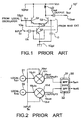
- the illustrated transmission mixer 10' is a one-output mixer.
- the transmission mixer 10' has a local input port 10 LO supplied with a local signal having a local frequency f LO from a local oscillator (which is not shown in Fig. 1 and which will later become clear), an intermediate input port 10 in supplied with an input signal having an input frequency f in of an intermediate frequency, and an output port 10 out for producing an output signal having an output frequency f out .
- the output port 10 out is connected to a load LD.
- the load LD is used that where impedance-matching is made at the output frequency f out .
- the transmission mixer 10' has a power-supply terminal 10 PW applied with a power-supply voltage Vcc and a ground terminal 10 gd having a ground potential.
- the transmission mixer 10' comprises first through third npn-type bipolar transistor Q1, Q2, Q3, an output capacitor C out , a capacitor C, and an input capacitor C in .
- the first npn-type bipolar transistor Q1 has a base electrode connected to the local input terminal 10 LO , a collector electrode which is directly connected to the power-supply terminal 10 PW , and an emitter electrode connected to a common node N.
- the second npn-type bipolar transistor Q2 has a collector electrode connected to the power-supply terminal 10PW through the load LD and an emitter electrode connected to the common node N.
- the third npn-type bipolar transistor Q3 has a collector electrode connected to the common node N and an emitter electrode connected to the ground terminal 10 gd .
- the output capacitor C out is connected between the collector electrode of the second npn-type bipolar transistor Q2 and the output port 10out.
- the capacitor C is connected between a base electrode of the npn-type bipolar transistor Q2 and the ground terminal 10 gd .
- the input capacitor C in is connected between a base electrode of the third npn-type bipolar transistor Q3 and the intermediate input port 10 in .
- the base electrodes of the first through the third npn-type bipolar transistor Q1 to Q3 are supplied to a bias voltage from a bias circuit (not shown).
- Fig. 2 shows a first conventional dual-band output switching high-frequency transmission circuit.
- the illustrated dual-band output switching high-frequency transmission circuit comprises first and second local oscillators 21 and 22, first and second transmission mixers 10'-1 and 10'-2, and first and second band pass filters (BPFs) 31 and 32.
- the first local oscillator 21 oscillates a first local signal having a first local frequency fLO1.
- the second local oscillator 22 oscillates a second local signal having a second local frequency fLO2 which is different from the first local frequency fLO1.
- the first transmission mixer 10'-1 has a first local input port 10LO1 supplied with the first local signal, a first intermediate input port 10in1 supplied with an input signal having an input frequency fin which is equal to an intermediate frequency, and a first output port for producing a first output signal having a first output frequency fout1.
- the second transmission mixer 10'-2 has a second local input port 10LO2 supplied with the second local signal, a second intermediate input port 10in2 supplied with the input signal having the input frequency fin of the intermediate frequency, and a second output port 10out2 for producing a second output signal having a second output frequency fout2.
- the first band pass filter 31 has a pass band for the first output frequency fout1.
- the second band pass filter 32 has a pass band for the second output frequency fout2.
- Fig. 3 shows a second conventional dual-band output switching high-frequency transmission circuit.
- the illustrated dual-band output switching high-frequency transmission circuit comprises not only the first and the second local oscillators 21 and 22, the transmission mixer (the one-output mixer) 10', and the first and the second band pass filters (BPFs) 31 and 32 but also first and second buffers 41 and 42 and an external switch 50.
- BPFs band pass filters
- the first buffer 41 is disposed between the output port 10out of the transmission mixer 10' and the first band pass filter 31 while the second buffer 42 is disposed between the output port 10out of the transmission mixer 10' and the second band pass filter 32.
- an output frequency matching circuit (impedance-matching LC circuit) may be used in lieu of the buffer.
- the second conventional dual-band output switching high-frequency transmission circuit is composed so that the output frequency matching circuits or the buffers 41 and 42 are switched by the external switch 50.
- the above-mentioned device in the dual-band portable equipment, the above-mentioned device must be made in a case of using the conventional one-output mixer 10' because the band pass filters of the output stage have the two inputs.
- Fig. 4 is a circuit diagram showing a two-output mixer which is the transmission mixer 10 according to this invention.
- the illustrated transmission mixer (two-output mixer) is for use in a dual-band portable equipment to convert an intermediate frequency into a transmission frequency and has a structure having two output ports in which a collector output of each differential transistor in a balance-type mixer is connected to a load. The respective outputs are called a first output 1 and a second output 2.
- the output of each mixer is assigned with each frequency port.
- the first output frequency 1 (fout1) is assigned with the first output 1 while the second output frequency 1 (fout2) is assigned with the second output 2.
- the transmission mixer 10 has a local input port 10 LO supplied with a local signal having a local frequency f LO from a local oscillator (not shown), an intermediate input port 10 in supplied with an input signal having art input frequency f in of the intermediate frequency, a first output port 10 out1 for producing a first output signal having a first output frequency f out1 , and a second output port 10 out2 for producing a second output signal having a second output frequency f out2 which is different from the first output frequency f out1 .
- the first and the second output ports 10out1 and 10out2 are connected to first and second loads LD1 and LD2, respectively.
- the first load LD1 is that where impedance-matching is made at the first output frequency f out1 while the second load LD2 is that where impedance-matching is made at the second output frequency f out2 .
- optimization is made so that a value of an inductor serving as the load for each output and a value of a capacitor connected thereto in series are impedance matched at each frequency. That is, the first output 1 has an optimized impedance at the first output frequency fout1 while the second output 2 has an optimized impedance at the second output frequency fout2.
- the transmission mixer 10 has a power-supply terminal 10 PW applied with a power-supply voltage Vcc and a ground terminal 10 gd having a ground potential.
- the transmission mixer 10 comprises first through third npn-type bipolar transistors Q1, Q2, Q3, first and second output capacitors C out1 and C out2 , a capacitor C, and an input capacitor C in .
- the first npn-type bipolar transistor Q1 has a base electrode connected to the local input port 10 LO , a collector electrode connected to the power-supply electrode 10 PW through the first load LD1, and an emitter electrode connected to a common node N.
- the second npn-type bipolar transistor Q2 has a collector electrode connected to the power-supply terminal 10 PW through the second load LD2 and an emitter electrode connected to the common node N.
- the third npn-type bipolar transistor Q3 has a collector electrode connected to the common node N and an emitter electrode connected to the ground terminal
- the first output capacitor C out1 is connected between the collector electrode of the first npn-type bipolar transistor Q1 and the first output port 10 out1 .
- the second output capacitor C out2 is connected to the collector electrode of the second npn-type bipolar transistor Q2 and the second output port 10 out2 .
- the capacitor C is connected between a base electrode of the second npn-type bipolar transistor Q2 and the ground terminal 10 gd .
- the input capacitor C in is connected between a base electrode of the third npn-type bipolar transistor Q3 and the intermediate input port 10 in .
- the base electrodes of the first through the third npn-type bipolar transistors Q1 through Q3 are supplied with a bias voltage from a bias circuit (not shown).
- Fig. 5 shows a dual-band output switching high-frequency transmission circuit for use in a dual-band portable equipment that is capable of switching frequencies of two bands by using the transmission mixer (two-output mixer) 10 illustrated in Fig. 4.
- the illustrated dual-band output switching high-frequency transmission circuit comprises the first and the second local oscillators 21 and 22, the transmission mixer 10, and the first and the second band pass filter (BPSs) 31 and 32.
- the first local oscillator 21 oscillates the first local signal having the first local frequency f LO1 .
- the second local oscillator 22 oscillates the second local signal having the second local frequency f LO2 which is different from the first local frequency f LO1 .
- the transmission mixer 10 has the local input ports 10 LO supplied with the first or the second local signals, the intermediate input port 10 in supplied with the input signal having the input frequency f in of the intermediate frequency, first and second output ports 10 out1 and 10 out2 for producing the first and the second output signals having the first and the second output frequencies f out1 and f out2 which are different from each other.
- the first band pass filter 31 has the pass band for the first output frequency f out1 .
- the second band pass filter 32 has the pass band for the second output frequency f out2 .
- the illustrated dual-band output switching high-frequency transmission circuit is a lower local system where the local frequency is lower than a radio transmission output frequency. That is, it will be assumed that the first and the second local frequencies f out1 and f out2 are lower than the first and the second output frequencies f out1 and f out2 , respectively.
- the above-mentioned equations means that the two output frequencies f out1 and f out2 are switched by switching the local frequencies.
- the first output 1 has a large output level and the second output 2 has a small output level for the first output frequency f out1 when the first output frequency f out1 is selected as the output frequency.
- the second output frequency f out2 is selected as the output frequency
- the second output 2 has a large output level while the first output 1 has a small output level for the second output frequency f out2 .
- frequency structure may be modified to an upper local system in which the local frequencies are higher than the radio transmission output frequencies. That is, the first and the second local frequencies f LO1 and f LO2 may be higher than the first and the second output frequencies f out1 and f out2 , respectively.
- the first local frequency f LO1 may be higher than the first output frequency f out1 and the second local frequency f LO2 may be lower than the second output frequency f out2 .
- the first local frequency f LO1 may be lower than the first output frequency f out1 while the second local frequency f LO2 may be higher than the second output frequency f out2 .
- the first output frequency f out1 is equal to that obtained by adding the input frequency f in to the first local frequency f LO1
Landscapes
- Engineering & Computer Science (AREA)
- Power Engineering (AREA)
- Transmitters (AREA)
- Transceivers (AREA)
- Superheterodyne Receivers (AREA)
Abstract
Description
Claims (12)
- A transmission mixer for use in a dual band portable equipment to convert an intermediate frequency into a transmission frequency, said transmission mixer having:a local input port supplied with a local signal having a local frequency from a local oscillator;an intermediate input port supplied with an input signal having an input frequency which is equal to the intermediate frequency;a first output port for producing a first output signal having a first output frequency; anda second output port for producing a second output signal having a second output frequency which is different from the first output frequency.
- A transmission mixer as claimed in claim 1, wherein said first and said second output ports are connected to first and second loads, respectively, said first load being that where impedance-matching is made at said first output frequency, said second load being that where impedance-matching is made at said second output frequency.
- A transmission mixer as claimed in claim 2, said transmission mixer having a power-supply terminal applied with a power-supply voltage and a ground terminal having a ground potential, wherein said transmission mixer comprises:a first npn-type bipolar transistor having a base electrode connected to said local input terminal, a collector electrode connected to said power-supply terminal through said first load, and an emitter electrode connected to a common node;a second npn-type bipolar transistor having a collector electrode connected to said power-supply terminal through said load and an emitter electrode connected to the common node;a third npn-type bipolar transistor having a collector electrode connected to the common node and an emitter electrode connected to said ground terminal;a first output capacitor connected between the collector terminal of said first npn-type bipolar transistor and said first output port;a second output capacitor connected between the collector terminal of said second npn-type bipolar transistor and said second output port;a capacitor connected between a base electrode of said second npn-type bipolar transistor and said ground terminal; andan input capacitor connected between a base electrode of said third npn-type bipolar transistor and said intermediate input terminal.
- A transmission mixer as claimed in claim 3, wherein the base terminals of said first through said third npn-type bipolar transistors are supplied with a bias voltage from a bias circuit.
- A dual-band output switching high-frequency transmission circuit for use in a dual-band portable equipment, said dual-band output switching high-frequency transmission circuit comprising:a first local oscillator for oscillating a first local signal having a first local frequency;a second local oscillator for oscillating a second local signal having a second local frequency which is different from the first local frequency;a transmission mixer having a local input port selectively supplied with one of said first and said second local signals, an intermediate input port supplied with an input signal having an input frequency of an intermediate frequency, and first and second output ports for producing first and second output signals having first and second output frequencies which are different from each other;a first band pass filter connected to said first output port and having a pass band of said first output frequency; anda second band pass filter connected to said second output port and having a pass band of said second output frequency.
- A dual-band output switching high-frequency transmission circuit as claimed in claim 5, wherein:said first and said second local frequencies are lower than said first and said second output frequencies, respectively;said first output frequency being equal to that obtained by adding said input frequency to said first local frequency; andsaid second output frequency being equal to that obtained by adding said input frequency to said second local frequency.
- A dual-band output switching high-frequency transmission circuit as claimed in claim 5, wherein:said first and said second local frequencies are higher than said first and said second output frequencies, respectively;said first output frequency being equal to that obtained by subtracting said input frequency from said first local frequency; andsaid second output frequency being equal to that obtained by subtracting said input frequency from said second local frequency.
- A dual-band output switching high-frequency transmission circuit as claimed in claim 5, wherein:said first local frequency is higher than said first output frequency;said second local frequency being lower than said second output frequency;said first output frequency being equal to that obtained by subtracting said input frequency from said first local frequency; andsaid second output frequency being equal to that obtained by adding said input frequency to said second local frequency.
- A dual-band output switching high-frequency transmission circuit as claimed in claim 5, wherein:said first local frequency is lower than said first output frequency;said second local frequency being higher than said second output frequency;said first output frequency being equal to that obtained by adding said input frequency to said first local frequency; andsaid second output frequency being equal to that obtained by subtracting said input frequency from said second local frequency.
- A dual-band output switching high-frequency transmission circuit as claimed in claim 5, wherein said first and said second output ports are connected to first and second loads, respectively, said first load being that where impedance-matching is made at said first output frequency, said second load being that where impedance-matching is made at said second output frequency.
- A dual-band output switching high-frequency transmission circuit as claimed in claim 10, said transmission mixer having a power-supply terminal applied with a power-supply voltage and a ground terminal having a ground potential, wherein said transmission mixer comprises:a first npn-type bipolar transistor having a base electrode connected to said local input terminal, a collector electrode connected to said power-supply terminal through said first load, and an emitter electrode connected to a common node;a second npn-type bipolar transistor having a collector electrode connected to said power-supply terminal through said load and an emitter electrode connected to the common node;a third npn-type bipolar transistor having a collector electrode connected to the common node and an emitter electrode connected to said ground terminal;a first output capacitor connected between the collector terminal of said first npn-type bipolar transistor and said first output port;a second output capacitor connected between the collector terminal of said second npn-type bipolar transistor and said second output port;a capacitor connected between a base electrode of said second npn-type bipolar transistor and said ground terminal; andan input capacitor connected between a base electrode of said third npn-type bipolar transistor and said intermediate input terminal.
- A dual-band output switching high-frequency transmission circuit as claimed in claim 11, wherein the base terminals of said first through said third npn-type bipolar transistors are supplied with a bias voltage from a bias circuit.
Applications Claiming Priority (2)
| Application Number | Priority Date | Filing Date | Title |
|---|---|---|---|
| JP11217462A JP2001044858A (en) | 1999-07-30 | 1999-07-30 | Transmission mixer and two-band output changeover highfrequency transmission circuit |
| JP21746299 | 1999-07-30 |
Publications (2)
| Publication Number | Publication Date |
|---|---|
| EP1073205A2 true EP1073205A2 (en) | 2001-01-31 |
| EP1073205A3 EP1073205A3 (en) | 2003-07-02 |
Family
ID=16704622
Family Applications (1)
| Application Number | Title | Priority Date | Filing Date |
|---|---|---|---|
| EP00116406A Withdrawn EP1073205A3 (en) | 1999-07-30 | 2000-07-28 | Dual-band high-frequency transmission mixer having two outputs |
Country Status (3)
| Country | Link |
|---|---|
| US (1) | US6640091B1 (en) |
| EP (1) | EP1073205A3 (en) |
| JP (1) | JP2001044858A (en) |
Cited By (3)
| Publication number | Priority date | Publication date | Assignee | Title |
|---|---|---|---|---|
| DE10245609A1 (en) * | 2002-09-30 | 2004-04-29 | Advanced Micro Devices, Inc., Sunnyvale | mixing device |
| US7324799B2 (en) | 2003-06-10 | 2008-01-29 | Nokia Corporation | Multiband mixer |
| CN101867347B (en) * | 2009-04-15 | 2012-12-12 | 中国科学院电子学研究所 | Power amplifier circuit with reconfigurable frequency band in multi-band wireless mobile communication system |
Families Citing this family (8)
| Publication number | Priority date | Publication date | Assignee | Title |
|---|---|---|---|---|
| US6950478B1 (en) * | 2001-08-02 | 2005-09-27 | Texas Instruments Incorporated | Transmitter and method having a low sampling frequency for digital to analog conversion |
| JP2003152815A (en) | 2001-11-14 | 2003-05-23 | Hitachi Ltd | Communication semiconductor integrated circuit |
| US7522898B2 (en) * | 2005-06-01 | 2009-04-21 | Wilinx Corporation | High frequency synthesizer circuits and methods |
| US7415257B2 (en) * | 2005-10-14 | 2008-08-19 | Kuei-ann Wen | Dual-band mixer and its design flow |
| US7894778B2 (en) * | 2006-06-30 | 2011-02-22 | Broadcom Corporation | LO generator to reject unwanted sideband |
| JP4357547B2 (en) * | 2007-06-13 | 2009-11-04 | 株式会社東芝 | Modulation circuit |
| CN101816129B (en) * | 2007-08-10 | 2015-03-25 | 皇家飞利浦电子股份有限公司 | Multiple transmission apparatus with reduced coupling |
| US8665016B2 (en) * | 2012-04-30 | 2014-03-04 | Broadcom Corporation | Supply tracking |
Family Cites Families (20)
| Publication number | Priority date | Publication date | Assignee | Title |
|---|---|---|---|---|
| JPS5919355B2 (en) * | 1977-10-26 | 1984-05-04 | ヤマハ株式会社 | electronic musical instruments |
| JPH0642614B2 (en) * | 1987-06-11 | 1994-06-01 | 株式会社日立製作所 | Mixer circuit |
| EP0345390A1 (en) | 1988-06-08 | 1989-12-13 | Hewlett-Packard Limited | Improvement in or Relating to Jitter Circuits |
| JPH0478202A (en) | 1990-07-18 | 1992-03-12 | Toshiba Corp | Frequency mixer circuit |
| JP3086512B2 (en) * | 1990-11-14 | 2000-09-11 | エリクソン−ジーイー モービル コミュニケーションズ ホールディング インコーポレイテッド | Transmitter and its power amplifier circuit |
| JP2840496B2 (en) | 1992-02-26 | 1998-12-24 | 三洋電機株式会社 | Dual band wireless communication device |
| JPH0653753A (en) * | 1992-07-29 | 1994-02-25 | Nec Corp | Power amplifier |
| JP3307991B2 (en) * | 1992-09-09 | 2002-07-29 | 富士通株式会社 | Mobile communication terminal |
| JPH06343041A (en) | 1993-06-01 | 1994-12-13 | Nippon Telegr & Teleph Corp <Ntt> | Synthesizer circuit |
| DE4338721A1 (en) | 1993-11-12 | 1995-05-18 | Philips Patentverwaltung | Multi-band radio |
| JPH08223065A (en) | 1995-02-13 | 1996-08-30 | Toshiba Corp | Frequency converter |
| JPH08223073A (en) | 1995-02-14 | 1996-08-30 | Fujitsu Ltd | Dual band wireless communication device |
| JP3189633B2 (en) * | 1995-07-25 | 2001-07-16 | 株式会社村田製作所 | Mixer |
| EP0774850B1 (en) * | 1995-11-16 | 2004-10-27 | Ntt Mobile Communications Network Inc. | Digital signal detecting method and detector |
| JPH10107676A (en) | 1996-08-08 | 1998-04-24 | Asahi Chem Ind Co Ltd | Communication device |
| JP3255054B2 (en) * | 1996-12-10 | 2002-02-12 | 富士通株式会社 | Digital mobile phone |
| GB2320631B (en) * | 1996-12-23 | 2001-07-18 | Nokia Mobile Phones Ltd | Radio receiver and radio transmitter |
| US5884149A (en) * | 1997-02-13 | 1999-03-16 | Nokia Mobile Phones Limited | Mobile station having dual band RF detector and gain control |
| US5983082A (en) * | 1997-10-31 | 1999-11-09 | Motorola, Inc. | Phase quadrature signal generator having a variable phase shift network |
| JPH11205173A (en) * | 1998-01-12 | 1999-07-30 | Alps Electric Co Ltd | Receiver for data transmission |
-
1999
- 1999-07-30 JP JP11217462A patent/JP2001044858A/en active Pending
-
2000
- 2000-07-28 EP EP00116406A patent/EP1073205A3/en not_active Withdrawn
- 2000-07-28 US US09/628,554 patent/US6640091B1/en not_active Expired - Fee Related
Cited By (5)
| Publication number | Priority date | Publication date | Assignee | Title |
|---|---|---|---|---|
| DE10245609A1 (en) * | 2002-09-30 | 2004-04-29 | Advanced Micro Devices, Inc., Sunnyvale | mixing device |
| US6937849B2 (en) | 2002-09-30 | 2005-08-30 | Advanced Micro Devices, Inc. | Mixing apparatus |
| DE10245609B4 (en) * | 2002-09-30 | 2014-01-02 | Advanced Micro Devices, Inc. | mixing device |
| US7324799B2 (en) | 2003-06-10 | 2008-01-29 | Nokia Corporation | Multiband mixer |
| CN101867347B (en) * | 2009-04-15 | 2012-12-12 | 中国科学院电子学研究所 | Power amplifier circuit with reconfigurable frequency band in multi-band wireless mobile communication system |
Also Published As
| Publication number | Publication date |
|---|---|
| EP1073205A3 (en) | 2003-07-02 |
| US6640091B1 (en) | 2003-10-28 |
| JP2001044858A (en) | 2001-02-16 |
Similar Documents
| Publication | Publication Date | Title |
|---|---|---|
| US7567610B2 (en) | Frequency conversion circuit, radio frequency wave receiver, and radio frequency transceiver | |
| US6057714A (en) | Double balance differential active ring mixer with current shared active input balun | |
| US6366166B1 (en) | Double pass band amplifier circuit and a radio frequency reception head | |
| US6085075A (en) | Communication system, a communication device and a frequency synthesizer | |
| CN117526974B (en) | 5G dual-band bidirectional transceiver with high image rejection | |
| US7405632B2 (en) | Voltage-controlled oscillator, transmitter, and receiver | |
| CN111293985A (en) | Dual Mode Frequency Multiplier | |
| EP1073205A2 (en) | Dual-band high-frequency transmission mixer having two outputs | |
| US12074629B2 (en) | Transformer-based current-reuse amplifier with embedded IQ generation for compact image rejection architecture in multi-band millimeter-wave 5G communication | |
| US12132512B2 (en) | Self mixing frequency doubler tripler circuits for wireless communication | |
| Lee et al. | A 28.5–32-GHz fast settling multichannel PLL synthesizer for 60-GHz WPAN radio | |
| US20060068748A1 (en) | Communication semiconductor integrated circuit and radio communication system | |
| US20060286939A1 (en) | Local signal generation circuit | |
| KR20040028603A (en) | Radio signal receiving apparatus and demodulating circuit | |
| US7383034B2 (en) | Frequency conversion circuit, modulation circuit, polar modulation transmitting circuit, quadrature modulation transmitting circuit, communication instrument, and frequency conversion method | |
| JPH10145262A (en) | Dual band VCO | |
| Yishay et al. | A single-path reconfigurable frequency multiplier for 28/39 GHz dual-band transceivers | |
| US20020109555A1 (en) | Voltage-controlled variable tuning circuit for switching an oscillation frequency band of a voltage controlled oscillator | |
| JP3412399B2 (en) | Even harmonic mixer, quadrature mixer, image rejection mixer, double balanced mixer, receiving device, transmitting device, and phase locked oscillator | |
| Sah et al. | A low power 8 th sub-harmonic injection locked receiver for mm-Wave beamforming applications | |
| US20050136847A1 (en) | Communication semiconductor integrated circuit device and electrical apparatus | |
| KR20010053564A (en) | Multifrequency low-power oscillator for telecommunication ic's | |
| KR100911431B1 (en) | Low harmonic mixer | |
| US20250253829A1 (en) | Multi-path radio frequency system using local oscillation signals with frequencies having non-integer multiple relationship that are generated from same reference oscillation signal and associated local oscillation signal generation method | |
| KR100678089B1 (en) | High frequency signal receiving circuit of dual band receiver |
Legal Events
| Date | Code | Title | Description |
|---|---|---|---|
| PUAI | Public reference made under article 153(3) epc to a published international application that has entered the european phase |
Free format text: ORIGINAL CODE: 0009012 |
|
| AK | Designated contracting states |
Kind code of ref document: A2 Designated state(s): AT BE CH CY DE DK ES FI FR GB GR IE IT LI LU MC NL PT SE |
|
| AX | Request for extension of the european patent |
Free format text: AL;LT;LV;MK;RO;SI |
|
| RAP1 | Party data changed (applicant data changed or rights of an application transferred) |
Owner name: NEC COMPOUND SEMICONDUCTOR DEVICES, LTD. |
|
| PUAL | Search report despatched |
Free format text: ORIGINAL CODE: 0009013 |
|
| AK | Designated contracting states |
Designated state(s): AT BE CH CY DE DK ES FI FR GB GR IE IT LI LU MC NL PT SE |
|
| AX | Request for extension of the european patent |
Extension state: AL LT LV MK RO SI |
|
| RIC1 | Information provided on ipc code assigned before grant |
Ipc: 7H 03D 7/14 B Ipc: 7H 04B 1/40 B Ipc: 7H 03D 7/16 B Ipc: 7H 04B 1/04 A |
|
| 17P | Request for examination filed |
Effective date: 20030526 |
|
| AKX | Designation fees paid |
Designated state(s): DE FI GB |
|
| STAA | Information on the status of an ep patent application or granted ep patent |
Free format text: STATUS: THE APPLICATION HAS BEEN WITHDRAWN |
|
| 18W | Application withdrawn |
Effective date: 20060220 |