EP1073204A1 - Arrangement for synchronizing a reference event of an analog signal to a clock signal - Google Patents
Arrangement for synchronizing a reference event of an analog signal to a clock signal Download PDFInfo
- Publication number
- EP1073204A1 EP1073204A1 EP00410085A EP00410085A EP1073204A1 EP 1073204 A1 EP1073204 A1 EP 1073204A1 EP 00410085 A EP00410085 A EP 00410085A EP 00410085 A EP00410085 A EP 00410085A EP 1073204 A1 EP1073204 A1 EP 1073204A1
- Authority
- EP
- European Patent Office
- Prior art keywords
- signal
- register
- output
- clock
- oscillator
- Prior art date
- Legal status (The legal status is an assumption and is not a legal conclusion. Google has not performed a legal analysis and makes no representation as to the accuracy of the status listed.)
- Granted
Links
- 238000004458 analytical method Methods 0.000 claims abstract description 14
- 230000006870 function Effects 0.000 claims abstract description 3
- 238000005516 engineering process Methods 0.000 description 8
- 230000000630 rising effect Effects 0.000 description 8
- 238000004519 manufacturing process Methods 0.000 description 4
- 101100387427 Arabidopsis thaliana DLO1 gene Proteins 0.000 description 3
- 101100387428 Arabidopsis thaliana DLO2 gene Proteins 0.000 description 3
- 238000000034 method Methods 0.000 description 3
- 230000000737 periodic effect Effects 0.000 description 3
- 230000001360 synchronised effect Effects 0.000 description 3
- 230000008859 change Effects 0.000 description 2
- 230000000295 complement effect Effects 0.000 description 2
- 230000003111 delayed effect Effects 0.000 description 2
- 235000021183 entrée Nutrition 0.000 description 2
- 230000004048 modification Effects 0.000 description 2
- 238000012986 modification Methods 0.000 description 2
- 102100022992 Anoctamin-1 Human genes 0.000 description 1
- 102100022991 Anoctamin-2 Human genes 0.000 description 1
- 101000757261 Homo sapiens Anoctamin-1 Proteins 0.000 description 1
- 101000757263 Homo sapiens Anoctamin-2 Proteins 0.000 description 1
- 230000001934 delay Effects 0.000 description 1
- 238000010586 diagram Methods 0.000 description 1
- 230000003287 optical effect Effects 0.000 description 1
- 230000010355 oscillation Effects 0.000 description 1
- 230000008569 process Effects 0.000 description 1
- 238000005070 sampling Methods 0.000 description 1
Images


Classifications
-
- H—ELECTRICITY
- H04—ELECTRIC COMMUNICATION TECHNIQUE
- H04L—TRANSMISSION OF DIGITAL INFORMATION, e.g. TELEGRAPHIC COMMUNICATION
- H04L7/00—Arrangements for synchronising receiver with transmitter
- H04L7/02—Speed or phase control by the received code signals, the signals containing no special synchronisation information
- H04L7/033—Speed or phase control by the received code signals, the signals containing no special synchronisation information using the transitions of the received signal to control the phase of the synchronising-signal-generating means, e.g. using a phase-locked loop
- H04L7/0334—Processing of samples having at least three levels, e.g. soft decisions
-
- H—ELECTRICITY
- H03—ELECTRONIC CIRCUITRY
- H03L—AUTOMATIC CONTROL, STARTING, SYNCHRONISATION, OR STABILISATION OF GENERATORS OF ELECTRONIC OSCILLATIONS OR PULSES
- H03L7/00—Automatic control of frequency or phase; Synchronisation
- H03L7/06—Automatic control of frequency or phase; Synchronisation using a reference signal applied to a frequency- or phase-locked loop
- H03L7/07—Automatic control of frequency or phase; Synchronisation using a reference signal applied to a frequency- or phase-locked loop using several loops, e.g. for redundant clock signal generation
-
- H—ELECTRICITY
- H03—ELECTRONIC CIRCUITRY
- H03L—AUTOMATIC CONTROL, STARTING, SYNCHRONISATION, OR STABILISATION OF GENERATORS OF ELECTRONIC OSCILLATIONS OR PULSES
- H03L7/00—Automatic control of frequency or phase; Synchronisation
- H03L7/06—Automatic control of frequency or phase; Synchronisation using a reference signal applied to a frequency- or phase-locked loop
- H03L7/08—Details of the phase-locked loop
- H03L7/085—Details of the phase-locked loop concerning mainly the frequency- or phase-detection arrangement including the filtering or amplification of its output signal
- H03L7/091—Details of the phase-locked loop concerning mainly the frequency- or phase-detection arrangement including the filtering or amplification of its output signal the phase or frequency detector using a sampling device
-
- H—ELECTRICITY
- H03—ELECTRONIC CIRCUITRY
- H03L—AUTOMATIC CONTROL, STARTING, SYNCHRONISATION, OR STABILISATION OF GENERATORS OF ELECTRONIC OSCILLATIONS OR PULSES
- H03L7/00—Automatic control of frequency or phase; Synchronisation
- H03L7/06—Automatic control of frequency or phase; Synchronisation using a reference signal applied to a frequency- or phase-locked loop
- H03L7/08—Details of the phase-locked loop
- H03L7/099—Details of the phase-locked loop concerning mainly the controlled oscillator of the loop
- H03L7/0995—Details of the phase-locked loop concerning mainly the controlled oscillator of the loop the oscillator comprising a ring oscillator
-
- H—ELECTRICITY
- H03—ELECTRONIC CIRCUITRY
- H03L—AUTOMATIC CONTROL, STARTING, SYNCHRONISATION, OR STABILISATION OF GENERATORS OF ELECTRONIC OSCILLATIONS OR PULSES
- H03L7/00—Automatic control of frequency or phase; Synchronisation
- H03L7/06—Automatic control of frequency or phase; Synchronisation using a reference signal applied to a frequency- or phase-locked loop
- H03L7/08—Details of the phase-locked loop
- H03L7/081—Details of the phase-locked loop provided with an additional controlled phase shifter
-
- H—ELECTRICITY
- H04—ELECTRIC COMMUNICATION TECHNIQUE
- H04L—TRANSMISSION OF DIGITAL INFORMATION, e.g. TELEGRAPHIC COMMUNICATION
- H04L7/00—Arrangements for synchronising receiver with transmitter
- H04L7/02—Speed or phase control by the received code signals, the signals containing no special synchronisation information
- H04L7/033—Speed or phase control by the received code signals, the signals containing no special synchronisation information using the transitions of the received signal to control the phase of the synchronising-signal-generating means, e.g. using a phase-locked loop
- H04L7/0337—Selecting between two or more discretely delayed clocks or selecting between two or more discretely delayed received code signals
Definitions
- the present invention relates to a synchronization device analog signals.
- a synchronization device analog signals In an application particular we use several of these devices associated with several respective analog signals in order to make coincide signal reference events.
- Figure 1 shows schematically a device classic synchronization of a reference event of a analog signal. Generally, the device is also provided to convert the synchronized analog signal into a signal digital.
- Programmable delay line 1 receives analog signal DLI1, and provides a delayed analog signal DLO1 to a analog / digital converter 3.
- the analog / digital converter 3 provides D1 digital samples at the rate a CKO clock signal produced by a latching loop phase 5.
- a programmable delay line 2 receives a signal DLI2 analog and provides a delayed DLO2 analog signal to a analog / digital converter 4.
- the analog / digital converter 4 provides D2 digital samples at the rate of the clock signal CKO.
- Delay lines 1 and 2 are respectively programmed by COM ( ⁇ ) and COM ( ⁇ ') produced by a control circuit 7 as a function of DLI1 and DLI2 signals.
- the reference event is a passage by signal zero.
- the control circuit 7 is then provided to set delay lines 1 and 2 so that the passage by zero of the DLI1 signal is synchronized with the zero crossing DLI2 signal.
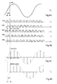
- FIGS. 2A to 2D illustrate the operation of the device of FIG. 1.
- FIG. 2A represents a periodic analog signal DLI which passes through 0 at an instant t0 'in advance of a duration ⁇ with respect to a reference instant t 0 .
- FIG. 2B shows the DLI2 signal. This DLI2 signal goes through zero at time t0 late by duration ⁇ 'by relative to the reference time t0.
- FIG. 2C represents the clock signal CK0 produced by the phase-locked loop 5.
- the reference instant t 0 is arbitrarily fixed by a rising edge of the clock signal CK0.
- Figure 2D represents two sequences of numerical values ANO1 and ANO2 sampled during rising edges successive of signal CK0.
- the control circuit 7 changes the delays ⁇ and ⁇ 'introduced by the delay lines between the DLO1 signals and DLO2 until the delay between the passage of the signal by 0 DLO1 and DLO2 signal either zero, or as low as possible, as allowed by the delay line pitch.
- the characteristics of a delay line, and in particular its no, can change considerably if the process of manufacturing changes. These variations in characteristics are not not desirable.
- an analog delay line is a delicate element the least modification of which must be carried out with the utmost care. It is an element called “not very portable” from one integrated circuit manufacturing technology to another.
- An object of the present invention is to provide a device for synchronizing a reference event of multiple analog signals, which can be realized in one CMOS technology.
- Another object of the present invention is to achieve such a synchronization device whose characteristics do not not vary depending on the manufacturing process.
- Another object of the present invention is to achieve such a synchronization device which is easily portable from one integrated circuit technology to another.
- Another object of the present invention is to achieve such a synchronization device having a pitch less than the nanosecond.
- the oscillator includes an even number of differential amplifiers balanced connected in an oscillating ring, an output an odd-rank amplifier providing the first signal clock, and the outputs of the even rank amplifiers providing said other clock signals.
- the analysis circuit includes a memory for storing the successive values of the register, and a microprocessor for analyze the successive values in order to determine the instants of zero crossing of the register output signal.
- a circuit comprising several devices for synchronization as described above, using a single phase locked loop and same signals clock.
- a control circuit for a laser disc player is provided as previously described, wherein each synchronization receives an analog signal from a head disc playback.
- the present invention exploits the presence of a converter analog / digital to achieve the goal. Instead of delay an analog signal using a delay line programmable analog, the signal is immediately converted analog to digital.
- the programmable delay is obtained thanks to the analog / digital converter which is clocked by a programmable phase clock signal.
- the converter output analog / digital is resynchronized on a clock general by a register receiving the output of the converter.
- FIG. 3 schematically represents a device for synchronization according to the present invention, comprising a converter analog / digital 3 which receives an analog signal periodic A and which provides a digital signal D to a register 9.
- a phase locked loop 5 includes an oscillator 11 providing a reference clock CKref.
- Locking loop phase 5 further includes a phase comparator 13 whose IC output controls an oscillator 15 via a low pass filter 17. The comparator 13 is connected to compare the phases of the reference clock CKref and a first clock signal CK0 produced by oscillator 15.
- the register 9 is clocked by the clock signal CK0.
- Oscillator 15 includes four differential amplifiers balanced 18 connected in an oscillating ring.
- a odd-rank amplifier output produces first clock signal CK0.
- Clock signals CK1 and CK2 are produced by the complementary outputs of a first amplifier of even rank of oscillator 15.
- the signals clock CK3 and CK4 are produced by complementary outputs the second even-numbered amplifier of oscillator 15.
- the filter 17 controls the supply current of the amplifiers and therefore the propagation time of the loop, corresponding at the oscillation period T.
- the four clock signals CK1 to CK4 are supplied to a multiplexer 19.
- the multiplexer 19, of which the output cadence the analog / digital converter 3, is controlled by an analysis circuit 21 which receives the REGO output from the register 9.
- FIGS. 4A to 4D illustrate the operation of the device in FIG. 3.
- FIG. 4A represents a periodic analog signal A which passes through 0 at an instant t 0 ', a duration A in advance with respect to a reference instant t 0 .
- FIG. 4B represents the clock signals CK0 to CK4.
- the instant t 0 is defined by a rising edge of the first clock signal CK0, the period T of which is here greater than the duration ⁇ .
- the clock signals CK1 and CK3 are phase shifted with respect to each other by a quarter of the period T and the signal CK1 is offset by one eighth of the period T with respect to the clock signal CK0. None of the clocks CK1 to CK4 are in phase with the clock signal CK0.
- FIG. 4C represents a succession of samples digital signals produced by the analog / digital converter 3, clocked by the successive rising edges of the clock signal supplied by multiplexer 19.
- Figure 4D shows a succession of samples numeric D produced by register 9, clocked by the edges successive amounts of the clock signal CK0. These samples are out of phase with the samples D of the difference of phase between the clock CKO and that supplied by the multiplexer.
- the analysis circuit 21 determines, as will be seen below, which of the clock signals CK1 to CK4 has the rising edge closest to the instant t 0 'of zero crossing of the signal A, and it controls the multiplexer 19 to select it. In the example shown, it selects the signal CK1, a rising edge of which occurs at time t 0 '. Thus clocked, the analog / digital converter 3 samples the input signal A at times t0 ', t0' + T, t0 '+ 2T, etc.
- register 9 receives the sampled value by converter 3, but it only takes it into account than at the next rising edge of the clock CK0, at time t0. Of same, the value sampled at time t0 '+ T by the converter 3 is taken into account at a time t0 + T by the register 9 And so on. It follows that the successive values taken by the REGO output of register 9 actually correspond to a sampling of the analog signal A by the signal clock CK0.
- the clock signal CK1 changes exactly at time t0 ', but we note that it can also change in a time interval equal to the smallest offset between two of the clock signals CK1 at CK4, here a quarter of the period T. Beyond this interval of time, signal CK1 would no longer be the signal whose edge amount is closest to time t0 ', and the analysis circuit 21 would select another clock signal. This introduces an imprecision equal to this time interval, which corresponds in step with this synchronization device.
- a device according to the present invention using an oscillator 15 with eight amplifiers differentials and a reference clock at 112 MHz allows make a synchronization device with a pitch of 1.16 nanoseconds. This step will be halved if we use sixteen differential amplifiers.
- the pitch of the synchronization device according to the present invention depends only on the frequency 1 / T of the oscillator 15 of the phase locked loop. This frequency does not depends only on the frequency of the reference clock and not on the device manufacturing process.
- the device according to the present invention is composed only elements achievable in CMOS technology and easy to transpose from one CMOS technology to another, which makes the particularly portable device.
- FIG. 5 represents an architecture of a circuit of control of a laser disc player comprising several devices synchronization according to the present invention. Likewise references designate the same elements as in FIG. 3.
- Such a circuit allows for example to integrate a circuit Tracking, conventionally carried out in BiCMOS technology, in a reader acquisition / control circuit, conventionally realized in CMOS technology.
- the tracking circuit receives of the disc read head of the analog centering signals which must be synchronized on the same clock and transmitted in digital form to a circuit microprocessor acquisition / enslavement.
- a read head 23 of a laser disc 24 provides four analog signals A1 to A4 to a preamplifier 25.
- Signals A1 to A4 are supplied by the preamplifier 25 with four analog / digital converters 3.
- Four multiplexers 19 respectively clock the four analog / digital converters 3 and each receives all four phase shifted clock signals CK1 to CK4 produced by a single phase locked loop 5.
- Digital signals produced by analog / digital converters, resynchronized by respective registers 9 are supplied to an analysis circuit unique 21.
- the registers 9 are clocked by a general clock CK0 supplied by loop 5.
- the analysis circuit 21 includes a memory 27 in which a table of numerical values is stored produced by the registers 9.
- the memory 27 is connected to a microprocessor 29, which provides a separate control signal to each of the multiplexers 19 according to an analysis of the board.
- the clock CK0 also rates the microprocessor 29 and memory 27.
- Microprocessor 29 uses the table to calculate by means of known algorithms the instants of passage through 0 of each of the signals A1 to A4. It compares the moments of passage by zero at the rising edges of the clock signals CK1 to CK4, and accordingly controls each multiplexer 19 to select one of these clock signals, so that the moments of passage by zero digital signals coincide with each other.
- the present invention is capable of various variants and modifications which will appear to the man of the job.
- we have described in relation to FIG. 3 a phase locked loop using only outputs even-range balanced differential amplifiers but it is possible to use the outputs of all amplifiers balanced differentials except for the one that produces the first clock signal CK0.
- Such a variant will make it possible to decrease the pitch of the synchronization device.
- the timing diagrams of FIGS. 4A to 4D illustrate a case where the converter 3 and register 9 are activated by edges clock signal amounts, but we can also, at the cost minor changes, use the falling edges of clock signals.
Abstract
Description
La présente invention concerne un dispositif de synchronisation de signaux analogiques. Dans une application particulière on utilise plusieurs de ces dispositifs associés à plusieurs signaux analogiques respectifs dans le but de faire coïncider des événements de référence des signaux.The present invention relates to a synchronization device analog signals. In an application particular we use several of these devices associated with several respective analog signals in order to make coincide signal reference events.
La figure 1 représente schématiquement un dispositif classique de synchronisation d'un événement de référence d'un signal analogique. Généralement, le dispositif est en outre prévu pour convertir le signal analogique synchronisé en un signal numérique.Figure 1 shows schematically a device classic synchronization of a reference event of a analog signal. Generally, the device is also provided to convert the synchronized analog signal into a signal digital.
Une ligne à retard programmable 1 reçoit un signal analogique
DLI1, et fournit un signal analogique retardé DLO1 à un
convertisseur analogique/numérique 3. Le convertisseur analogique/numérique
3 fournit des échantillons numériques D1 à la cadence
d'un signal d'horloge CKO produit par une boucle à verrouillage
de phase 5. Une ligne à retard programmable 2 reçoit un signal
analogique DLI2 et fournit un signal analogique retardé DLO2 à un
convertisseur analogique/numérique 4. Le convertisseur analogique/numérique
4 fournit des échantillons numériques D2 à la cadence
du signal d'horloge CKO. Les lignes à retard 1 et 2 sont respectivement
programmées par des signaux de commande COM(Δ) et
COM(Δ') produits par un circuit de commande 7 en fonction des
signaux DLI1 et DLI2.
Dans un exemple, l'événement de référence est un passage
par zéro du signal. Le circuit de commande 7 est alors prévu
pour régler les lignes à retard 1 et 2 de manière que le passage
par zéro du signal DLI1 soit synchronisé sur le passage par zéro
du signal DLI2.In an example, the reference event is a passage
by signal zero. The
Les figures 2A à 2D illustrent le fonctionnement du dispositif de la figure 1. La figure 2A représente un signal analogique périodique DLI qui passe par 0 en un instant t0' en avance d'une durée Δ par rapport à un instant de référence t0.FIGS. 2A to 2D illustrate the operation of the device of FIG. 1. FIG. 2A represents a periodic analog signal DLI which passes through 0 at an instant t0 'in advance of a duration Δ with respect to a reference instant t 0 .
La figure 2B représente le signal DLI2. Ce signal DLI2 passe par zéro à l'instant t0 en retard d'une durée Δ' par rapport à l'instant de référence t0.Figure 2B shows the DLI2 signal. This DLI2 signal goes through zero at time t0 late by duration Δ 'by relative to the reference time t0.
La figure 2C représente le signal d'horloge CK0 produit
par la boucle à verrouillage de phase 5. L'instant de référence
t0 est fixé arbitrairement par un front montant du signal d'horloge
CK0.FIG. 2C represents the clock signal CK0 produced by the phase-locked
La figure 2D représente deux suites de valeurs numériques ANO1 et ANO2 échantillonnées lors des fronts montants successifs du signal CK0.Figure 2D represents two sequences of numerical values ANO1 and ANO2 sampled during rising edges successive of signal CK0.
Le circuit de commande 7 fait évoluer les retards Δ et
Δ' introduits par les lignes à retard entre les signaux DLO1 et
DLO2 jusqu'à ce que le délai entre le passage par 0 du signal
DLO1 et du signal DLO2 soit nul, ou le plus faible possible,
selon ce que permet le pas de la ligne à retard.The
Bien qu'un circuit tel que celui de la figure 1 fonctionne de manière satisfaisante, il présente plusieurs inconvénients notables. En particulier, un circuit numérique comportant une ligne à retard analogique programmable ne peut être réalisé que dans une technologie BiCMOS, coûteuse.Although a circuit like the one in Figure 1 works satisfactorily, it has several disadvantages notable. In particular, a digital circuit comprising a programmable analog delay line cannot be realized than in expensive BiCMOS technology.
Les caractéristiques d'une ligne à retard, et en particulier son pas, peuvent changer considérablement si le processus de fabrication change. Ces variations de caractéristiques ne sont pas souhaitables. The characteristics of a delay line, and in particular its no, can change considerably if the process of manufacturing changes. These variations in characteristics are not not desirable.
D'autre part, une ligne à retard analogique est un élément délicat dont la moindre modification doit être réalisée avec le plus grand soin. C'est un élément dit "peu portable" d'une technologie de fabrication de circuit intégré à une autre.On the other hand, an analog delay line is a delicate element the least modification of which must be carried out with the utmost care. It is an element called "not very portable" from one integrated circuit manufacturing technology to another.
Enfin, les techniques courantes ne permettent pas d'obtenir des lignes à retard programmables ayant un pas inférieur à un ordre de la nanoseconde.Finally, current techniques do not allow obtain programmable delay lines with one step less than one nanosecond order.
Un objet de la présente invention est de réaliser un dispositif de synchronisation d'un événement de référence de plusieurs signaux analogiques, qui puisse être réalisé dans une technologie CMOS.An object of the present invention is to provide a device for synchronizing a reference event of multiple analog signals, which can be realized in one CMOS technology.
Un autre objet de la présente invention est de réaliser un tel dispositif de synchronisation dont les caractéristiques ne varient pas en fonction du processus de fabrication.Another object of the present invention is to achieve such a synchronization device whose characteristics do not not vary depending on the manufacturing process.
Un autre objet de la présente invention est de réaliser un tel dispositif de synchronisation qui soit facilement portable d'une technologie de circuit intégré à une autre.Another object of the present invention is to achieve such a synchronization device which is easily portable from one integrated circuit technology to another.
Un autre objet de la présente invention est de réaliser un tel dispositif de synchronisation ayant un pas inférieur à la nanoseconde.Another object of the present invention is to achieve such a synchronization device having a pitch less than the nanosecond.
Pour atteindre ces objets, ainsi que d'autres, la présente
invention prévoit un dispositif de synchronisation d'un
événement de référence d'un signal analogique, qui comprend :
Selon un mode de réalisation de la présente invention, l'oscillateur comprend un nombre pair d'amplificateurs différentiels équilibrés connectés en un anneau oscillant, une sortie d'un amplificateur de rang impair fournissant le premier signal d'horloge, et les sorties des amplificateurs de rang pair fournissant lesdits autres signaux d'horloge.According to an embodiment of the present invention, the oscillator includes an even number of differential amplifiers balanced connected in an oscillating ring, an output an odd-rank amplifier providing the first signal clock, and the outputs of the even rank amplifiers providing said other clock signals.
Selon un mode de réalisation de la présente invention, le circuit d'analyse comprend une mémoire pour stocker les valeurs successives du registre, et un microprocesseur pour analyser les valeurs successives afin de déterminer les instants de passage par zéro du signal de sortie du registre.According to an embodiment of the present invention, the analysis circuit includes a memory for storing the successive values of the register, and a microprocessor for analyze the successive values in order to determine the instants of zero crossing of the register output signal.
Selon un mode de réalisation de la présente invention, on prévoit un circuit comprenant plusieurs dispositifs de synchronisation tels que décrits précédemment, utilisant une unique boucle à verrouillage de phase et les mêmes signaux d'horloge.According to an embodiment of the present invention, a circuit is provided comprising several devices for synchronization as described above, using a single phase locked loop and same signals clock.
Selon un mode de réalisation de la présente invention, on prévoit un circuit de commande d'un lecteur de disque laser tel que décrit précédemment, dans lequel chaque dispositif de synchronisation reçoit un signal analogique provenant d'une tête de lecture du disque.According to an embodiment of the present invention, a control circuit for a laser disc player is provided as previously described, wherein each synchronization receives an analog signal from a head disc playback.
Ces objets, caractéristiques et avantages, ainsi que
d'autres de la présente invention seront exposés en détail dans
la description suivante de modes de réalisation particuliers
faite à titre non-limitatif en relation avec les figures jointes
parmi lesquelles :
La présente invention exploite la présence d'un convertisseur analogique/numérique pour atteindre le but visé. Au lieu de retarder un signal analogique au moyen d'une ligne à retard analogique programmable, on convertit immédiatement le signal analogique en numérique. Le retard programmable est obtenu grâce au convertisseur analogique/numérique que l'on cadence par un signal d'horloge de phase programmable. La sortie du convertisseur analogique/numérique est resynchronisée sur une horloge générale par un registre recevant la sortie du convertisseur.The present invention exploits the presence of a converter analog / digital to achieve the goal. Instead of delay an analog signal using a delay line programmable analog, the signal is immediately converted analog to digital. The programmable delay is obtained thanks to the analog / digital converter which is clocked by a programmable phase clock signal. The converter output analog / digital is resynchronized on a clock general by a register receiving the output of the converter.
La figure 3 représente schématiquement un dispositif de
synchronisation selon la présente invention, comportant un convertisseur
analogique/numérique 3 qui reçoit un signal analogique
périodique A et qui fournit un signal numérique D à un registre
9. Une boucle à verrouillage de phase 5 comprend un oscillateur
11 fournissant une horloge de référence CKref. La boucle à verrouillage
de phase 5 comprend en outre un comparateur de phase 13
dont la sortie IC commande un oscillateur 15 par l'intermédiaire
d'un filtre passe bas 17. Le comparateur 13 est connecté pour
comparer les phases de l'horloge de référence CKref et d'un
premier signal d'horloge CK0 produit par l'oscillateur 15. Le
registre 9 est cadencé par le signal d'horloge CK0.FIG. 3 schematically represents a device for
synchronization according to the present invention, comprising a converter
analog / digital 3 which receives an analog signal
periodic A and which provides a digital signal D to a
L'oscillateur 15 comprend quatre amplificateurs différentiels
équilibrés 18 connectés en un anneau oscillant. Une
sortie d'un amplificateur de rang impair produit le premier
signal d'horloge CK0. Des signaux d'horloge CK1 et CK2 sont
produits par les sorties complémentaires d'un premier amplificateur
de rang pair de l'oscillateur 15. De même, les signaux
d'horloge CK3 et CK4 sont produits par les sorties complémentaires
du second amplificateur de rang pair de l'oscillateur 15.
Le filtre 17 commande le courant d'alimentation des amplificateurs
et donc le temps de propagation de la boucle, correspondant
à la période d'oscillation T. Les quatre signaux d'horloge CK1 à
CK4 sont fournis à un multiplexeur 19. Le multiplexeur 19, dont
la sortie cadence le convertisseur analogique/numérique 3, est
commandé par un circuit d'analyse 21 qui reçoit la sortie REGO du
registre 9.
Les figures 4A à 4D illustrent le fonctionnement du dispositif de la figure 3. La figure 4A représente un signal analogique périodique A qui passe par 0 à un instant t0', une durée A en avance par rapport à un instant de référence t0.FIGS. 4A to 4D illustrate the operation of the device in FIG. 3. FIG. 4A represents a periodic analog signal A which passes through 0 at an instant t 0 ', a duration A in advance with respect to a reference instant t 0 .
La figure 4B représente les signaux d'horloge CK0 à CK4. L'instant t0 est défini par un front montant du premier signal d'horloge CK0, dont la période T est ici supérieure à la durée Δ. Les signaux d'horloge CK1 et CK3 sont déphasés l'un par rapport à l'autre d'un quart de la période T et le signal CK1 est décalé d'un huitième de la période T par rapport au signal d'horloge CK0. Aucune des horloges CK1 à CK4 n'est en phase avec le signal d'horloge CK0.FIG. 4B represents the clock signals CK0 to CK4. The instant t 0 is defined by a rising edge of the first clock signal CK0, the period T of which is here greater than the duration Δ. The clock signals CK1 and CK3 are phase shifted with respect to each other by a quarter of the period T and the signal CK1 is offset by one eighth of the period T with respect to the clock signal CK0. None of the clocks CK1 to CK4 are in phase with the clock signal CK0.
La figure 4C représente une succession d'échantillons
numériques D produite par le convertisseur analogique/numérique
3, cadencé par les fronts montants successifs du signal d'horloge
fourni par le multiplexeur 19.FIG. 4C represents a succession of samples
digital signals produced by the analog /
La figure 4D représente une succession d'échantillons
numériques D produite par le registre 9, cadencé par les fronts
montants successifs du signal d'horloge CK0. Ces échantillons
sont déphasés par rapport aux échantillons D de la différence de
phase entre l'horloge CKO et celle qui est fournie par le multiplexeur.Figure 4D shows a succession of samples
numeric D produced by
Le circuit d'analyse 21 détermine, comme on le verra
par la suite, lequel des signaux d'horloge CK1 à CK4 présente le
front montant le plus proche de l'instant t0' de passage par zéro
du signal A, et il commande le multiplexeur 19 pour le sélectionner.
Dans l'exemple représenté, il sélectionne le signal CK1 dont
un front montant se produit à l'instant t0'. Ainsi cadencé, le
convertisseur analogique/numérique 3 échantillonne le signal
d'entrée A aux instants t0', t0'+T, t0'+2T, etc. The
A l'instant t0', le registre 9 reçoit la valeur échantillonnée
par le convertisseur 3, mais il ne la prend en compte
qu'au front montant suivant de l'horloge CK0, à l'instant t0. De
même, la valeur échantillonnée à l'instant t0'+T par le convertisseur
3 est prise en compte à un instant t0+T par le registre 9
et ainsi de suite. Il en découle que les valeurs successives
prises par la sortie REGO du registre 9 correspondent effectivement
à un échantillonnage du signal analogique A par le signal
d'horloge CK0.At time t0 ', register 9 receives the sampled value
by
Par souci de clarté, dans l'exemple représenté, le
signal d'horloge CK1 change exactement à l'instant t0', mais on
notera qu'il peut également changer dans un intervalle de temps
égal au plus petit décalage entre deux des signaux d'horloge CK1
à CK4, ici un quart de la période T. Au delà de cet intervalle de
temps, le signal CK1 ne serait plus le signal dont le front
montant est le plus proche de l'instant t0', et le circuit d'analyse
21 sélectionnerait un autre signal d'horloge. Ceci introduit
une imprécision égale à cet intervalle de temps, qui correspond
au pas du présent dispositif de synchronisation.For the sake of clarity, in the example shown, the
clock signal CK1 changes exactly at time t0 ', but we
note that it can also change in a time interval
equal to the smallest offset between two of the clock signals CK1
at CK4, here a quarter of the period T. Beyond this interval of
time, signal CK1 would no longer be the signal whose edge
amount is closest to time t0 ', and the
Si l'on souhaite synchroniser un signal analogique de
manière plus fine, on peut diminuer ce pas en augmentant la
fréquence du signal d'horloge de référence CKref ou bien prévoir
un oscillateur 15 comportant un plus grand nombre d'amplificateurs
différentiels équilibrés.If you want to synchronize an analog signal from
more finely, we can decrease this step by increasing the
frequency of the reference clock signal CKref or else provide
an
A titre d'exemple, un dispositif selon la présente
invention utilisant un l'oscillateur 15 à huit amplificateurs
différentiels et une horloge de référence à 112 MHz, permet de
réaliser un dispositif de synchronisation ayant un pas de 1,16
nanosecondes. Ce pas sera divisé par deux si on utilise seize
amplificateurs différentiels.By way of example, a device according to the present
invention using an
Si l'on veut retarder le signal A d'une durée Δ+nT, où n est un entier quelconque, il suffit de retarder le signal A de Δ comme décrit ci-dessus, puis d'ajouter en sortie du registre 9 une ligne à retard numérique de n étages cadencée à la période T. If we want to delay signal A by a duration Δ + nT, where n is any integer, just delay signal A by Δ as described above, then add at the output of register 9 a digital delay line of n stages clocked in period T.
On remarquera que le pas du dispositif de synchronisation
selon la présente invention, égal à T/4 dans l'exemple
présenté, ne dépend que de la fréquence 1/T de l'oscillateur 15
de la boucle à verrouillage de phase. Or cette fréquence ne
dépend que de la fréquence de l'horloge de référence et non du
processus de fabrication du dispositif.Note that the pitch of the synchronization device
according to the present invention, equal to T / 4 in the example
presented, depends only on the
Le dispositif selon la présente invention est composé uniquement d'éléments réalisables en technologie CMOS et faciles à transposer d'une technologie CMOS à une autre, ce qui rend le dispositif particulièrement portable.The device according to the present invention is composed only elements achievable in CMOS technology and easy to transpose from one CMOS technology to another, which makes the particularly portable device.
La figure 5 représente une architecture d'un circuit de commande d'un lecteur de disque laser comprenant plusieurs dispositifs de synchronisation selon la présente invention. De mêmes références désignent des mêmes éléments qu'à la figure 3.FIG. 5 represents an architecture of a circuit of control of a laser disc player comprising several devices synchronization according to the present invention. Likewise references designate the same elements as in FIG. 3.
Un tel circuit permet par exemple d'intégrer un circuit de suivi (Tracking), classiquement réalisé en technologie BiCMOS, dans un circuit d'acquisition/asservissement du lecteur, classiquement réalisé en technologie CMOS. Le circuit de suivi reçoit de la tête de lecture du disque des signaux analogiques de centrage qui doivent être synchronisés sur une même horloge et transmis sous forme numérique à un microprocesseur du circuit d'acquisition/asservissement.Such a circuit allows for example to integrate a circuit Tracking, conventionally carried out in BiCMOS technology, in a reader acquisition / control circuit, conventionally realized in CMOS technology. The tracking circuit receives of the disc read head of the analog centering signals which must be synchronized on the same clock and transmitted in digital form to a circuit microprocessor acquisition / enslavement.
Dans l'exemple illustré, une tête 23 de lecture d'un
disque laser 24 fournit quatre signaux analogiques A1 à A4 à un
préamplificateur 25. Les signaux A1 à A4 sont fournis par le
préamplificateur 25 à quatre convertisseurs analogique/numérique
3. Quatre multiplexeurs 19 cadencent respectivement les quatre
convertisseurs analogique/numérique 3 et chacun reçoit les quatre
signaux d'horloge déphasés CK1 à CK4 produits par une unique
boucle à verrouillage de phase 5. Les signaux numériques produits
par les convertisseurs analogique/numérique, resynchronisés par
des registres respectifs 9, sont fournis à un circuit d'analyse
unique 21. Les registres 9 sont cadencés par une horloge générale
CK0 fournie par la boucle 5. Le circuit d'analyse 21 comprend une
mémoire 27 dans laquelle est stocké un tableau des valeurs numériques
produites par les registres 9. La mémoire 27 est reliée à
un microprocesseur 29, qui fournit un signal de commande distinct
à chacun des multiplexeurs 19 en fonction d'une analyse du
tableau. L'horloge CK0 cadence également le microprocesseur 29 et
la mémoire 27.In the example illustrated, a
Le microprocesseur 29 utilise le tableau pour calculer
au moyen d'algorithmes connus les instants de passage par 0 de
chacun des signaux A1 à A4. Il compare les instants de passage
par zéro aux fronts montants des signaux d'horloge CK1 à CK4, et
commande en conséquence chaque multiplexeur 19 pour sélectionner
l'un de ces signaux d'horloge, afin que les instants de passage
par zéro des signaux numériques coïncident les uns avec les
autres.
Bien entendu, la présente invention est susceptible de
diverses variantes et modifications qui apparaítront à l'homme du
métier. Par exemple, on a décrit en relation avec la figure 3 une
boucle à verrouillage de phase utilisant uniquement les sorties
des amplificateurs différentiels équilibrés de rang pair, mais il
est possible d'utiliser les sorties de tous les amplificateurs
différentiels équilibrés à l'exception de celle qui produit le
premier signal d'horloge CK0. Une telle variante permettra de
diminuer le pas du dispositif de synchronisation. D'autre part,
les chronogrammes des figures 4A à 4D illustrent un cas où le
convertisseur 3 et le registre 9 sont activés par des fronts
montants des signaux d'horloge, mais on pourra également, au prix
de modifications mineures, utiliser les fronts descendants des
signaux d'horloge.Of course, the present invention is capable of
various variants and modifications which will appear to the man of the
job. For example, we have described in relation to FIG. 3 a
phase locked loop using only outputs
even-range balanced differential amplifiers but it
is possible to use the outputs of all amplifiers
balanced differentials except for the one that produces the
first clock signal CK0. Such a variant will make it possible to
decrease the pitch of the synchronization device. On the other hand,
the timing diagrams of FIGS. 4A to 4D illustrate a case where the
L'emploi d'amplificateurs opérationnels dans l'anneau oscillant décrit précédemment permet de diminuer la gigue des signaux produits par l'oscillateur en rejetant le bruit de mode commun. Cependant, on notera qu'on pourra également utiliser un autre type d'anneau oscillant pour l'oscillateur, utilisant par exemple un nombre impair d'inverseurs.The use of operational amplifiers in the ring oscillating described previously makes it possible to decrease the jitter of signals produced by the oscillator while rejecting the mode noise common. However, note that we can also use a other type of oscillating ring for the oscillator, using by example an odd number of inverters.
Enfin, la description précédente ne concerne que la synchronisation du passage par zéro d'un signal d'entrée, mais la présente invention est également applicable à la synchronisation d'un autre événement, comme le passage du signal d'entrée par une valeur maximale ou minimale.Finally, the previous description only concerns the synchronization of the zero crossing of an input signal, but the present invention is also applicable to synchronization another event, such as the passing of the input signal through a maximum or minimum value.
Claims (5)
Applications Claiming Priority (2)
| Application Number | Priority Date | Filing Date | Title |
|---|---|---|---|
| FR9910089A FR2797121B1 (en) | 1999-07-30 | 1999-07-30 | DEVICE FOR SYNCHRONIZING A REFERENCE EVENT OF AN ANALOG SIGNAL ON A CLOCK |
| FR9910089 | 1999-07-30 |
Publications (2)
| Publication Number | Publication Date |
|---|---|
| EP1073204A1 true EP1073204A1 (en) | 2001-01-31 |
| EP1073204B1 EP1073204B1 (en) | 2004-06-16 |
Family
ID=9548852
Family Applications (1)
| Application Number | Title | Priority Date | Filing Date |
|---|---|---|---|
| EP00410085A Expired - Lifetime EP1073204B1 (en) | 1999-07-30 | 2000-07-28 | Arrangement for synchronizing a reference event of an analog signal to a clock signal |
Country Status (4)
| Country | Link |
|---|---|
| US (1) | US6304113B1 (en) |
| EP (1) | EP1073204B1 (en) |
| DE (1) | DE60011524T2 (en) |
| FR (1) | FR2797121B1 (en) |
Cited By (1)
| Publication number | Priority date | Publication date | Assignee | Title |
|---|---|---|---|---|
| FR2820521A1 (en) * | 2001-02-02 | 2002-08-09 | St Microelectronics Sa | METHOD AND DEVICE FOR GENERATING A SYNCHRONIZATION VARIABLE, INTEGRATED CIRCUIT AND DIGITAL DISK DRIVE |
Families Citing this family (6)
| Publication number | Priority date | Publication date | Assignee | Title |
|---|---|---|---|---|
| US7424636B1 (en) * | 2000-08-10 | 2008-09-09 | Alcatel Lucent | Method and apparatus for controlling a clock signal of a line card circuit |
| US7427815B1 (en) * | 2003-11-14 | 2008-09-23 | General Electric Company | Method, memory media and apparatus for detection of grid disconnect |
| KR100689832B1 (en) * | 2005-06-21 | 2007-03-08 | 삼성전자주식회사 | Phase locked loop and method |
| US8112233B2 (en) * | 2005-07-21 | 2012-02-07 | The Invention Science Fund I, Llc | Selective resonance of chemical structures |
| KR100714892B1 (en) * | 2005-10-26 | 2007-05-04 | 삼성전자주식회사 | Clock signal generator and phase and delay locked loop comprising the same |
| US8004335B2 (en) * | 2008-02-11 | 2011-08-23 | International Business Machines Corporation | Phase interpolator system and associated methods |
Citations (4)
| Publication number | Priority date | Publication date | Assignee | Title |
|---|---|---|---|---|
| EP0680170A1 (en) * | 1994-04-29 | 1995-11-02 | STMicroelectronics S.A. | Circuit for the transmission of a line-coded signal on a telephone line with a frequency synchroniser |
| US5553104A (en) * | 1993-06-29 | 1996-09-03 | Hitachi, Ltd. | Information recording/reproducing apparatus having a clock timing extraction circuit for extracting a clock signal from an input data signal |
| US5646968A (en) * | 1995-11-17 | 1997-07-08 | Analog Devices, Inc. | Dynamic phase selector phase locked loop circuit |
| GB2310772A (en) * | 1996-02-29 | 1997-09-03 | Sony Corp | Variable frequency ring oscillator and phase locked loop using such oscillator |
Family Cites Families (2)
| Publication number | Priority date | Publication date | Assignee | Title |
|---|---|---|---|---|
| US5838738A (en) * | 1996-07-29 | 1998-11-17 | Cirrus Logic, Inc. | Coding to improve timing recovery in a sampled amplitude read channel |
| US5978425A (en) * | 1997-05-23 | 1999-11-02 | Hitachi Micro Systems, Inc. | Hybrid phase-locked loop employing analog and digital loop filters |
-
1999
- 1999-07-30 FR FR9910089A patent/FR2797121B1/en not_active Expired - Fee Related
-
2000
- 2000-07-28 EP EP00410085A patent/EP1073204B1/en not_active Expired - Lifetime
- 2000-07-28 US US09/627,272 patent/US6304113B1/en not_active Expired - Fee Related
- 2000-07-28 DE DE60011524T patent/DE60011524T2/en not_active Expired - Fee Related
Patent Citations (4)
| Publication number | Priority date | Publication date | Assignee | Title |
|---|---|---|---|---|
| US5553104A (en) * | 1993-06-29 | 1996-09-03 | Hitachi, Ltd. | Information recording/reproducing apparatus having a clock timing extraction circuit for extracting a clock signal from an input data signal |
| EP0680170A1 (en) * | 1994-04-29 | 1995-11-02 | STMicroelectronics S.A. | Circuit for the transmission of a line-coded signal on a telephone line with a frequency synchroniser |
| US5646968A (en) * | 1995-11-17 | 1997-07-08 | Analog Devices, Inc. | Dynamic phase selector phase locked loop circuit |
| GB2310772A (en) * | 1996-02-29 | 1997-09-03 | Sony Corp | Variable frequency ring oscillator and phase locked loop using such oscillator |
Non-Patent Citations (1)
| Title |
|---|
| BATRUNI R ET AL: "MIXED DIGITAL/ANALOG SIGNAL PROCESSING FOR A SINGLE-CHIP 2B1Q U-INTERFACE TRANSCEIVER", IEEE JOURNAL OF SOLID-STATE CIRCUITS,US,IEEE INC. NEW YORK, vol. 25, no. 6, 1 December 1990 (1990-12-01), pages 1414 - 1425, XP000176570, ISSN: 0018-9200 * |
Cited By (3)
| Publication number | Priority date | Publication date | Assignee | Title |
|---|---|---|---|---|
| FR2820521A1 (en) * | 2001-02-02 | 2002-08-09 | St Microelectronics Sa | METHOD AND DEVICE FOR GENERATING A SYNCHRONIZATION VARIABLE, INTEGRATED CIRCUIT AND DIGITAL DISK DRIVE |
| WO2002063444A1 (en) * | 2001-02-02 | 2002-08-15 | Stmicroelectronics Sa | Method and device for generating a synchronisation variable and the corresponding integrated circuit and digital disc drive |
| US7219297B2 (en) | 2001-02-02 | 2007-05-15 | Stmicroelectronics Sa | Method and device for generating a synchronization variable and the corresponding integrated circuit and digital disc drive |
Also Published As
| Publication number | Publication date |
|---|---|
| FR2797121B1 (en) | 2001-10-12 |
| DE60011524D1 (en) | 2004-07-22 |
| FR2797121A1 (en) | 2001-02-02 |
| US6304113B1 (en) | 2001-10-16 |
| EP1073204B1 (en) | 2004-06-16 |
| DE60011524T2 (en) | 2005-08-18 |
Similar Documents
| Publication | Publication Date | Title |
|---|---|---|
| EP0641083A1 (en) | Frequency synthesizer | |
| FR2882871A1 (en) | LOW VOLTAGE CONTROLLED VOLTAGE CONTROL OSCILLATOR AND ASSOCIATED PHASE LOOP | |
| EP0595734B1 (en) | Multiplexer receiving at its input a plurality of identical signals differing only in phase | |
| EP0142440A2 (en) | Generating device for a frequency being a fraction of a reference frequency | |
| EP1073204B1 (en) | Arrangement for synchronizing a reference event of an analog signal to a clock signal | |
| FR2728118A1 (en) | PHASE COMPARATOR BETWEEN A DIGITAL SIGNAL AND A CLOCK SIGNAL, AND CORRESPONDING PHASE LOCKING BUCKLE | |
| FR2908948A1 (en) | DIGITAL PHASE LOCK BUCKLE | |
| FR2851095A1 (en) | Phase lock loop for frequency synthesizer, has oscillator to produce signals with phase difference based on control voltage, and control unit to control multiplexer to provide predetermined fractions of signal | |
| EP0071506A1 (en) | Digital method and device for the phase error correction of a sampled signal and its application to the correction of television signals | |
| EP0753941A1 (en) | Frequency synthesizer | |
| EP1424774A1 (en) | Random number generator | |
| EP0715415B1 (en) | Device for serialising high data rate binary data | |
| FR2585169A1 (en) | PERFECTED CLOCK RECOVERY SYSTEM FOR DIGITAL MAGNETIC REPRODUCTION DEVICE | |
| EP0647018A1 (en) | Digital phase comparator | |
| EP0197801A2 (en) | Method and device for quickly setting the phase of a clock signal at a predetermined value | |
| FR2635623A1 (en) | SYNCHRONIZATION DEVICE ON DIGITAL DATA PACKETS AND READER COMPRISING SAME | |
| EP1606880B1 (en) | Frequency divider with variable division rate | |
| EP0689315B1 (en) | Phase comparator | |
| FR2714240A1 (en) | Phase difference compensation system for digital data frames | |
| EP0729082B1 (en) | Very precise chrono-measurement of an event | |
| FR2710208A1 (en) | Digital first order integrator and filter. | |
| EP0869619A1 (en) | Integrated circuit comprising a phase controlled loop | |
| JP2660442B2 (en) | Digital reference clock generation circuit | |
| FR3133458A1 (en) | Time sequence generation circuit | |
| EP3716523A1 (en) | Method for synchronising digital data sent in series |
Legal Events
| Date | Code | Title | Description |
|---|---|---|---|
| PUAI | Public reference made under article 153(3) epc to a published international application that has entered the european phase |
Free format text: ORIGINAL CODE: 0009012 |
|
| AK | Designated contracting states |
Kind code of ref document: A1 Designated state(s): DE FR GB IT |
|
| AX | Request for extension of the european patent |
Free format text: AL;LT;LV;MK;RO;SI |
|
| 17P | Request for examination filed |
Effective date: 20010716 |
|
| AKX | Designation fees paid |
Free format text: DE FR GB IT |
|
| RAP1 | Party data changed (applicant data changed or rights of an application transferred) |
Owner name: STMICROELECTRONICS S.A. |
|
| GRAP | Despatch of communication of intention to grant a patent |
Free format text: ORIGINAL CODE: EPIDOSNIGR1 |
|
| GRAS | Grant fee paid |
Free format text: ORIGINAL CODE: EPIDOSNIGR3 |
|
| GRAA | (expected) grant |
Free format text: ORIGINAL CODE: 0009210 |
|
| AK | Designated contracting states |
Kind code of ref document: B1 Designated state(s): DE FR GB IT |
|
| PG25 | Lapsed in a contracting state [announced via postgrant information from national office to epo] |
Ref country code: IT Free format text: LAPSE BECAUSE OF FAILURE TO SUBMIT A TRANSLATION OF THE DESCRIPTION OR TO PAY THE FEE WITHIN THE PRESCRIBED TIME-LIMIT;WARNING: LAPSES OF ITALIAN PATENTS WITH EFFECTIVE DATE BEFORE 2007 MAY HAVE OCCURRED AT ANY TIME BEFORE 2007. THE CORRECT EFFECTIVE DATE MAY BE DIFFERENT FROM THE ONE RECORDED. Effective date: 20040616 |
|
| REG | Reference to a national code |
Ref country code: GB Ref legal event code: FG4D Free format text: NOT ENGLISH |
|
| GBT | Gb: translation of ep patent filed (gb section 77(6)(a)/1977) |
Effective date: 20040616 |
|
| REF | Corresponds to: |
Ref document number: 60011524 Country of ref document: DE Date of ref document: 20040722 Kind code of ref document: P |
|
| PLBE | No opposition filed within time limit |
Free format text: ORIGINAL CODE: 0009261 |
|
| STAA | Information on the status of an ep patent application or granted ep patent |
Free format text: STATUS: NO OPPOSITION FILED WITHIN TIME LIMIT |
|
| 26N | No opposition filed |
Effective date: 20050317 |
|
| PGFP | Annual fee paid to national office [announced via postgrant information from national office to epo] |
Ref country code: FR Payment date: 20060719 Year of fee payment: 7 |
|
| PGFP | Annual fee paid to national office [announced via postgrant information from national office to epo] |
Ref country code: DE Payment date: 20060720 Year of fee payment: 7 |
|
| PGFP | Annual fee paid to national office [announced via postgrant information from national office to epo] |
Ref country code: GB Payment date: 20060726 Year of fee payment: 7 |
|
| GBPC | Gb: european patent ceased through non-payment of renewal fee |
Effective date: 20070728 |
|
| PG25 | Lapsed in a contracting state [announced via postgrant information from national office to epo] |
Ref country code: DE Free format text: LAPSE BECAUSE OF NON-PAYMENT OF DUE FEES Effective date: 20080201 |
|
| PG25 | Lapsed in a contracting state [announced via postgrant information from national office to epo] |
Ref country code: GB Free format text: LAPSE BECAUSE OF NON-PAYMENT OF DUE FEES Effective date: 20070728 |
|
| REG | Reference to a national code |
Ref country code: FR Ref legal event code: ST Effective date: 20080331 |
|
| PG25 | Lapsed in a contracting state [announced via postgrant information from national office to epo] |
Ref country code: FR Free format text: LAPSE BECAUSE OF NON-PAYMENT OF DUE FEES Effective date: 20070731 |