EP1073196A2 - Signal notching system for limiting signal peaks - Google Patents
Signal notching system for limiting signal peaks Download PDFInfo
- Publication number
- EP1073196A2 EP1073196A2 EP00306070A EP00306070A EP1073196A2 EP 1073196 A2 EP1073196 A2 EP 1073196A2 EP 00306070 A EP00306070 A EP 00306070A EP 00306070 A EP00306070 A EP 00306070A EP 1073196 A2 EP1073196 A2 EP 1073196A2
- Authority
- EP
- European Patent Office
- Prior art keywords
- sample
- peak
- signal
- threshold
- notching
- Prior art date
- Legal status (The legal status is an assumption and is not a legal conclusion. Google has not performed a legal analysis and makes no representation as to the accuracy of the status listed.)
- Granted
Links
- 238000000034 method Methods 0.000 claims description 26
- 238000001914 filtration Methods 0.000 claims description 10
- 238000004891 communication Methods 0.000 claims description 4
- 238000001514 detection method Methods 0.000 claims description 4
- 238000012545 processing Methods 0.000 claims description 3
- 230000000875 corresponding effect Effects 0.000 description 7
- 238000005070 sampling Methods 0.000 description 7
- 230000003595 spectral effect Effects 0.000 description 7
- 238000001228 spectrum Methods 0.000 description 5
- 230000007423 decrease Effects 0.000 description 4
- 230000008569 process Effects 0.000 description 4
- 101000910089 Candida albicans (strain SC5314 / ATCC MYA-2876) Candidapepsin-5 Proteins 0.000 description 3
- 230000008901 benefit Effects 0.000 description 3
- 238000012546 transfer Methods 0.000 description 3
- 230000001934 delay Effects 0.000 description 2
- 230000004044 response Effects 0.000 description 2
- 230000004075 alteration Effects 0.000 description 1
- 230000002238 attenuated effect Effects 0.000 description 1
- 230000001413 cellular effect Effects 0.000 description 1
- 230000001419 dependent effect Effects 0.000 description 1
- 238000010586 diagram Methods 0.000 description 1
- 238000012986 modification Methods 0.000 description 1
- 230000004048 modification Effects 0.000 description 1
- 230000009467 reduction Effects 0.000 description 1
- 238000004088 simulation Methods 0.000 description 1
Images


Classifications
-
- H—ELECTRICITY
- H03—ELECTRONIC CIRCUITRY
- H03G—CONTROL OF AMPLIFICATION
- H03G11/00—Limiting amplitude; Limiting rate of change of amplitude
-
- H—ELECTRICITY
- H03—ELECTRONIC CIRCUITRY
- H03F—AMPLIFIERS
- H03F1/00—Details of amplifiers with only discharge tubes, only semiconductor devices or only unspecified devices as amplifying elements
- H03F1/32—Modifications of amplifiers to reduce non-linear distortion
- H03F1/3241—Modifications of amplifiers to reduce non-linear distortion using predistortion circuits
-
- H—ELECTRICITY
- H03—ELECTRONIC CIRCUITRY
- H03F—AMPLIFIERS
- H03F2201/00—Indexing scheme relating to details of amplifiers with only discharge tubes, only semiconductor devices or only unspecified devices as amplifying elements covered by H03F1/00
- H03F2201/32—Indexing scheme relating to modifications of amplifiers to reduce non-linear distortion
- H03F2201/3236—A generated signal, e.g. a pulse or an inverted synchronous signal, being added to avoid certain conditions, e.g. clipping
-
- H—ELECTRICITY
- H04—ELECTRIC COMMUNICATION TECHNIQUE
- H04B—TRANSMISSION
- H04B1/00—Details of transmission systems, not covered by a single one of groups H04B3/00 - H04B13/00; Details of transmission systems not characterised by the medium used for transmission
- H04B1/02—Transmitters
- H04B1/04—Circuits
- H04B1/0475—Circuits with means for limiting noise, interference or distortion
Definitions
- This invention relates to communications systems, and more particularly to a system for reducing the peaks of a signal to be amplified.
- An ideal power amplifier amplifies an input signal of a given bandwidth with no waveshape alteration.
- the ideal power amplifier is therefore characterized as having a transfer function (input signal vs. output signal) which is linear with no transfer function discontinuities.
- a power amplifier has a transfer function with nonlinear and "linear" regions. Whether the power amplifier is operating in a linear or nonlinear region depends on the amplitude of the input signal. For the power amplifier to achieve as near to linear operation as possible, the power amplifier is designed to operate within its linear region given the range of possible input signal amplitudes. If the input signal has an amplitude which causes the power amplifier to operate outside the linear region, the power amplifier introduces nonlinear components or distortion to the signal.
- an amplifier When the input signal peak amplitude causes the amplifier to saturate (no appreciable increase in output amplitude with an increase in input amplitude) or to shut-off (no appreciable decrease in output amplitude with a decrease in input amplitude), the amplifier is being overdriven, and the output signal is clipped or distorted.
- an amplifier is characterized as having a clipping threshold, and input signals having amplitudes beyond the clipping threshold are clipped at the amplifier output.
- the clipping or nonlinear distortion of the input signal causes power to be generated in adjacent channels or frequencies to corrupt or interfere with signals in the adjacent channels or frequencies, commonly referred to as spectral regrowth or adjacent channel power (ACP).
- ACP adjacent channel power
- the generation of adjacent channel power is of particular concern in wireless communications systems where signals being amplified are in adjacent channels or frequency bands.
- the peak to average power ratio (PAR) for a single loaded code division multiple access (CDMA) 1.25 MHz carrier is about 11.3 dB measured at 10 -4 peaking probability (indicating a 1/10,000 chance that a peak exceeds a threshold value for example of 8.5 dB above the average power).
- a high cost, low efficiency power amplifier is operated at an average power level far below its saturation point to avoid distorting the peaks and generating ACP.
- methods have been proposed for reducing the PAR of the signal without generating significant ACP or spectral regrowth which occurs when power from the signal appears at different frequency bands.
- a straight forward method for PAR reduction involves hardlimiting or hard clipping the signal peaks to a certain hardlimiting threshold to lower the PAR.
- a hard clipped signal however, has abrupt edges and the short time duration of the clipped edges generates significant adjacent channel power and spectral regrowth in the frequency domain.
- a filter can be used to remove the ACP and the spectral regrowth.
- the filter can be implemented at baseband or intermediate frequency (IF) where sharp filters are readily available either in digital or analog form.
- IF intermediate frequency
- a digital implementation at baseband is favored because of its flexibility and low cost. It has been found, however, that after filtering the clipped signal, the signal peaks grow back.
- the peaks could be detected using the desired threshold, then the peaks above the detection threshold are hardlimited to a new limit lower than the detection threshold.
- the peaks grow back alter the cleanup filtering, they would still be below the targeted value.
- this method is as easy to implement as the simple hardlimiting.
- the peaks that are slightly above the threshold only needs to be clipped lightly and their growth after cleanup filtering is also small. By clipping all these peaks to the new limit, the peaks that are slightly above the threshold can be over-clipped.
- U.S. Patent No. 5,287,387 discloses a window clipping method for reducing the peak to average power ratio of an input signal.
- an attenuating window is centered about a local maximum of a signal peak above a threshold, and the attenuating window is multiplied with the input signal to generate an attenuated signal.
- the attenuating window is comprised of multiple sample weights which are valued at less than one. The multiple weights of the attenuating window are multiplied with corresponding peak samples of the input signal to reduce the peak of the input signal to below a threshold.
- multiplying the signals in the time domain is equivalent to convolving the spectrum of the input signal with the window spectrum in the frequency domain, thereby altering the spectrum of the window clipped signal.
- the window clipping process fails to adequately address the problems of the hard clipping processes.
- the present invention reduces signal peaks by notching the peak of a signal above a threshold to produce a notched signal.
- the notched signal is then filtered to produce a resulting signal with a reduced peak amplitude.
- the peak notching system first locates a peak sample that is beyond a threshold, such as a sample representing a positive peak sample of a peak above the threshold. Once a peak sample is located, the peak notching system adjusts the peak sample by an amount which is a function of the amount that the peak sample is beyond the threshold, effectively creating a notched signal with a one sample notch at the peak.
- the peak notching system filters the notched signal to fill in the notch to produce a signal with a reduced peak.
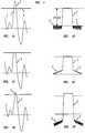
- FIG. 1A shows an example baseband in-phase waveform 2, such as a 1.25 MHz CDMA carrier, in the time domain with a peak 3 above a threshold 4, and FIG. 1B shows the corresponding spectral representation with the ACP 5 being 45 dB below the signal 2.
- FIG. 1C illustrates how the hard limiting procedure clips the signal 2
- FIG. 1D shows the corresponding effect or increase in the ACP 5 on the signal spectrum for a single carrier IS-95 system.
- the peaks 7 grow back as shown in FIG. 1E.
- the threshold has to be set to about 1.5 dB below the target, causing a large number of peaks that are below the targeted maximum to be clipped.
- FIG. 2A shows a signal 10 to be amplified, and the signal 10 is shown in the time domain with a peak 12 having an amplitude (for example voltage) above a threshold 14.
- FIG. 2B shows the signal 10 in the frequency domain, such as a 1.25 MHz carrier which is 45 dB above adjacent channel power 16.
- the signal 10 is shown as an analog signal, but it should be understood that the peak notching system can sample the signal 10 to obtain signal samples, shown as lines within the envelope of the signal 10, which are used to represent the signal 10.
- the peak notching system locates a peak sample 18 representing the maximum of the peak 12 above the threshold 14.
- the peak notching system in this embodiment adjusts the amplitude (for example, the voltage) of the peak sample 18 by an amount which is a function of the amount that the peak sample exceeds the threshold, effectively creating a notched signal 20 in the time domain with a one-sample notch 22 at the top of the peak 12 as shown in FIG. 2C.
- the adjacent channel power 16 increases due to the notching of the signal 10 to produce the notched signal 20.
- the notching of the signal 10 reduces the in-band power or energy of the signal and increases the out-of-band power or energy.
- the notched signal 20 is filtered to fill in the notch and produce a signal 24 shown with a reduced PAR as shown in FIG. 2E and with reduced adjacent channel power as shown in FIG. 2F.
- the filter reduces the power or energy outside the band and passes or retains the in-band power or energy.
- the out-of band power produced by the notching is removed, and the resulting signal has an amplitude adjusted by an amount depending on the amount that the original peak sample is beyond the threshold.
- the amount by which the peak sample is adjusted is a function of the amount that the peak sample exceeds the threshold.
- the amount that the peak sample is reduced can be determined as a function of the amount that the peak sample exceeds the threshold and a scaling factor.
- the scaling factor is dependent on the oversampling ratio.
- the sampling rate is the rate at which the signal is sampled. If a waveform is sampled at twice the highest frequency sine wave component, then the original signal can be reconstructed from the sample points. As such, the minimum sampling rate would be 2 times the frequency of the signal.
- the oversampling ratio can be determined by the sampling rate + minimum sampling rate required to reconstruct the signal or 2.
- a sampling rate of 8 times the frequency of the signal is performed which provides an oversampling ratio of 4.
- the scaling factor is approximately 4. If a greater oversampling ratio is used, the scaling factor would increase, and if the oversampling ratio decreases, the scaling factor decreases.
- an adjustment value equal to about 4 X the amount that the peak sample is above the threshold is subtracted from the peak sample to produce a notched signal. If the peak sample has a negative polarity, the adjustment value is added to the peak sample.
- Other embodiments are possible using different scaling factors to determine the adjustment value or using an adjustment value determined in a different manner to reduce the peak sample in different ways.
- FIG. 3 shows an embodiment of a peak notching system 30 for notching positive peaks of a signal on a signal path 34.
- the peak notching system 30 locates a peak sample (such as a positive or negative peak sample) in the digital domain using a peak sample location circuitry 36.
- the peak sample location circuitry 36 includes a first delay 38 and a second delay 40 on the signal path 34.
- the sample at the output of the first delay 38 or the potential peak sample is compared with the preceding sample at the output of the second delay 40 and with the following sample at the input of the delay 38.
- a summer 42 subtracts the following sample at the input to the delay 38 from the sample at the output of the delay 38.
- a summer 44 subtracts the sample at the output of the delay 38 from the preceding sample at the output of the delay 40. If the result is negative, the sample at the output of the delay 38 is greater than the sample at the output of the delay 40. If the result is positive, the sample at the output of the delay 38 is less than the sample at the output of the delay 40.
- a peak sample is located by comparing the sample at the output of the delay 38 with the preceding and following samples. If the following sample at the input to the delay 38 is less than the potential peak sample at the output of the delay 38 and the potential peak sample is greater than the preceding sample at the output of the delay 40, the potential peak sample is a positive peak sample. If the following sample at the input to the delay 38 is greater than the potential peak sample and the potential peak sample is less than the preceding sample at the output of the delay 40, the potential peak sample is a negative peak sample.
- the sign bits resulting from the operations of the summers 42 and 44 are provided to an XOR gate 46.
- the XOR gate should produce a logic "1" because the sign bits will indicate that the peak sample is either less than both the preceding and following samples or greater than both the preceding and following samples. Otherwise, if the sample is not a positive peak sample or a negative peak sample, the XOR gate 46 should produce a logic "0". The output of the XOR gate indicating whether a peak sample has been located is supplied to an AND gate 48.
- the peak notching system 30 includes threshold detection circuitry 49 to detect whether the potential peak sample is above a threshold, indicating a positive peak.
- threshold detection circuitry 49 to detect whether the potential peak sample is above a threshold, indicating a positive peak.
- similar circuitry (not shown) for detecting whether a sample is below a negative threshold would be used along with additional circuitry to adjust a negative peak sample below the negative threshold to be above the threshold as would be understood by one of skill in the art with the benefit of this disclosure.
- the output of the delay 38 is compared to a threshold 50. For example, the sample at the output of the delay 38 can be subtracted from the threshold 50 by an adder 52.
- the threshold value is greater than the sample value at the output of the delay 38, the sample value is not located above the threshold, and the resulting sign bit is a logic "0" which is provided to the AND gate 48. If the threshold value is less than the sample at the output of the delay 38, the potential peak sample is located above the threshold, and the summer 52 produces a negative value. The negative sign bit which is a logic "1" is provided to the AND gate 48.
- the AND gate 48 produces a zero (indicating not a positive peak sample).
- switching or adjusting circuitry 56 provides the sample at the output of the delay 38 as an output without the sample being altered or replaced.
- the output from the AND gate 48 controls a multiplexer 57. If the AND gate produces a "0,” the multiplexer 57 provides the sample at the output of the delay 38 as an output to the multiplier 57 without the sample being altered or replaced by the shown circuitry of the system 30.
- the sample at the output of the delay 38 is produced after passing through the delay 40.
- a delay 58 delays the control signal from the AND gate 48 by an amount corresponding to the delay 40, so the sample at the output of the delay 38 is received by the multiplexer 57 at the time the signal from the AND gate 48 is received by the multiplexer 57. As such, the multiplexer 57 produces the appropriate sample value at the appropriate time.
- the peak notching system 30 notches the peak by adjusting the positive peak sample by an adjustment value.
- the output of the XOR gate 46 is a one (indicating a peak sample) and the sign bit from the output of the summer 52 is a one (indicating a sample above the threshold)
- the sample at the output of the delay 38 is a positive peak sample.
- the switching or adjusting circuitry 56 provides an adjusted sample instead of the positive peak sample.
- the AND gate 48 produces a "1,"
- the multiplexer 57 switches in an adjusted or reduced positive peak sample from adjustment or adjusted sample circuitry 60.
- the adjustment circuitry 60 receives the sample at the output of the delay 38.
- the adder 52 receives the sample and provides the difference between the sample value and the threshold to a multiplier 62.
- the multiplier 62 calculates an adjustment value, for example 4 times the difference between the sample and the threshold.
- the sample is also provided to an adder 64 which subtracts the adjustment value from the sample to produce a reduced sample. If the sample is a positive peak sample, the reduced sample from the adjustment circuitry 60 is produced to replace the positive peak sample at the output of the delay 38 after passing through a delay 66.
- the delay 66 delays the reduced sample by an amount corresponding to the delay 40 and the delay 58. As such, the reduced sample is received by the multiplexer 57 at the same time as the corresponding control signal from the AND gate 48 and the corresponding positive peak sample from the output of the delay 38.
- a notched signal By switching in the reduced sample to the signal path, a notched signal is produced.
- the notching of the signal increases the adjacent channel power, but a downstream filter 70 can reduce the adjacent channel power while passing the in-band power.
- the notch is filled in to produce a signal with reduced adjacent channel power and a reduced peak to average power ratio because the peak of the resulting signal has an amplitude reduced by an amount which is a function of the amount that the peak sample is reduced.
- the filter can be a finite impulse response filter (FIR) filter operated in the digital domain or in the analog domain after the signal has been digital-to-analog converted.
- FIR finite impulse response filter
- the peak notching system 30 is simple and cost effective, for example requiring a very small amount of space on a field programmable gate array (FPGA).
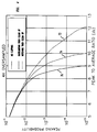
- FIG. 4 shows the results of simulations of different peak limiting scenarios comparing the peak to average power ratios (PAR) vs. peaking probability for a loaded single 1.25 MHz CDMA carrier, assuming a pilot with 40 other active walsh channels.
- the threshold was set at 8.5 dB above the average power, and the peaking probability is the probability that a peak will exceed the threshold. For example, a peaking probability of 10 -4 means that on average one in 10000 peaks will exceed the threshold.
- the plot 72 shows the PAR of the signal at about 11.3 dB measured at 10 -4 peaking probability.
- the plot 74 shows the PAR for the resulting signal in which peaks above the threshold are hardlimited to the threshold value then filtered.
- the resulting signal experiences about 1.2 dB of peak regrowth after filtering.
- hardlimiting was performed at 4X oversampling rate then filter with a cleanup filter.
- Plot 76 shows the results of the peak notching system which only exhibits about 0.3 dB of peak regrowth after the cleanup filtering at a peaking probability of 10 -4 .
- the performance degrades if the sampling rate is reduced to 2X. The reason is because the peaks are more likely to grow back in between the samples with the increased time span.
- the peak-notching algorithm has a peak regrowth of about 0.9 dB, approaching that of simple hardlimiting.
- adjustment or adjusting circuitry could directly adjust the peak sample on the signal path beyond the threshold to within the threshold or by a desired amount which is a function of the amount that the peak sample is reduced.
- the embodiment of the peak notching system has been described as being used to reduce the PAR of a CDMA 1.25 MHz carrier, but the peak notching system can be used to improve the PAR of other signals.
- the peak notching system has been described as producing a one sample adjustment, or notch, in the signal. A notch of multiple samples is possible which occurs when the adjusted or notched samples are adjusted to below adjacent samples.
- the peak notching system can be used with filters having different responses.
- the peak notching system can be used on digital or analog signals using digital and/or analog components.
- the peak notching system has been further described as using different configurations of particular components, but it should be understood that the peak notching system and portions thereof can be implemented in application specific integrated circuits, software-driven processing circuitry, firmware or other arrangements of discrete components as would be understood by one of ordinary skill in the art with the benefit of this disclosure. What has been described is merely illustrative of the application of the principles of the present invention. Those skilled in the art will readily recognize that these and various other modifications, arrangements and methods can be made to the present invention without strictly following the exemplary applications illustrated and described herein and without departing from the spirit and scope of the present invention.
Landscapes
- Physics & Mathematics (AREA)
- Nonlinear Science (AREA)
- Engineering & Computer Science (AREA)
- Power Engineering (AREA)
- Tone Control, Compression And Expansion, Limiting Amplitude (AREA)
- Dc Digital Transmission (AREA)
- Amplifiers (AREA)
- Control Of Amplification And Gain Control (AREA)
- Digital Transmission Methods That Use Modulated Carrier Waves (AREA)
- Analogue/Digital Conversion (AREA)
- Transmitters (AREA)
Abstract
Description
- This invention relates to communications systems, and more particularly to a system for reducing the peaks of a signal to be amplified.
- An ideal power amplifier amplifies an input signal of a given bandwidth with no waveshape alteration. The ideal power amplifier is therefore characterized as having a transfer function (input signal vs. output signal) which is linear with no transfer function discontinuities. In practice, a power amplifier, however, has a transfer function with nonlinear and "linear" regions. Whether the power amplifier is operating in a linear or nonlinear region depends on the amplitude of the input signal. For the power amplifier to achieve as near to linear operation as possible, the power amplifier is designed to operate within its linear region given the range of possible input signal amplitudes. If the input signal has an amplitude which causes the power amplifier to operate outside the linear region, the power amplifier introduces nonlinear components or distortion to the signal. When the input signal peak amplitude causes the amplifier to saturate (no appreciable increase in output amplitude with an increase in input amplitude) or to shut-off (no appreciable decrease in output amplitude with a decrease in input amplitude), the amplifier is being overdriven, and the output signal is clipped or distorted. Generally, an amplifier is characterized as having a clipping threshold, and input signals having amplitudes beyond the clipping threshold are clipped at the amplifier output. In addition to distorting the signal, the clipping or nonlinear distortion of the input signal causes power to be generated in adjacent channels or frequencies to corrupt or interfere with signals in the adjacent channels or frequencies, commonly referred to as spectral regrowth or adjacent channel power (ACP). The generation of adjacent channel power is of particular concern in wireless communications systems where signals being amplified are in adjacent channels or frequency bands.
- In communication systems where signals have a large range of amplitudes, components such as power amplifiers have to maintain linearity over a large dynamic range to avoid generating nonlinear distortion of the input signal and spectral adjacent channel power. For example in signals transmitted in the standard identified as EIA/TIA/IS-95 (Electronic Industries Association/Telecommunications Industry Association/Interim Standard 95) entitled "Mobile Station-Base Station Compatibility Standard for Dual-Mode Wideband Spread Spectrum Cellular System, March 1993 ("IS-95"), the peak to average power ratio (PAR) for a single loaded code division multiple access (CDMA) 1.25 MHz carrier is about 11.3 dB measured at 10-4 peaking probability (indicating a 1/10,000 chance that a peak exceeds a threshold value for example of 8.5 dB above the average power). As such, a high cost, low efficiency power amplifier is operated at an average power level far below its saturation point to avoid distorting the peaks and generating ACP. To reduce the cost and improve the efficiency of the power amplifier and other components, methods have been proposed for reducing the PAR of the signal without generating significant ACP or spectral regrowth which occurs when power from the signal appears at different frequency bands.
- A straight forward method for PAR reduction involves hardlimiting or hard clipping the signal peaks to a certain hardlimiting threshold to lower the PAR. A hard clipped signal, however, has abrupt edges and the short time duration of the clipped edges generates significant adjacent channel power and spectral regrowth in the frequency domain. A filter can be used to remove the ACP and the spectral regrowth. For a radio transmitter, the filter can be implemented at baseband or intermediate frequency (IF) where sharp filters are readily available either in digital or analog form. A digital implementation at baseband is favored because of its flexibility and low cost. It has been found, however, that after filtering the clipped signal, the signal peaks grow back. Accordingly, the peaks could be detected using the desired threshold, then the peaks above the detection threshold are hardlimited to a new limit lower than the detection threshold. When the peaks grow back alter the cleanup filtering, they would still be below the targeted value. For digital hardware implementation, this method is as easy to implement as the simple hardlimiting. However, the peaks that are slightly above the threshold only needs to be clipped lightly and their growth after cleanup filtering is also small. By clipping all these peaks to the new limit, the peaks that are slightly above the threshold can be over-clipped.
- U.S. Patent No. 5,287,387 discloses a window clipping method for reducing the peak to average power ratio of an input signal. In the window clipping process, an attenuating window is centered about a local maximum of a signal peak above a threshold, and the attenuating window is multiplied with the input signal to generate an attenuated signal. The attenuating window is comprised of multiple sample weights which are valued at less than one. The multiple weights of the attenuating window are multiplied with corresponding peak samples of the input signal to reduce the peak of the input signal to below a threshold. However, multiplying the signals in the time domain is equivalent to convolving the spectrum of the input signal with the window spectrum in the frequency domain, thereby altering the spectrum of the window clipped signal. Thus, the window clipping process fails to adequately address the problems of the hard clipping processes.
- The present invention reduces signal peaks by notching the peak of a signal above a threshold to produce a notched signal. The notched signal is then filtered to produce a resulting signal with a reduced peak amplitude. For example, in an implementation where the signal is represented by signal samples, the peak notching system first locates a peak sample that is beyond a threshold, such as a sample representing a positive peak sample of a peak above the threshold. Once a peak sample is located, the peak notching system adjusts the peak sample by an amount which is a function of the amount that the peak sample is beyond the threshold, effectively creating a notched signal with a one sample notch at the peak. The peak notching system filters the notched signal to fill in the notch to produce a signal with a reduced peak.
- Other aspects and advantages of the present invention may become apparent upon reading the following detailed description and upon reference to the drawings in which:
- FIGs. 1a-f show the operating of a hardlimiting process to reduce the PAR of an example waveform;
- FIGs. 2a-f show the operation of the peak notching system according to the principles of the present invention to reduce the peak of an example waveform;
- FIG. 3 shows a general block diagram of a peak notching system according to the principles of the present invention; and
- FIG. 4 shows a graphical representation of a comparison of different techniques for reducing the PAR of a signal.
-
- FIG. 1A shows an example baseband in-
phase waveform 2, such as a 1.25 MHz CDMA carrier, in the time domain with apeak 3 above athreshold 4, and FIG. 1B shows the corresponding spectral representation with theACP 5 being 45 dB below thesignal 2. FIG. 1C illustrates how the hard limiting procedure clips thesignal 2, and FIG. 1D shows the corresponding effect or increase in theACP 5 on the signal spectrum for a single carrier IS-95 system. However, after the clippedsignal 2 is filtered to reduce the ACP 5 as shown in FIG. 1F, thepeaks 7 grow back as shown in FIG. 1E. For example, if the limiting threshold is set at 8.5 dB above the average power, the resulting PAR is 9.5 dB after the filtering. In order to arrive at a PAR of 8.5 dB, the threshold has to be set to about 1.5 dB below the target, causing a large number of peaks that are below the targeted maximum to be clipped. - An illustrative embodiment of a peak notching system according to the principles of the present invention is described below which uses a simple and low-cost system to produce a signal with a reduced PAR while removing the adjacent channel power and spectral regrowth from the signal. FIG. 2A shows a
signal 10 to be amplified, and thesignal 10 is shown in the time domain with apeak 12 having an amplitude (for example voltage) above athreshold 14. FIG. 2B shows thesignal 10 in the frequency domain, such as a 1.25 MHz carrier which is 45 dB aboveadjacent channel power 16. Thesignal 10 is shown as an analog signal, but it should be understood that the peak notching system can sample thesignal 10 to obtain signal samples, shown as lines within the envelope of thesignal 10, which are used to represent thesignal 10. In this embodiment, the peak notching system locates apeak sample 18 representing the maximum of thepeak 12 above thethreshold 14. The peak notching system in this embodiment adjusts the amplitude (for example, the voltage) of thepeak sample 18 by an amount which is a function of the amount that the peak sample exceeds the threshold, effectively creating a notchedsignal 20 in the time domain with a one-sample notch 22 at the top of the peak 12 as shown in FIG. 2C. In the frequency domain shown in FIG. 2D, theadjacent channel power 16 increases due to the notching of thesignal 10 to produce the notchedsignal 20. The notching of thesignal 10 reduces the in-band power or energy of the signal and increases the out-of-band power or energy. To reduce the adjacent channel power and bring the reducedpeak sample 18 to thethreshold 14, the notchedsignal 20 is filtered to fill in the notch and produce asignal 24 shown with a reduced PAR as shown in FIG. 2E and with reduced adjacent channel power as shown in FIG. 2F. The filter reduces the power or energy outside the band and passes or retains the in-band power or energy. As such, by filtering the notched signal, the out-of band power produced by the notching is removed, and the resulting signal has an amplitude adjusted by an amount depending on the amount that the original peak sample is beyond the threshold. - As mentioned above, the amount by which the peak sample is adjusted is a function of the amount that the peak sample exceeds the threshold. Depending on the embodiment, the amount that the peak sample is reduced can be determined as a function of the amount that the peak sample exceeds the threshold and a scaling factor. In this embodiment, the scaling factor is dependent on the oversampling ratio. The sampling rate is the rate at which the signal is sampled. If a waveform is sampled at twice the highest frequency sine wave component, then the original signal can be reconstructed from the sample points. As such, the minimum sampling rate would be 2 times the frequency of the signal. The oversampling ratio can be determined by the sampling rate + minimum sampling rate required to reconstruct the signal or 2. In this embodiment, a sampling rate of 8 times the frequency of the signal is performed which provides an oversampling ratio of 4. For an oversampling ratio of 4, the scaling factor is approximately 4. If a greater oversampling ratio is used, the scaling factor would increase, and if the oversampling ratio decreases, the scaling factor decreases. In this embodiment, with an oversampling ratio of 4, an adjustment value equal to about 4 X the amount that the peak sample is above the threshold is subtracted from the peak sample to produce a notched signal. If the peak sample has a negative polarity, the adjustment value is added to the peak sample. Other embodiments are possible using different scaling factors to determine the adjustment value or using an adjustment value determined in a different manner to reduce the peak sample in different ways.
- FIG. 3 shows an embodiment of a
peak notching system 30 for notching positive peaks of a signal on asignal path 34. In this embodiment, thepeak notching system 30 locates a peak sample (such as a positive or negative peak sample) in the digital domain using a peaksample location circuitry 36. In this embodiment, the peaksample location circuitry 36 includes afirst delay 38 and asecond delay 40 on thesignal path 34. To locate a peak sample, the sample at the output of thefirst delay 38 or the potential peak sample is compared with the preceding sample at the output of thesecond delay 40 and with the following sample at the input of thedelay 38. In this embodiment, asummer 42 subtracts the following sample at the input to thedelay 38 from the sample at the output of thedelay 38. If the result is negative, then the following sample is greater than the sample at the output of thedelay 38. If the result is positive, then the following sample is less than the sample at the output of thedelay 38. Asummer 44 subtracts the sample at the output of thedelay 38 from the preceding sample at the output of thedelay 40. If the result is negative, the sample at the output of thedelay 38 is greater than the sample at the output of thedelay 40. If the result is positive, the sample at the output of thedelay 38 is less than the sample at the output of thedelay 40. - A peak sample is located by comparing the sample at the output of the
delay 38 with the preceding and following samples. If the following sample at the input to thedelay 38 is less than the potential peak sample at the output of thedelay 38 and the potential peak sample is greater than the preceding sample at the output of thedelay 40, the potential peak sample is a positive peak sample. If the following sample at the input to thedelay 38 is greater than the potential peak sample and the potential peak sample is less than the preceding sample at the output of thedelay 40, the potential peak sample is a negative peak sample. The sign bits resulting from the operations of thesummers gate 48. - In this embodiment, the
peak notching system 30 includesthreshold detection circuitry 49 to detect whether the potential peak sample is above a threshold, indicating a positive peak. In limiting negative peaks, similar circuitry (not shown) for detecting whether a sample is below a negative threshold would be used along with additional circuitry to adjust a negative peak sample below the negative threshold to be above the threshold as would be understood by one of skill in the art with the benefit of this disclosure. In this embodiment, the output of thedelay 38 is compared to athreshold 50. For example, the sample at the output of thedelay 38 can be subtracted from thethreshold 50 by an adder 52. If the threshold value is greater than the sample value at the output of thedelay 38, the sample value is not located above the threshold, and the resulting sign bit is a logic "0" which is provided to the ANDgate 48. If the threshold value is less than the sample at the output of thedelay 38, the potential peak sample is located above the threshold, and the summer 52 produces a negative value. The negative sign bit which is a logic "1" is provided to the ANDgate 48. - In this embodiment, if either the adder 52 produces a "0" (indicating a sample below the threshold) or the XOR gate 46 produces a logic "0" (sample at output of the
delay 38 not a peak sample), the ANDgate 48 produces a zero (indicating not a positive peak sample). As such, switching or adjustingcircuitry 56 provides the sample at the output of thedelay 38 as an output without the sample being altered or replaced. In this embodiment, the output from the ANDgate 48 controls amultiplexer 57. If the AND gate produces a "0," themultiplexer 57 provides the sample at the output of thedelay 38 as an output to themultiplier 57 without the sample being altered or replaced by the shown circuitry of thesystem 30. The sample at the output of thedelay 38 is produced after passing through thedelay 40. Adelay 58 delays the control signal from the ANDgate 48 by an amount corresponding to thedelay 40, so the sample at the output of thedelay 38 is received by themultiplexer 57 at the time the signal from the ANDgate 48 is received by themultiplexer 57. As such, themultiplexer 57 produces the appropriate sample value at the appropriate time. - If the sample at the output of the
delay 38 is a positive peak sample, thepeak notching system 30 notches the peak by adjusting the positive peak sample by an adjustment value. In this embodiment, if the output of the XOR gate 46 is a one (indicating a peak sample) and the sign bit from the output of the summer 52 is a one (indicating a sample above the threshold), the sample at the output of thedelay 38 is a positive peak sample. As such, the switching or adjustingcircuitry 56 provides an adjusted sample instead of the positive peak sample. In this embodiment, if the ANDgate 48 produces a "1," themultiplexer 57 switches in an adjusted or reduced positive peak sample from adjustment or adjustedsample circuitry 60. Theadjustment circuitry 60 receives the sample at the output of thedelay 38. In this embodiment, the adder 52 receives the sample and provides the difference between the sample value and the threshold to amultiplier 62. Themultiplier 62 calculates an adjustment value, for example 4 times the difference between the sample and the threshold. The sample is also provided to anadder 64 which subtracts the adjustment value from the sample to produce a reduced sample. If the sample is a positive peak sample, the reduced sample from theadjustment circuitry 60 is produced to replace the positive peak sample at the output of thedelay 38 after passing through adelay 66. Thedelay 66 delays the reduced sample by an amount corresponding to thedelay 40 and thedelay 58. As such, the reduced sample is received by themultiplexer 57 at the same time as the corresponding control signal from the ANDgate 48 and the corresponding positive peak sample from the output of thedelay 38. - By switching in the reduced sample to the signal path, a notched signal is produced. The notching of the signal increases the adjacent channel power, but a
downstream filter 70 can reduce the adjacent channel power while passing the in-band power. As such, the notch is filled in to produce a signal with reduced adjacent channel power and a reduced peak to average power ratio because the peak of the resulting signal has an amplitude reduced by an amount which is a function of the amount that the peak sample is reduced. The filter can be a finite impulse response filter (FIR) filter operated in the digital domain or in the analog domain after the signal has been digital-to-analog converted. Thepeak notching system 30 is simple and cost effective, for example requiring a very small amount of space on a field programmable gate array (FPGA). - FIG. 4 shows the results of simulations of different peak limiting scenarios comparing the peak to average power ratios (PAR) vs. peaking probability for a loaded single 1.25 MHz CDMA carrier, assuming a pilot with 40 other active walsh channels. The threshold was set at 8.5 dB above the average power, and the peaking probability is the probability that a peak will exceed the threshold. For example, a peaking probability of 10-4 means that on average one in 10000 peaks will exceed the threshold. The
plot 72 shows the PAR of the signal at about 11.3 dB measured at 10-4 peaking probability. Theplot 74 shows the PAR for the resulting signal in which peaks above the threshold are hardlimited to the threshold value then filtered. At 10-4 peaking probability, the resulting signal experiences about 1.2 dB of peak regrowth after filtering. In this embodiment, hardlimiting was performed at 4X oversampling rate then filter with a cleanup filter.Plot 76 shows the results of the peak notching system which only exhibits about 0.3 dB of peak regrowth after the cleanup filtering at a peaking probability of 10-4. The performance degrades if the sampling rate is reduced to 2X. The reason is because the peaks are more likely to grow back in between the samples with the increased time span. At 2X sampling rate, the peak-notching algorithm has a peak regrowth of about 0.9 dB, approaching that of simple hardlimiting. - In addition to the embodiment described above, alternative configurations of the peak notching system according to the principles of the present invention are possible which omit and/or add components and/or use variations or portions of the described system. For example, for notching signals of positive and negative peaks, an embodiment could use two (2)
such systems 30 or at least 2 sets, variations or portions of the describedsystem 30 as would be understood by one skilled in the art to adjust positive or negative peaks beyond a threshold. The signal on thesignal path 34 can be a stream of so-called in-phase (I) or quadrature (Q) digital signal samples. To adjust positive and negative peaks of both I and Q signals, an embodiment could use four (4)such systems 30 or at least 4 sets, variations or portions of the describedsystem 30 as would be understood by one skilled in the art. Furthermore, instead of using switchingcircuitry 56 to replace the peak sample with an adjusted sample, adjustment or adjusting circuitry could directly adjust the peak sample on the signal path beyond the threshold to within the threshold or by a desired amount which is a function of the amount that the peak sample is reduced. Additionally, the embodiment of the peak notching system has been described as being used to reduce the PAR of a CDMA 1.25 MHz carrier, but the peak notching system can be used to improve the PAR of other signals. The peak notching system has been described as producing a one sample adjustment, or notch, in the signal. A notch of multiple samples is possible which occurs when the adjusted or notched samples are adjusted to below adjacent samples. Depending on the embodiment, the peak notching system can be used with filters having different responses. - The system has been described as using a particular configuration of components, but other devices or arrangements can be used as well which perform the same functions. For example, the peak notching system can be used on digital or analog signals using digital and/or analog components. The peak notching system has been further described as using different configurations of particular components, but it should be understood that the peak notching system and portions thereof can be implemented in application specific integrated circuits, software-driven processing circuitry, firmware or other arrangements of discrete components as would be understood by one of ordinary skill in the art with the benefit of this disclosure. What has been described is merely illustrative of the application of the principles of the present invention. Those skilled in the art will readily recognize that these and various other modifications, arrangements and methods can be made to the present invention without strictly following the exemplary applications illustrated and described herein and without departing from the spirit and scope of the present invention.
Claims (16)
- A method for use in a communications system including a signal to be amplified, said method comprising:notching a peak of said signal beyond a threshold to produce a notched signal; andfiltering said notched signal to produce a resulting signal having a reduced peak amplitude compared to said signal.
- The method of claim 1 wherein said notching includes:locating a peak sample; andadjusting said peak sample to within said threshold.
- The method of claim 2 wherein said adjusting includes:adjusting said peak sample by an amount which is a function of the amount that said peak sample is beyond said threshold.
- The method of claim 2 wherein said locating includes:determining whether a sample of said signal is a positive peak sample or a negative peak sample; andcomparing said sample with said threshold.
- The method of claim 4 wherein said determining includes:comparing said sample with a preceding sample and a following sample of said signal.
- The method of claim 3 wherein said adjusting includes:determining said amount as a function of the difference between said threshold and said peak sample and an oversampling factor;adjusting said peak sample by said amount to produce an adjusted sample; andreplacing said peak sample with said adjusted sample.
- A system for limiting the peak of a signal to be amplified, said system comprises:notching circuitry configured to notch a peak of said signal above a threshold to produce a notched signal; anda filter filters said notched signal to produce a signal within said threshold.
- The system of claim 7 wherein said notching circuitry includes:peak sample locating circuitry configured to locate a peak sample.
- The system of claim 7 wherein said notching circuitry including:a first delay coupled to a second delay, said first delay receives a preceding sample while producing a sample, said second delay receives said sample while producing a following sample;a peak sample locating circuitry configured to determine whether said sample is a peak sample by comparing said sample with said preceding sample and said following sample;threshold detection circuitry determines if said sample is above said threshold; andadjustment circuitry responsive to said sample to determine an adjustment value, said sample being reduced by an adjustment value to produce an adjusted sample.
- The system of claim 9 including:switching circuitry responsive to whether said sample is a peak sample and beyond a threshold to replace said sample with said adjusted sample.
- A method for processing a signal to be amplified having at least one peak beyond a threshold and a frequency band, said method comprising:notching a peak of said signal beyond a threshold by an adjustment amount which is a function of the amount said peak is beyond said threshold; andfiltering said notched signal to remove energy outside said frequency band while passing energy within said frequency band.
- The method of claim 11 wherein said notching includes:locating a peak sample; andadjusting said peak sample to within said threshold.
- The method of claim 12 wherein said locating includes:determining whether a sample of said signal is a positive peak sample or a negative peak sample; andcomparing said sample with said threshold.
- The method of claim 12 wherein said locating includes:determining whether a sample of said signal is a positive peak sample or a negative peak sample; andcomparing said sample with said threshold.
- A method for processing a signal to be amplified, said method comprising:notching a peak of said signal beyond a threshold; andfiltering said notched signal to produce a resulting signal within said threshold.
- The method of claim 12 wherein said notching includes:determining whether a sample is a peak sample;comparing said sample with said threshold; andadjusting said peak sample above said threshold by an amount which is a function of the amount said peak sample exceeds said threshold.
Applications Claiming Priority (2)
| Application Number | Priority Date | Filing Date | Title |
|---|---|---|---|
| US09/363,329 US6654427B1 (en) | 1999-07-28 | 1999-07-28 | Signal notching system for limiting signal peaks |
| US363329 | 1999-07-28 |
Publications (3)
| Publication Number | Publication Date |
|---|---|
| EP1073196A2 true EP1073196A2 (en) | 2001-01-31 |
| EP1073196A3 EP1073196A3 (en) | 2006-07-19 |
| EP1073196B1 EP1073196B1 (en) | 2013-05-22 |
Family
ID=23429777
Family Applications (1)
| Application Number | Title | Priority Date | Filing Date |
|---|---|---|---|
| EP00306070.4A Expired - Lifetime EP1073196B1 (en) | 1999-07-28 | 2000-07-17 | Signal notching system for limiting signal peaks |
Country Status (6)
| Country | Link |
|---|---|
| US (1) | US6654427B1 (en) |
| EP (1) | EP1073196B1 (en) |
| JP (1) | JP4436545B2 (en) |
| KR (1) | KR100685567B1 (en) |
| AU (1) | AU4878700A (en) |
| CA (1) | CA2314555C (en) |
Cited By (1)
| Publication number | Priority date | Publication date | Assignee | Title |
|---|---|---|---|---|
| WO2002089315A3 (en) * | 2001-04-25 | 2003-11-06 | Filtronic Plc | Electrical signal pre-conditioning |
Families Citing this family (9)
| Publication number | Priority date | Publication date | Assignee | Title |
|---|---|---|---|---|
| US6931053B2 (en) * | 1998-11-27 | 2005-08-16 | Nortel Networks Limited | Peak power and envelope magnitude regulators and CDMA transmitters featuring such regulators |
| DE60108423T2 (en) * | 2000-08-01 | 2005-12-22 | Telefonaktiebolaget Lm Ericsson (Publ) | AMPLITUDE LIMIT |
| JP3796204B2 (en) * | 2002-07-31 | 2006-07-12 | 松下電器産業株式会社 | Multi-carrier transmission signal peak suppression method and multi-carrier transmission signal generation circuit having peak suppression function |
| US7356186B2 (en) * | 2002-08-23 | 2008-04-08 | Kulas Charles J | Digital representation of audio waveforms using peak shifting to provide increased dynamic range |
| DE60200378T2 (en) * | 2002-08-30 | 2004-09-16 | Alcatel | Signal peak scaling method and corresponding transmitter |
| US7362819B2 (en) * | 2004-06-16 | 2008-04-22 | Lucent Technologies Inc. | Device and method for reducing peaks of a composite signal |
| FI20055012A0 (en) * | 2005-01-07 | 2005-01-07 | Nokia Corp | Trimming a broadcast signal |
| EP2043316A1 (en) * | 2007-09-28 | 2009-04-01 | Lucent Technologies Inc. | A method for peak limiting of transmit power for radio transmission, a transmitter, a base station, a mobile station and a communication network therefor |
| US20250233785A1 (en) * | 2024-01-17 | 2025-07-17 | Nokia Solutions And Networks Oy | Peak to average power ratio reduction |
Citations (1)
| Publication number | Priority date | Publication date | Assignee | Title |
|---|---|---|---|---|
| US5727026A (en) | 1995-11-15 | 1998-03-10 | Motorola, Inc. | Method and apparatus for peak suppression using complex scaling values |
Family Cites Families (4)
| Publication number | Priority date | Publication date | Assignee | Title |
|---|---|---|---|---|
| US5287387A (en) | 1992-03-06 | 1994-02-15 | Motorola, Inc. | Low splatter peak-to-average signal reduction |
| CA2125468C (en) * | 1993-06-28 | 1998-04-21 | Danny Thomas Pinckley | Method of selectively reducing spectral components in a wideband radio frequency signal |
| JP2718398B2 (en) * | 1995-06-30 | 1998-02-25 | 日本電気株式会社 | CDMA base station transmitter |
| US6166598A (en) * | 1999-07-22 | 2000-12-26 | Motorola, Inc. | Power amplifying circuit with supply adjust to control adjacent and alternate channel power |
-
1999
- 1999-07-28 US US09/363,329 patent/US6654427B1/en not_active Expired - Lifetime
-
2000
- 2000-07-17 EP EP00306070.4A patent/EP1073196B1/en not_active Expired - Lifetime
- 2000-07-20 CA CA002314555A patent/CA2314555C/en not_active Expired - Fee Related
- 2000-07-24 AU AU48787/00A patent/AU4878700A/en not_active Abandoned
- 2000-07-26 JP JP2000224838A patent/JP4436545B2/en not_active Expired - Fee Related
- 2000-07-27 KR KR1020000043392A patent/KR100685567B1/en not_active Expired - Fee Related
Patent Citations (1)
| Publication number | Priority date | Publication date | Assignee | Title |
|---|---|---|---|---|
| US5727026A (en) | 1995-11-15 | 1998-03-10 | Motorola, Inc. | Method and apparatus for peak suppression using complex scaling values |
Cited By (2)
| Publication number | Priority date | Publication date | Assignee | Title |
|---|---|---|---|---|
| WO2002089315A3 (en) * | 2001-04-25 | 2003-11-06 | Filtronic Plc | Electrical signal pre-conditioning |
| US7330704B2 (en) | 2001-04-25 | 2008-02-12 | Filtronic Plc | Electrical signal pre-conditioning |
Also Published As
| Publication number | Publication date |
|---|---|
| JP2001094371A (en) | 2001-04-06 |
| EP1073196B1 (en) | 2013-05-22 |
| CA2314555C (en) | 2003-12-02 |
| US6654427B1 (en) | 2003-11-25 |
| KR100685567B1 (en) | 2007-02-22 |
| KR20010021140A (en) | 2001-03-15 |
| EP1073196A3 (en) | 2006-07-19 |
| CA2314555A1 (en) | 2001-01-28 |
| AU4878700A (en) | 2001-02-01 |
| JP4436545B2 (en) | 2010-03-24 |
Similar Documents
| Publication | Publication Date | Title |
|---|---|---|
| Armstrong | New OFDM peak-to-average power reduction scheme | |
| US20200021319A1 (en) | System and method for increasing bandwidth for digital predistortion in multi-channel wideband communication systems | |
| CA2262361C (en) | Method and apparatus for tailored distortion of a signal prior to amplification | |
| US5696794A (en) | Method and apparatus for conditioning digitally modulated signals using channel symbol adjustment | |
| US20090285194A1 (en) | Efficient Peak Cancellation Method for Reducing the Peak-To-Average Power Ratio in Wideband Communication Systems | |
| US20040076247A1 (en) | Peak-to-average power ratio modifier | |
| EP1195892A1 (en) | Method and corresponding transmitter for predistorting a wideband radio signal to avoid clipping | |
| EP1471659B1 (en) | Code division multiple access base station transmitter | |
| US20110059710A1 (en) | Dynamic crest factor reduction system | |
| KR100605440B1 (en) | Amplitude Limitation in Code Division Multiple Access Systems | |
| EP1396970B1 (en) | Method for scaling signal peaks and corresponding transmitter | |
| WO2003075457A2 (en) | Apparatus and method for reducing peak-to-average signal power ratio | |
| US6654427B1 (en) | Signal notching system for limiting signal peaks | |
| EP1360760B1 (en) | Amplitude limitation | |
| EP0888675A1 (en) | Method and apparatus for conditioning modulated signals using window expansion | |
| Väänänen et al. | Simple algorithm for peak windowing and its application in GSM, EDGE and WCDMA systems | |
| US10778153B2 (en) | Crest factor reduction in power amplifier circuits | |
| KR20020009571A (en) | Decresting peaks in a cdma signal | |
| JP3702829B2 (en) | Peak factor reduction device | |
| CN1716933B (en) | A Method for Realizing CDMA Signal Clipping | |
| JP4288458B2 (en) | Amplitude limiting circuit and CDMA communication apparatus | |
| EP1402633B1 (en) | Data transmission method and arrangement | |
| da Silva et al. | A Novel Limiter with Application in Crest Factor Reduction Techniques for Wireless Communications |
Legal Events
| Date | Code | Title | Description |
|---|---|---|---|
| PUAI | Public reference made under article 153(3) epc to a published international application that has entered the european phase |
Free format text: ORIGINAL CODE: 0009012 |
|
| AK | Designated contracting states |
Kind code of ref document: A2 Designated state(s): AT BE CH CY DE DK ES FI FR GB GR IE IT LI LU MC NL PT SE |
|
| AX | Request for extension of the european patent |
Free format text: AL;LT;LV;MK;RO;SI |
|
| PUAL | Search report despatched |
Free format text: ORIGINAL CODE: 0009013 |
|
| AK | Designated contracting states |
Kind code of ref document: A3 Designated state(s): AT BE CH CY DE DK ES FI FR GB GR IE IT LI LU MC NL PT SE |
|
| AX | Request for extension of the european patent |
Extension state: AL LT LV MK RO SI |
|
| 17P | Request for examination filed |
Effective date: 20070105 |
|
| AKX | Designation fees paid |
Designated state(s): DE FI FR GB SE |
|
| 17Q | First examination report despatched |
Effective date: 20071102 |
|
| RAP3 | Party data changed (applicant data changed or rights of an application transferred) |
Owner name: LUCENT TECHNOLOGIES INC. |
|
| RAP1 | Party data changed (applicant data changed or rights of an application transferred) |
Owner name: ALCATEL LUCENT |
|
| GRAP | Despatch of communication of intention to grant a patent |
Free format text: ORIGINAL CODE: EPIDOSNIGR1 |
|
| GRAS | Grant fee paid |
Free format text: ORIGINAL CODE: EPIDOSNIGR3 |
|
| GRAA | (expected) grant |
Free format text: ORIGINAL CODE: 0009210 |
|
| AK | Designated contracting states |
Kind code of ref document: B1 Designated state(s): DE FI FR GB SE |
|
| REG | Reference to a national code |
Ref country code: GB Ref legal event code: FG4D |
|
| REG | Reference to a national code |
Ref country code: DE Ref legal event code: R096 Ref document number: 60048024 Country of ref document: DE Effective date: 20130718 |
|
| REG | Reference to a national code |
Ref country code: FR Ref legal event code: GC Effective date: 20130802 |
|
| 111Z | Information provided on other rights and legal means of execution |
Free format text: DE FI FR GB SE Effective date: 20130410 |
|
| REG | Reference to a national code |
Ref country code: GB Ref legal event code: 732E Free format text: REGISTERED BETWEEN 20130919 AND 20130925 |
|
| PG25 | Lapsed in a contracting state [announced via postgrant information from national office to epo] |
Ref country code: FI Free format text: LAPSE BECAUSE OF FAILURE TO SUBMIT A TRANSLATION OF THE DESCRIPTION OR TO PAY THE FEE WITHIN THE PRESCRIBED TIME-LIMIT Effective date: 20130522 Ref country code: SE Free format text: LAPSE BECAUSE OF FAILURE TO SUBMIT A TRANSLATION OF THE DESCRIPTION OR TO PAY THE FEE WITHIN THE PRESCRIBED TIME-LIMIT Effective date: 20130522 |
|
| PLBE | No opposition filed within time limit |
Free format text: ORIGINAL CODE: 0009261 |
|
| STAA | Information on the status of an ep patent application or granted ep patent |
Free format text: STATUS: NO OPPOSITION FILED WITHIN TIME LIMIT |
|
| 26N | No opposition filed |
Effective date: 20140225 |
|
| REG | Reference to a national code |
Ref country code: DE Ref legal event code: R097 Ref document number: 60048024 Country of ref document: DE Effective date: 20140225 |
|
| REG | Reference to a national code |
Ref country code: FR Ref legal event code: PLFP Year of fee payment: 16 |
|
| REG | Reference to a national code |
Ref country code: FR Ref legal event code: PLFP Year of fee payment: 17 |
|
| REG | Reference to a national code |
Ref country code: FR Ref legal event code: PLFP Year of fee payment: 18 |
|
| PGFP | Annual fee paid to national office [announced via postgrant information from national office to epo] |
Ref country code: GB Payment date: 20170719 Year of fee payment: 18 Ref country code: DE Payment date: 20170724 Year of fee payment: 18 Ref country code: FR Payment date: 20170724 Year of fee payment: 18 |
|
| REG | Reference to a national code |
Ref country code: DE Ref legal event code: R119 Ref document number: 60048024 Country of ref document: DE |
|
| GBPC | Gb: european patent ceased through non-payment of renewal fee |
Effective date: 20180717 |
|
| PG25 | Lapsed in a contracting state [announced via postgrant information from national office to epo] |
Ref country code: DE Free format text: LAPSE BECAUSE OF NON-PAYMENT OF DUE FEES Effective date: 20190201 Ref country code: FR Free format text: LAPSE BECAUSE OF NON-PAYMENT OF DUE FEES Effective date: 20180731 Ref country code: GB Free format text: LAPSE BECAUSE OF NON-PAYMENT OF DUE FEES Effective date: 20180717 |