BACKGROUND OF THE INVENTION
-
This invention relates to an organic
electroluminescent device (organic EL device) wherein an
organic layer having a luminescent or light-emitting
region is provided between an anode and a cathode.
-
Lightweight, highly efficient flat panel displays
have been extensively studied and developed, for example,
for picture display of computers and television sets.
-
Since cathode-ray tubes (CRT) are high in luminance
and exhibit good color reproducibility, they are most
widely employed for display at present. Nevertheless, the
problems are involved in that the tubes are bulky, heavy
and high in power consumption.
-
For lightweight, highly efficient flat panel
displays, there have now been put on the market liquid
crystal displays of the active matrix drive type. However,
liquid crystal displays have the problems that their
angle of field is narrow, they do not rely on spontaneous
light and thus, need great power consumption for back
light when placed in a dark environment, and they do not
have a satisfactory response to high-speed video signals
of high fineness which have been expected as being in
practical use in future. Especially, a difficulty is
involved in making a liquid crystal display with a large
picture plane size, along with a problem on its high
production costs.
-
As a substitute therefor, a display of the type
using a light-emitting diode may be possible, but such a
display is also high in production costs, coupled with
another problem that it is difficult to form a matrix
structure of light-emitting diodes on one substrate. Thus,
when considered as a candidate for a low-cost display
used in place of CRTs, this type of display has a great
problem to solve before putting to practical use.
-
As a flat panel display which has the possibility
of solving these problems, attention has been recently
paid to organic electroluminescent devices (organic EL
devices) using organic luminescent materials. More
particularly, when using organic compounds as a
luminescent material, it has been expected to realize a
flat panel display, which makes use of spontaneous light,
has a high response speed and has no dependence on an
angle of field.
-
The organic electroluminescent device is so
arranged that an organic thin film, which contains a
luminescent material capable of emitting light through
charge of an electric current, is formed between an
optically transparent anode and a metallic cathode. In
the research report published in Applied Physics Letters,
Vol. 51, No. 12, pp. 913 - 915 (1987), C. W. Tang and S.
A. VanSlyke set forth a device structure (an organic EL
device having a single hetero structure), which has a
double-layered structure including, as organic thin films,
a thin film composed of a hole transport material and a
thin film composed of an electron transport material. In
the device, luminescence occurs by re-combination of
holes and electrons injected from the respective
electrodes into the organic films.
-
In this device structure, either of the hole
transport material or the electron transport material
serves also as a luminescent material. Luminescence takes
place in a wavelength band corresponding to the energy
gap between the ground state and the energized state of
the luminescent material. When using such a double-layered
structure, a drive voltage can be remarkably
reduced, along with an improved luminescent efficiency.
-
Since then, there has been developed a three-layered
structure (organic EL device having a double
hetero structure) of a hole transport material, a
luminescent material and an electron transport material
as set out in the research report of C. Adachi, S. Tokita,
T. Tsutsui and S. Saito, published in Japanese Journal of
Applied Physics, Vol. 27, No. 2, pp. L269 - L271 (1988).
Moreover, a device structure comprising a luminescent
material present in an electron transport material has
been developed as set out in the research report of C. W.
Tang, S. A. VanSlyke and C. H. Chen published in Journal
of Applied Physics, Vol. 65, No. 9, pp. 3610 - 3616
(1989). Through these researches, evidence has been given
to the possibility of luminescence of high luminance at
low voltage, thus leading to recent, very extensive
studies and developments.
-
Organic compounds used as a luminescent material
are considered to be advantageous in that because of
their diversity in kind, a luminescent color can be
arbitrarily changed theoretically by changing their
molecular structure. Accordingly, it may be easier in
comparison with thin film EL devices using inorganic
materials to provide, via proper molecular design, three
colors of R (red), G (green) and B (blue) having good
color purities necessary for full color displays.
-
However, organic electroluminescent devices still
have problems to solve. More particularly, a difficult is
involved in the development of a stable red luminescent
device with high luminance. In an instance of red
luminescence attained by doping DCM [4-dicyanomethylene-6-(p-dimethylaminostyryl)-2-methyl-4H-pyran]
in tris(8-quinolinol)aluminium
(hereinafter abbreviated as Alq3) for
use as a currently reported electron transport material,
this is not satisfactory as a display material with
respect to both maximum luminance and reliability.
-
BSB-BCN, which was reported by T. Tsutsui and D. U.
Kim in the meeting of Inorganic and Organic
Electroluminescence (at Berlin, 1996), is able to realize
a luminance as high as 1000 cd/m2 or over, but is not
always perfect with respect to the chromaticity for use
as a red color for full color display.
-
It is now demanded how to realize a red luminescent
device which is high in luminance, stable and high in
color purity.
-
In Japanese Patent Laid-open No. Hei 7-188649
(Japanese Patent Application No. Hei 6-148798), it has
been proposed to use a specific type of distyryl compound
as an organic electroluminescent material. However, the
intended luminescent color is blue, not red.
SUMAMRY OF THE INVENTION
-
An object of the invention is to provide an organic
electroluminescent device, which ensures a high luminance
and stable red luminescence.
-
Intensive studies have been made in order to solve
the above-stated problems of the prior art, and as a
result, it has been found that when using a specific type
of styryl compound as a luminescent material, there can
be provided a highly reliable red luminescent device,
which is very useful for realizing a stable full color
display of high luminance.
-
More particularly, there is provided, according to
the invention, an organic electroluminescent device of
the type which comprises an organic layer which has a
luminescent region and is provided between an anode and a
cathode and which contains, as an essential component, an
organic material capable of generating luminescence by
application of an electric current, wherein the organic
layer contains, as an organic luminescent material, at
least one julolidyl-substituted styryl compound
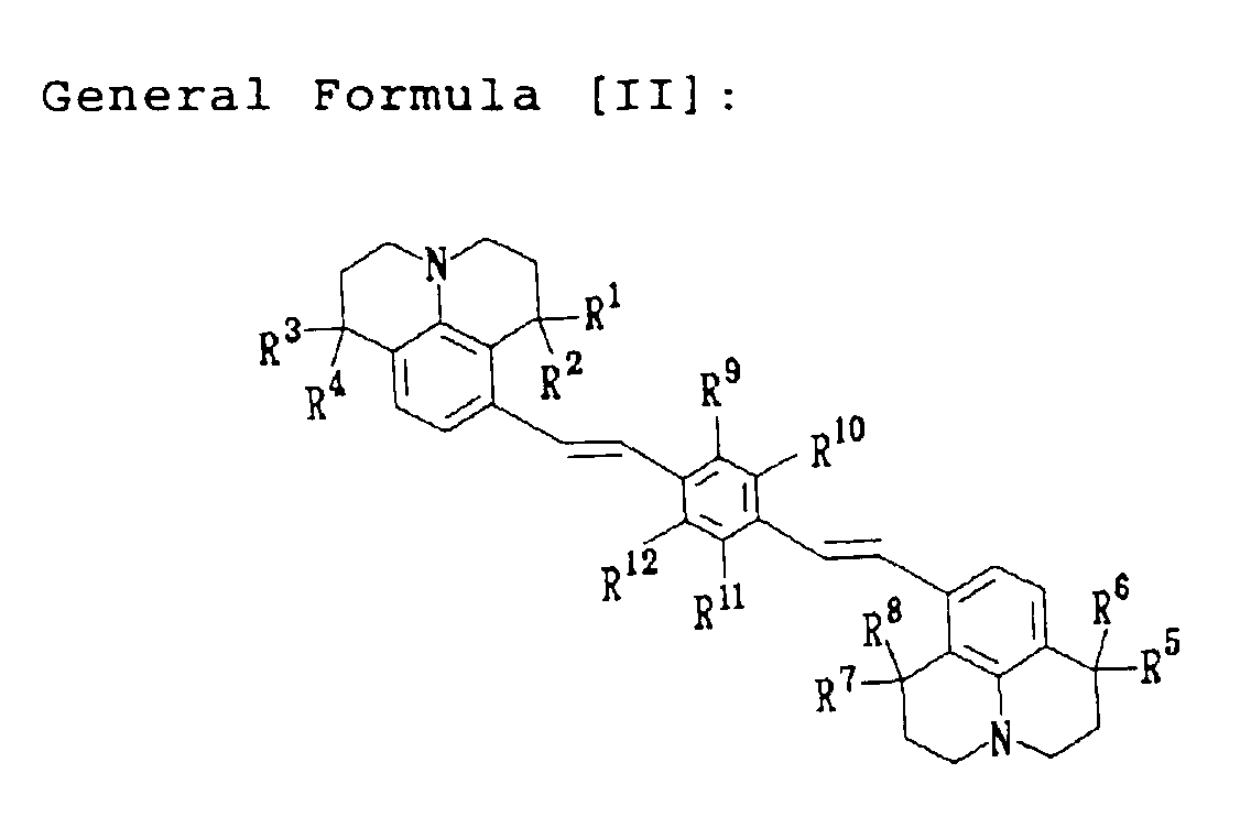
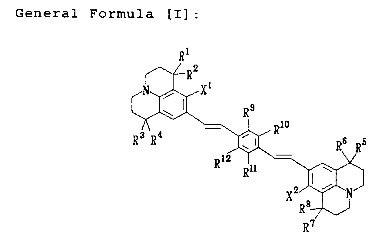
represented by the following general formula [I] or [II]:
wherein X
1 and X
2 may be the same or different and,
respectively, represent a hydrogen atom, a hydroxyl group
or a saturated or unsaturated, unsubstituted or
substituted alkoxyl group, which preferably has 1 to 6
carbon atoms, e.g., a methoxy group, an ethoxy group, a
methoxymethoxy group or the like, an alkyl group, which
preferably has 1 to 6 carbon atoms, e.g., a methyl group,
an ethyl group or the like, an amino group, an alkylamino
group, which preferably has 1 to 6 carbon atoms, e.g., a
methylamino group, an ethyl amino group or the like, or a
substituted or unsubstituted aryl group such as a phenyl
group, a naphthyl group or the like, and R
1, R
2, R
3, R
4, R
5,
R
6, R
7 and R
8 may be the same or different and
independently represent a lower alkyl group, which
preferably has 1 to 6 carbon atoms, e.g., a methyl group,
an ethyl group or the like, R
9, R
10, R
11 and R
12 may be the
same or different and at least one of them represents an
electron attracting group, i.e., at least one of them
represents a cyano group, a nitro group or a halogen atom
such as a chlorine atom, a fluorine atom or the like.
-
The use, as a luminescent material, of the
julolidyl-substituted styryl compound of the above
general formula [I] or [II] enables one not only to
obtain stable red luminescence of high luminance, but
also to provide a device which has electrically,
thermally or chemically excellent stability. The styryl
compounds of the general formula [I] and [II] may be used
singly or in combination.
BRIEF DESCRIPTION OF THE DRAWINGS
-
- Fig. 1 is a schematic sectional view showing an
essential part of an organic electroluminescent device
according to one embodiment of the invention;
- Fig. 2 is a schematic sectional view showing an
essential part of an organic electroluminescent device
according to another embodiment of the invention;
- Fig. 3 is schematic sectional view showing an
essential part of an organic electroluminescent device
according to a further embodiment of the invention;
- Fig. 4 is a schematic sectional view showing an
essential part of an organic electroluminescent device
according to a still further embodiment of the invention;
- Fig. 5 is a view showing an arrangement of a full
color flat display using an organic electroluminescent
device of the invention;
- Fig. 6 is a 1H NMR spectrogram of a julolidyl-substituted
styryl compound (9a) (or structural formula
((1)-1) usable in the invention;
- Fig. 7 is a 1H NMR spectrogram of a julolidyl-substituted
styryl compound (9b) (or structural formula
((1)-8) usable in the invention;
- Fig. 8 is a 1H NMR spectrogram of a julolidyl-substituted
styryl compound (8) (or structural formula
((1)-6) usable in the invention;
- Fig. 9 is an emission spectrogram of an organic
electroluminescent device of Example 1 of the invention;
- Fig. 10 is a graph showing a voltage-luminance
characteristic of the organic electroluminescent device
of Example 1 of the invention;
- Fig. 11 is an emission spectrogram of an organic
electroluminescent device of Example 2 of the invention;
- Fig. 12 is a graph showing a voltage-luminance
characteristic of an organic electroluminescent device of
Example 2 of the invention;
- Fig. 13 is an emission spectrogram of an organic
electroluminescent device of Example 3 of the invention;
and
- Fig. 14 is a graph showing a voltage-luminance
characteristic of an organic electroluminescent device of
Example 3 of the invention.
-
DETAILED DESCRIPTION OF THE PREFERRED EMBODIMENTS
-
The julolidyl-substituted styryl compounds used in
the organic electroluminescent device of the invention
are now described.
-
The styryl compound represented by the general
formula [I] or [II] and used as a luminescent material in
the organic electroluminescent device of the invention
may consist of at least one compound, which has a
molecular structure, for example, of the following
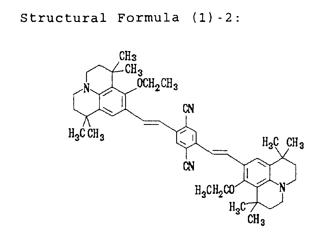
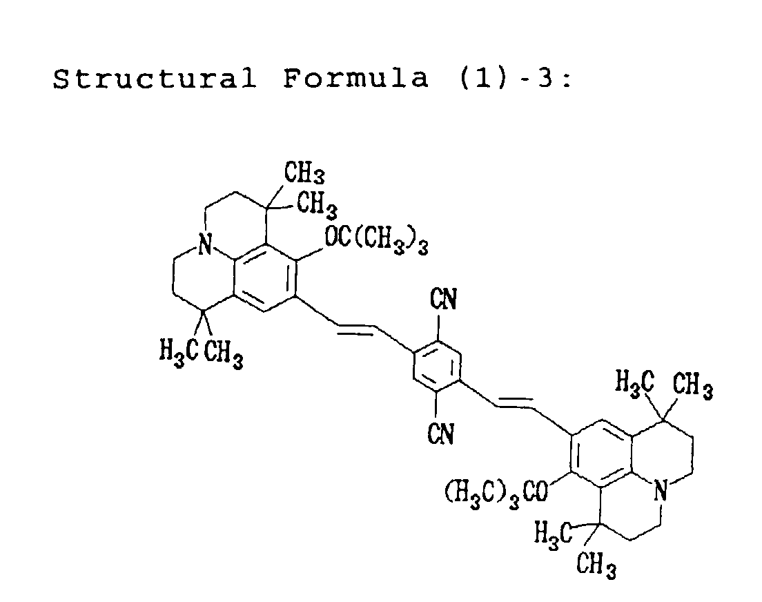
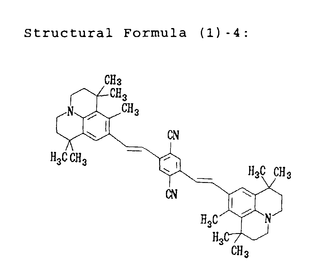
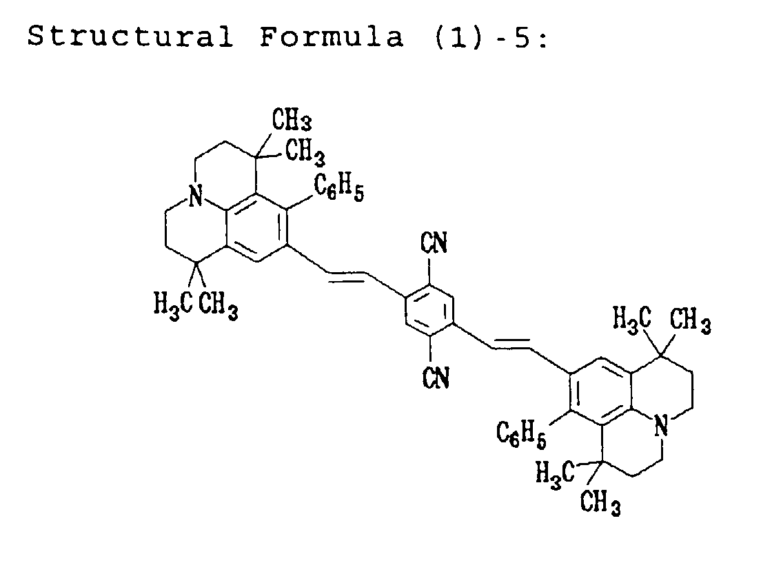
structural formula (1)-1, (1)-2, (1)-3, (1)-4, (1)-5,
(1)-6, (1)-7 or (1)-8.
-
Figs. 1 to 4, respectively, show examples of
organic electroluminescent devices according to the
invention, in which like reference numerals indicate like
parts or members, respectively.
-
Fig. 1 shows organic electroluminescent device A of
a transmission type in which luminescent light 20 passes
through a cathode 3, and the light 20 can also be
observed from a side of a protective layer 4. Fig. 2
shows organic electroluminescent device B of a reflection
type wherein light reflected at the cathode 3 can also be
obtained as luminescent light.
-
In the figures, reference numeral 1 indicates a
substrate for forming an organic electroluminescent
device, which may be made of glass, plastics and other
appropriate materials. Where the organic
electroluminescent device is used in combination with
other types of display devices, the substrate 1 may be
commonly used. Reference numeral 2 indicates a
transparent electrode (anode), for which ITO (indium tin
oxide), SnO2 or the like may be used.
-
Reference numeral 5 indicates an organic
luminescent layer, which contains the above-mentioned
julolidyl-substituted styryl compound as a luminescent
material. For a layer arrangement for obtaining organic
electroluminescence 20, the luminescent layer 5 may have
hitherto known various types of layer arrangements. As is
described hereinafter, if a material for either a hole
transport layer or an electron transport layer has
luminescent properties, for example, a built-up structure
of these thin films may be used. Further, in order to
increase charge transportability within a range
satisfying the purposes of the invention, either or both
of a hole transport layer and an electron transport layer
have a built-up structure of thin films made of plural
types of materials, or a thin film composed of a mixture
of plural types of materials may be used without
limitation. In addition, in order to improve luminescent
properties, at least one fluorescent material may be used
to provide a structure wherein the thin film of the
fluorescent material is sandwiched between the hole
transport layer and the electron transport layer.
Alternatively, another type of structure may be used
wherein at least one fluorescent material is present in
the hole transport layer or in the electron transport
layer, or in both of them. In these cases, in order to
improve a luminescent efficiency, a thin film for
controlling the transport of holes or electrons may be
incorporated in the layer arrangement.
-
The julolidyl-substituted styryl compound
represented by the structural formula (1) has both
electron transportability and hole transportability, and
can be used as a luminescent layer serving also as an
electron transport layer, or as a luminescent layer
serving as a hole transport layer in the device
arrangement. Moreover, it is possible to provide an
arrangement wherein the julolidyl-substituted styryl
compound is formed as the luminescent layer sandwiched
between the electron transport layer and the hole
transport layer.
-
It will be noted that in Figs. 1 and 2, reference
numeral 3 indicates a cathode, and an electrode material
may be made of an alloy of an active metal, such as Li,
Mg, Ca or the like, and a metal, such as Ag, Al, In or
the like, or a built-up structure of thin films of these
metals may also be used. In the transmission-type organic
electroluminescent device, the optical transmission
required for an intended application can be obtained by
controlling a cathode thickness. In the figures,
reference numeral 4 indicates a sealing/protective layer,
and when an organic electroluminescent device is wholly
covered therewith, its effect increases. Appropriate
materials may be used for this provided that air
tightness is ensured. Reference numeral 8 indicates a
drive power supply for current charge.
-
In the organic electroluminescent device of the
invention, the organic layer may have an organic built-up
structure (single hetero structure) wherein a hole
transport layer and an electron transport layer are built
up and wherein the above-mentioned julolidyl-substituted
styryl compound can be used as a material for forming the
hole transport layer or electron transport layer.
Alternatively, the organic layer may have an organic
built-up structure (double hetero structure) wherein a
hole transport layer, a luminescent layer and an electron
transport layer are successively built up, and the
luminescent layer can be formed of the above-mentioned
julolidyl-substituted styryl compound.
-
An example of the organic electroluminescent device
having such an organic built-up structure is shown. More
particularly, Fig. 3 shows an organic electroluminescent
device C having a single hetero structure which consists
of a built-up structure comprising, on an optically
transparent substrate 1, an optically transparent anode 2,
an organic layer 5a consisting of a hole transport layer
6 and an electron transport layer 7, and a cathode 3
superposed successively in this order, and the built-up
structure is sealed with the protective layer 4.
-
With such a layer arrangement as shown in Fig. 3
wherein a luminescent layer is omitted, luminescent light
20 with a given wavelength is emitted from the interface
between the hole transport layer 6 and the electron
transport layer 7. This light is observed from the side
of the substrate 1.
-
Fig. 4 shows an organic electroluminescent device D
having a double hetero structure which consists of a
built-up structure comprising, on an optically
transparent substrate 1, an optically transparent anode 2,
an organic layer 5b consisting of a hole transport layer
10, a luminescent layer 11 and an electron transport
layer 12, and a cathode 3 superposed successively in this
order. The built-up structure is sealed with a protective
layer 4.
-
In the organic electroluminescent device shown in
Fig. 4, when a DC voltage is applied between the anode 2
and the cathode 3, the holes injected from the anode 2
arrive at the luminescent layer 11 via the hole transport
layer 10, and the electrons injected from the anode 3
also arrive at the luminescent layer 11 via the electron
transport layer 12. Eventually, the electrons/the holes
are re-combined in the luminescent layer to generate
singlet excitons, thereby causing light with a given
wavelength to be generated from the singlet excitons.
-
In the above-stated organic electroluminescent
devices C and D, optically transparent materials such as,
for example, glass, plastics and the like may be
appropriately used as the substrate 1. Where the devices
are used in combination with other types of display
devices, or where the built-up structures shown in Figs.
3 and 4 are arranged in the form of a matrix, the
substrate may be commonly used. Both of the devices C and
D may have a structure of either a transmission type or a
reflection type.
-
The anode 2 consists of a transparent electrode,
for which ITO (indium tin oxide), SnO2 or the like may be
used. In order to improve a charge injection efficiency,
a thin film made of an organic material or an
organometallic compound may be provided between the anode
2 and the hole transport layer 6 (or the hole transport
layer 10). It will be noted that where the protective
layer 4 is formed of a conductive material such as a
metal, an insulating film may be provided at the sides of
the anode 2.
-
The organic layer 5a of the organic
electroluminescent device C consists of a built-up
organic layer of the hole transport layer 6 and the
electron transport layer 7, and the afore-indicated
julolidyl-substituted styryl compound may be contained in
either or both of these layers to provide a luminescent
hole transport layer 6 or electron transport layer 7. The
organic layer 5b of the organic electroluminescent device
D consists of a built-up organic layer of the hole
transport layer 10, the luminescent layer 11 containing
such a julolidyl-substituted styryl compound as set out
before, and the electron transport layer 12. The layer 5b
may take other various types of built-up structures. For
instance, either or both of the hole transport layer and
the electron transport layer may have luminescent
properties.
-
Especially, it is preferred that the hole transport
layer 6 or electron transport layer 7, and the
luminescent layer 11, respectively, consist of a layer
made of the julolidyl-substituted styryl compound used in
the present invention. These layers may be formed of the
afore-mentioned julolidyl-substituted styryl compound
alone, or may be formed through co-deposition of the
julolidyl-substituted styryl compound and other type of
hole or electron transport material (e.g., an aromatic
amine, a pyrazoline or the like). Moreover, in order to
improve the hole transportability in the hole transport
layer, a hole transport layer, which consists of a
plurality of hole transport materials being built up, may
be formed.
-
In the organic electroluminescent device C, the
luminescent layer may be the electron transport
luminescent layer 7. In this case, light may be emitted
from the hole transport layer 6 or its interface
depending on the voltage applied to from a power supply 8.
Likewise, in the organic electroluminescent device D, the
luminescent layer may be, aside from the layer 11, the
electron transport layer 12 or the hole transport layer
10. For improving the luminescent performance, it is
preferred to provide a structure wherein the luminescent
layer 11 containing at least one fluorescent material is
sandwiched between the hole transport layer and the
electron transport layer. Alternatively, a fluorescent
material may be contained in the hole transport layer or
the electron transport layer, or in both layers. In this
connection, in order to improve a luminescent efficiency,
a thin film (such as a hole blocking layer or an exciton-generating
layer) for controlling the transport of holes
or electrons may be provided in the layer arrangement.
-
The materials used as the cathode 3 may be alloys
of active metals such as Li, Mg, Ca and the like and
metals such as Ag, Al, In and the like, or a built-up
structure of the layers of these metals may also be used.
Proper selection in cathode thickness and in type of
alloy or metal enables one to fabricate an organic
electroluminescent device adapted for its application.
-
The protective layer 4 acts as a sealing film, and
is arranged to wholly cover an organic electroluminescent
device therewith, thereby ensuring an improved charge
injection efficiency and luminescent efficiency. It
should be noted that if air tightness is ensured, a
material including a single metal such as aluminium, gold,
chromium or the like, or an alloy thereof may be
appropriately selected for this purpose.
-
The an electric current applied to the respective
organic electroluminescent devices set out hereinabove is
usually a direct current, but a pulse current or AC
current may also be used. The values of current and
voltage are not critical provided that they are within
ranges not breaking the devices down. Nevertheless,
taking into account the power consumption and life of the
organic electroluminescent devices, it is preferred to
cause luminescence efficiently by use of an electric
energy which is as small as possible.
-
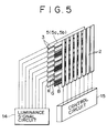
Next, Fig. 5 shows an arrangement of a flat display,
which makes use of an organic electroluminescent device
of the invention. As shown in the figure, with the case,
for example, of a full color display, organic layers 5
(Sa, 5b) capable of generating luminescent three primary
colors of red (R), green (G) and blue (B) are arranged
between cathodes 3 and anodes 2. The cathodes 3 and the
anodes 2 may be provided in the form of a stripe in which
they are mutually intersected, and are properly selected
by means of a luminance signal circuit 14 and a shift
register built-in control circuit 15 and applied with a
signal voltage thereto. As a result, an organic layer at
a position (picture element) where the selected cathode 3
and anode 2 are intersected emits light.
-
More particularly, Fig. 5 shows, for example, an 8
× 3 RGB simple matrix wherein the organic layer 5 as a
built-up body consisting of a hole transport layer and at
least one of a luminescent layer and an electron
transport layer is provided between the cathodes 3 and
the anodes 2 (see Fig. 3 or 4). The cathodes and anodes
are patternized in the form of a stripe and are mutually
intersected in a matrix, to which signal voltages are
applied in time series from the shift register built-in
control circuits 15 and 14, thereby causing
electroluminescence or light emission at the intersected
position. The EL device having such an arrangement may be
used not only as a display for letters/symbols, but also
as an image reproducing apparatus. Moreover, the striped
patterns of the anodes 3 and the cathodes 2 may be
arranged for each of red (R), green (G) and blue (B)
colors, thus making it possible to fabricate a solid-state
flat panel display of the multicolor or full color
type.
-
For the preparation of the julolidyl-substituted
styryl compound in a high efficiency, a formylated
julolidyl compound of the general formula [III] or [IV]
are reacted with a diphosphonic acid ester of the
following general formula [V] or a diphosphonium compound
of the following general formula [VI], thereby obtaining
the julolidyl-substituted styryl compound of the afore-indicated
general formula [I] or [II]:
wherein X
3 represents a hydrogen atom, a hydroxyl group,
an alkoxyl group, an alkyl group, an amino group, an
alkylamino group, or a substituted or unsubstituted aryl
group corresponding to X
1 and X
2 defined before,
respectively, R
13, R
14, R
15 and R
16, respectively, represent
a lower alkyl group corresponding to R
1, R
2, R
3, R
4, R
5, R
6,
R
7 and R
8 defined before and may be the same or different;
wherein R
17 and R
18 may be the same or different and
independently represent a hydrocarbon group, R
19, R
20, R
21
and R
22, respectively, represent an electron attracting
group corresponding to R
9, R
10, R
11 and R
12 defined before
and may be the same or different, and Y represents a
halogen atom such as a chlorine atom.
-
More specifically, in the method of preparing the
julolidyl-substituted styryl compound, the reaction
(condensation) is carried out by the Wittig-Horner
reaction or the Wittig reaction wherein the diphosphonic
acid ester and/or the diphosphonium compound is treated
with a base in a solvent to form a carbanion, and the
carbanion is condensed with the formylated julolidyl
compound.
-
The reaction scheme of the condensation reaction
can be shown, for example, by the following
Reaction
Scheme 1 or 1'.
-
This reaction starts with the formation of a
carbanion by treating the compound of the general formula
(1) or (2) with a base in an appropriate solvent, and
completes with the condensation of the carbanion with an
aldehyde of the general formula [III] or [IV]. The
combinations of a base and a solvent are considered to be
ones including sodium hydroxide/water, sodium
carbonate/water, potassium carbonate/water, sodium
ethoxide/ethanol or dimethylformamide, sodium
methoxide/methanol-diethyl ether mixed solvent or
dimethylformamide, triethylamine/ethanol, diglyme,
chloroform or nitromethane, pyridine/methylene chloride
or nitromethane, 1,5-diazabicyclo[4.3.0]non-5-en/dimethylsulfoxide,
potassium t-butoxide/dimethyl
sulfoxide or tetrahydrofuran, butyl lithium/diethyl ether,
tetrahydrofuran, benzene or dimethylformamide, phenyl
lithium/diethyl ether or tetrahydrofuran, sodium
amide/ammonia, sodium hydride/dimethylformamide or
tetrahydrofuran, trityl sodium/diethyl ether or
tetrahydrofuran, and the like.
-
The reaction proceeds at a relatively low
temperature of -30°C to 30°C and is selective, so that
the purification of an intended product through
chromatography is easy. In addition, the compound of the
general formula [I'] or [II'] is so high in crystallinity
that the purity can be improved via re-crystallization.
The re-crystallization method is not critical, and is
simply feasible according a method of dissolving the
product in acetone and adding hexane to the solution,
with subsequent removal of the solvents by distillation
being easy. This reaction may be performed under
conditions of a normal temperature to 30°C, a normal
pressure and 1 to 24 hours.
-
It is preferred that the reaction is caused to
proceed according to the following reaction formulae to
obtain the julolidyl-substituted styryl compound of the
following general formula [I'] or [II']:
In the general formulae [I'], [I"], [III'] and [III"], R
1,
R
2, R
3, R
4, R
5, R
6, R
7, R
8, R
9, R
10, R
11, R
12, R
13, R
14, R
15 and
R
16, respectively, have the same meanings as defined
before, R
23 represents an alkyl group preferably having 1
to 6 carbon atoms such as a methyl group, an ethyl group
or the like, or an alkoxyalkyl group preferably having 2
to 6 carbon atoms such as a methoxymethyl group or the
like, and X
4 represents a halogen atom such as, for
example, a chlorine atom, an iodine atom or the like.
-
The reaction is more particularly shown below:
-
It is preferred that the reaction for obtaining the
compound of the general formula [I'] from the compound of
the general formula [III'] is conducted according to the
Wittig-Horner reaction or the Wittig reaction wherein the
diphosphonic acid ester and/or the diphosphonium compound
is treated with a base in a solvent thereby forming a
carbanion. The thus formed carbanion is condensed with
the compound of the general formula [III'], and the
compound of the general formula [I'] obtained through the
condensation is hydrolyzed with a strong acid such as HCl
to obtain the compound of the general formula [I"].
-
In the above reactions, the hydroxyl group (OH) of
the compound of the general formula [III'] is protected
through etherification with an alkyl group or the like
(R23), under which the Wittig-Horner reaction or Wittig
reaction is carried out, and the ether moiety is finally
hydrolyzed. Thus, the compound of the general formula
[I"] can be reliably synthesized in high yield. If R23 =
CH2OCH3, the hydrolysis proceeds readily.
-
It will be noted that the formylated julolidyl
compound of the following general formula [IV], which is
a synthetic intermediate of the julolidyl-substituted
styryl compound, is a novel compound
wherein R
13, R
14, R
15 and R
16, respectively have the same
meanings as defined before.
-
This synthetic intermediate can be prepared from
its precursor in the following manner.
-
More particularly, the julolidyl compound of the
general formula [VII] is formylated by means of an adduct
of dimethylformamide and a halogenated phosphoryl
compound to obtain the formylated julolidyl compound of
the general formula [IV]. This formylation reaction can
be carried out in dimethylformamide at a temperature of
room temperature (20°C) to 80°C at a normal pressure for
2 to 24 hours
wherein R
13, R
14, R
15 and R
16, respectively have the same
meanings as defined before.
-
In this case, it is preferred that aniline or an m-substituted
aniline of the following general formula and
a 1-halogenated-3,3-dialkyl-2-propene are reacted with
each other, and the resultant 3-[N,N-bis(3,3-dialkyl-2-[propenyl]amine
salt is further reacted with a
alkylsulfonic acid. The resulting 1,1,7,7-tetraalkyljulolidine
alkylsulfonate is neutralized with
an alkali, followed by formylation of the resultant
1,1,7,7-tetraalkyljulolidine
wherein R represents a hydrocarbon group, a halogen atom,
an alkoxyl group or the like.
-
The compound (1) or (2) serving as the synthetic
intermediate can be derived from a synthetic intermediate
used as its precursor in the following manner.
-
The halogenated aryl compound of the following
general formula [VIII] and an trialkyl phosphite of the
following general formula [IX] or triphenylphosphine
(PPh
3) are reacted with each other, to obtain, as a
synthetic intermediate, a diphosphonic acid ester or
diphosphonium of the afore-indicated general formula (1)
or (2). This reaction is effected in a solvent-free
condition, in an excess of the trialkyl phosphite or in a
solvent such as xylene or the like at a reaction
temperature of 120 to 160°C at a normal pressure for a
reaction time of 30 minutes to 12 hours:
wherein Z represents a halogen atom; and
General Formula [IX]:
P(OR24)3 or P(OR25)3
wherein R
24 and R
25 may be the same or different and
independently represent a hydrocarbon group, preferably a
saturated or unsaturated hydrocarbon group having from 1
to 4 carbon atoms and correspond to R
17 or R
18,
respectively.
-
The
above scheme 1 or 1' is more particularly
described in the order of the following steps (a) to (e).
- (a) 2,5-Dimethylterephthalonitrile is brominated to
prepare 2,5-diboromomethylterephthalonitrile.
- (b) This compound is reacted with triethyl
phosphite under reflux to prepare a diphosphonic acid
ester (1).
- (c) On the other hand, aniline or an m-substituted
aniline is mixed with N,N-dimethylformamide or calcium
carbonate, to which a 1-chloro-3,3-dialkyl-2-propene is
added at 80°C or below, followed by gentle addition of
water to permit a 3-[N,N-bis(3,3-dialkyl-2-propenyl)amine
hydrochloride salt to be precipitated.
- (d) The salt is reacted with an alkylsulfonic acid
to obtain a 1,1,7,7-tetraalkyljulolidine alkylsulfonate.
This salt is neutralized with sodium hydroxide. The
resultant 1,1,7,7-tetraalkyljulolidine is reacted with a
phosphoryl chloride solution in N,N-dimethylformamide
(DMF) to obtain, as a major product, 1,1,7,7-tetraalkyljulolidine-9-carbaldehyde
[III] and, as a minor
product, 1,1,7,7-tetraalkyljulolidine-6-carbaldehyde [IV].
- (e) Next, the 1,1,7,7-tetraalkyljulolidine-9-carbaldehyde
[III] (including one which undergoes an
alkoxy substitution at the 8 position) or 1,1,7,7-tetraalkyljulolidine-8-carbaldehyde
[IV] and the
phosphoric acid ester (1) are subjected to the Wittig-Horner
reaction (i.e., treated with sodium hydride in
tetrahydrofuran), thereby obtaining an intended
julolidyl-substituted styryl compound [I'].
-
-
The invention is more particularly described by way
of examples, which should not be construed as limiting
the invention thereto.
-
Synthetic intermediates, which are used to prepare
a julolidyl-substituted styryl compound employed to make
an organic electroluminescent device, were prepared in a
manner as exemplified below.
2,5-Dibromomethylterephthalonitrile (3)
-
-
3.02 g (20 mmol) of 2,5-dimethylterephthalonitrile
in 100 ml of benzene was refluxed at 100°C along with
35.50 g (100 mmol) of N-bromosuccinimide until the
reaction was completed. The re-crystallization from
acetone/hexane resulted in 2.00 g (yield: 33%) of a pure
product (3) as a light white solid.
-
The analytical data of this product are shown below.
1H NMR (400 MHz, CDCl3) : δ 4.6 ppm (s, 4H, 2CH2), 7.9 ppm
(s, 2H, aromatics)
Diphosphonic acid ester (1)
-
-
1.20 g (3.8 mmol) of the above 2, 5-dibromomethylterephthalonitrile
(3) was refluxed at 125°C
for 2 hours along with 5 ml of triethyl phosphite. The
excess triethyl phosphite was removed under reduced
pressure. The diphosphonic acid ester (1) was obtained as
light yellow crystals through re-crystallization from
acetone/hexane.
-
The analytical data of this product are shown below.
1H NMR (400 MHz, CDCl3): δ 1.2 ppm (t, 12H, 4CH3), 3.2 ppm
(d, 4H, 2CH2), 4.1 ppm (m, 8H, 4CH2), 7.9 ppm (s, 2H,
aromatics)
8-Hydroxy-1,1,7,7-tetraalkyl (e.g. methyl)julolidine-9-carbaldehyde
(4)
-
-
This aldehyde reagent (4) is commercially available
based on Acros Organics Catalogue of Fine Chemicals and
was used without purification.
8-Alkoxy (e.g. methoxy)-1,1,7,7-tetralkyl (e.g.
methyl)julolidine-9-carbaladehyde (5a)
-
-
3.00 g (11.0 mmol) of 8-hydroxy-1,1,7,7-tetramethyljulolidine-9-carbaldehyde
and 15.2 g (110
mmol) of potassium carbonate were suspended in 300 ml of
acetone and refluxed. 10.4 g (73.2 mmol) of methyl iodide
was added to the suspension in every 90 minutes after
division into four portions, followed by refluxing for 12
hours.
-
The reaction solution was cooled down to room
temperature, and the resultant insoluble matter was
removed by filtration. The filtrate was concentrated, and
isolated for purification through silica gel
chromatography (Wakogel C-300, tetrahydrofuran : hexane =
1 : 2). The resultant eluate was concentrated and
recrystallized from acetone-hexane to obtain 2.98 g
(yield: 94%) of 8-methoxy-1,1,7,7-tetramethyljulolidine-9-carbaldehyde
(5a).
-
The analytical data of this product are shown below.
1H NMR (270 MHz, CDCl3): δ 1.3 and 1.4 ppm (s, 6H, CH3),
1.7 ppm (m, 2H, CH2), 3.3 ppm (m, 2H, CH2), 3.9 ppm (s, 3H,
OCH3), 7.5 ppm (s, H, aromatic), 10.0 ppm (s, 1H, CHO)
8-Methoxymethoxy-1,1,7,7-tetramethyljulolidine-9-carbaldehyde
(5b)
-
-
52.2 mmol of sodium hydride (60% mineral oil
dispersion) was washed twice with a small amount of
hexane in an atmosphere of nitrogen, and suspended in 20
ml of dry tetrahydrofuran. A solution of 2.00 g (7.31
mmol) of 8-hydroxy-1,1,7,7-tetramethyljulolidine-9-carbaldehyde
(4) dissolved in 20 ml of dry
tetrahydrofuran was dropped at 0°C, followed by agitation
for 30 minutes as it is. 4.23 g (52.5 mmol) of
methoxymethyl chloride was further added to, followed by
agitation at room temperature for 4 hours.
-
The reaction solution was quenched with a small
amount of ice pieces on an ice bath, washed with a
saturated saline solution and dried over sodium sulfate.
8-methoxymethoxy-1,1,7,7-tetramethyljulolidine-9-carbaldehyde
(5b) was obtained at a yield of 50% by
isolation through silica gel chromatography (Wakogel C-200,
tetrahydrofuran).
-
The analytical data of this product are shown below.
1H NMR (270 MHz, DMSO-d6): δ 1.4 ppm (s, 6H, CH3), 1.7 ppm
(m, 2H, CH2), 3.3 ppm (m, 2H, CH2), 3.5 ppm (s, 3H, OCH3),
5.0 ppm (s, 2H, CH2O), 7.4 ppm (s, H, aromatic), 9.7 ppm
(s, 1H, CHO)
1,1,7,7-Tetramethyljulolidine-9-carbaldehyde (6)
-
(a) 3-[N,N-bis(3-methyl-2-buten-1-yl)aminophenyl
hydrochloride
-
100 ml of DMF (dimethylformamide), 23.28 g (0.25
mol) of aniline and 12.5 g (0.125 mol) of calcium
carbonate were charged into a 500 ml round bottom flask
equipped with a nitrogen introducing pipe, a mechanical
stirrer and a 50 ml dropping funnel having a condenser.
The resultant mixture was heated to 65°C, to which 53.59
g (0.5 mol) of 1-chloro-methylbutene was fed from the
dropping funnel. This alkene was added to while strongly
stirring over 15 minutes at a temperature kept at 80°C or
below, followed by further agitation at 80'C for 40
minutes and cooling down to room temperature by immersion
in an ice bath.
-
While strongly stirring, 100 ml of water was gently
added to, followed by passage through a glass filter to
remove the resultant precipitate by filtration. The
filter cake was washed with diethyl ether (2 × 40 ml) and
dried for 1 hour under suction, followed by further
washing with 40 ml of diethyl ether and suction drying at
50°C for 3 hours. As a result, 30.35 g (yield: 46%) of 3-[N,N-bis(3-methyl-2-buten-1-yl)]aminophenyl
hydrochloride
as a white solid powder product.
-
The analytical data of the product are shown below.
1H NMR (270 MHz, CDCl3): δ 1.4 and 1.6 ppm (s, 6H, 2CH3),
3.9 ppm (s, 4H, 2CH2), 5.4 ppm (m, 2H, CH=C), 7.3 - 7.7
ppm (m, 5H, aromatics)
(b) Methylsulfonate of 1,1,7,7-tetramethyljulolidine
-
25 ml of methanesulfonic acid was charged into a
300 ml round bottom flask equipped with a nitrogen
introducing pipe, a mechanical stirrer and a funnel for
powder. 20.2 g of the solid 3-[N,N-bis(3-methyl-2-buten-1-yl)]aminophenyl
hydrochloride was added to the acid
under strong agitation in 25 minutes. The reaction
mixture was heated to 100°C, at which it was maintained
for 1 hour. Thereafter, the cooled down to 40°C on an ice
bath, after which it was slowly poured into 100 ml of
strongly agitated, ice-cooled water in 15 minutes,
followed by extraction with CHCl3 (3 × 100 ml).
-
The organic phase was dried over MgSO4 (magnesium
sulfate) and filtered, followed by removal of the solvent
with a rotary evaporator to obtain the product
(methylsulfonate of 1,1,7,7-tetramethyljulolidine) as a
viscous brown oil at a quantitative yield.
-
The analytical data of this product are shown below.
1H NMR (270 MHz, CDCl3) : δ 1.1 - 1.9 ppm (m, 12H, 4CH3),
0.9 - 1.9 ppm (m, 4H, 2CH2), 2.6 - 2.8 ppm (m, 4H, 2CH2),
7.2 - 7.8 ppm (m, 3H, aromatics)
(c) 1,1,7,7-Tetramethyljulolidine
-
29 g (90 mmol) of the 1,1,7,7-tetramethyljulolidine
methylsulfonate was slowly added to
50 ml of an aqueous solution of 4.04 g (100 mmol) of
sodium hydroxide, strongly agitated. After agitation for
5 minutes, 100 ml of ethyl acetate was added to the
mixture, followed by agitation for 30 minutes.
-
The organic phase was dried over MgSO4 and
decolored, followed by filtration and evaporating with a
rotary evaporator to obtain 14.5 g (yield: 71%) of a
product (1,1,7,7-tetramethyljulolidine) in the form of a
brown oily substance.
-
The analytical data of this product are shown below.
1H NMR (270 MHz, CDCl3): δ 1.7 ppm (d, 12H, 4CH3), 2.1 ppm
(m, 4H, 2CH2), 3.4 - 3.9 ppm (m, 4H, 2CH2), 6.5 - 7.3 ppm
(m, 3H, aromatics)
(d) 1,1,7,7-Tetramethyljulolidine-9-carbaldehyde
-
7 ml of phosphoryl chloride was gently added to 20 ml
of N,N-dimethylformamide (DMF) cooled on an ice bath. The
resultant light yellow solution was agitated at room
temperature for 1 hour. The 1,1,7,7-tetramethyljulolidine
obtained above was dropped in the solution in 30 minutes,
during which the reaction mixture was changed to a dark
red. This mixture was heated to 65°C, at which it was
maintained for 3 hours, followed by pouring into strongly
agitated water.
-
The resulting dark rubbery matter was extracted
twice with 150 ml of hexane/ethyl acetate (1 : 1 mixture)
and dried over MgSO4 (magnesium sulfate), and the solvent
was removed in a rotary evaporator. The product was
purified via column chromatography (silica gel,
dichloromethane), followed by extraction with
hexane/ethyl acetate (6 : 1) to obtain a major product
(1,1,7,7-tetramethyljulolidine-9-carbaldehyde (6)) at a
yield of 54% in the form of an oily substance.
-
The analytical data of this product are shown below.
1H NMR (270 MHz, CDCl3): δ 1.15, 1.2, 1.25 and 1.3 ppm (s,
3H, 4CH3), 1.6 - 1.8 ppm (m, 4H, 2CH2), 3.7 ppm (m, 4H,
2CH2), 6.6 and 7.8 ppm (d, 1H, aromatics), 9.6 ppm (s, 1H,
CHO)
-
Along with the above product, there was obtained,
as a minor product, 1,1,7,7-tetramethyljulolidine-8-carbaldehyde
(7) of the following formula at a yield of
20%.
-
The analytical data of this minor product are shown
below.
1H NMR (270 MHz, CDCl3): δ 1.6 and 1.7 ppm (s, 6H, 2CH3),
1.5 - 2.2 ppm (m, 4H, 2CH2), 3.2 - 3.8 ppm (m, 4H, 2CH2),
7.7 and 6.9 ppm (m, 1H, aromatics), 9.7 ppm (s, 1H, CHO)
-
A preparatory example of a julolidyl-substituted
styryl compound is now described.
-
In particular, this reaction is expressed according
to the following reaction sequence:
-
In a typical procedure, 794 mg (4.78 mmol) of
triethyl phosphite was dropped in 750 mg (2.39 mmol) of
2,5-di(bromomethyl)terephthalonitrile, followed by
agitation at 125°C for 30 minutes to obtain diphosphonic
acid ester (1). Instead, where it was intended to use
diphosphonium (2), 750 mg (2.39 mmol) of 2,5-di(bromomethyl)-terephthalonitrile
and 1.38 g (5.26 mmol)
of triphenylphosphine were dissolved in xylene, followed
by refluxing for 20 hours to obtain diphosphonium (2).
-
On the other hand, 1.23 g (53 mmol, dispersed in an
oil at 60%) was charged into a 300 ml three-necked round
bottom flask equipped with a nitrogen introducing pipe
and a dropping funnel and having a magnetic stirrer, and
was washed three times with dry pentane under vigorous
agitation. Immediately after removal of an oily substance,
sodium hydride was suspended in 20 ml of dry THF
(tetrahydrofuran).
-
Thereafter, 4.95 mmol of diphosphonic acid ester
(1) or diphosphonium (2) in 50 ml of dry THF was added
slowly to the reaction mixture in 1 hour. The reaction
mixture was agitated for further 1 hour, in which 10 mmol
of each of the aldehydes (4), (5a), (5b), (6) and (7) in
50 ml of THF was dropped, for example.
-
The reaction mixture was isolated through
chromatography and subsequently quenched with 1 ml of ice.
Thus cooled reaction mixture was poured into a 5% sodium
bicarbonate aqueous solution, extracted with
dichloromethane (3 × 50 ml), washed with a saline
solution (1 × 20 ml) and dried over anhydrous sodium
sulfate. The solvent was removed by a rotary evaporator,
followed by purification of the product (8), (9a), (9b),
(10) or (11) through column chromatography (SiO2,
THF/hexane) and re-crystallization from acetone/hexane.
-
In another procedure, 7.72 mmol of sodium hydride
(60% dispersion in a mineral oil) was washed twice with a
small amount of hexane in an atmosphere of nitrogen,
suspended in 5 ml of dry tetrahydrofuran, and cooled down
to -78°C. A solution of phosphonic acid ester (1) in an
amount corresponding to 1.93 mmol and 1.49 g (5.18 mmol)
of 8-methoxy-1,1,7,7-tetramethyljulolidine-9-carbaldehyde
(5a) dissolved in 60 ml of tetrahydrofuran was dropped in
the suspension, after which the temperature of the
mixture was raised and agitated at room temperature for 1
hour.
-
The reaction solution was quenched with a small
amount of ice, washed with a saturated saline solution
and dried over sodium sulfate. Silica chromatography
(Wakogel C-300, tetrahydrofuran : hexane = 1 : 8) was
used for isolation and purification, followed by re-crystallization
from acetone-hexane and repeated washings
of the resultant precipitate with ethanol to obtain 813
mg (yield: 61%) of the julolidyl-substituted styryl
compound (9a).
-
Moreover, 10.4 mmol of sodium hydride (60%
dispersion in a mineral oil) was washed twice with a
small amount of hexane in an atmosphere of nitrogen,
suspended in 10 ml of dry tetrahydrofuran, and dropped in
25 ml of a dry tetrahydrofuran solution of phosphoric
acid ester (1) in an amount corresponding to 1.73 mmol at
0°C, followed by agitation for 5 minutes. A solution of
2.5 mmol of 8-methoxymethoxy-1,1,7,7-tetramethyljulolidine-9-carbaldehyde
(5b) dissolved in 40
ml of tetrahydrofuran was dropped at 0°C, and was raised
in temperature and agitated at room temperature for
further 1 hour.
-
The reaction solution was quenched with a small
amount of ice, washed with a saturated saline solution
and dried over sodium sulfate. Silica chromatography
(Wakogel C-300, toluene : hexane = 1 : 1 →
tetrahydrofuran : hexane = 1 : 1) was used for isolation
and purification, followed by re-crystallization from
toluene-ethanol and repeated washings of the resultant
precipitate with ethanol (EtOH) to obtain 309 mg (yield:
24%) of the julolidyl-substituted styryl compound (9b).
-
Further, 76.3 mg (0.101 mmol) of julolidyl-substituted
styryl compound (9b) was dissolved in 15 ml
of chloroform, to which 0.5 ml of concentrated
hydrochloric acid and 2 ml of ethanol were added,
followed by heating and agitation at 50°C for 4 hours.
The reaction solution was cooled, to which 20 ml of a
potassium carbonate aqueous solution was added for
neutralization. The resultant insoluble component was
removed by filtration and extracted with tetrahydrofuran,
followed by washing with a diluted hydrochloric acid
solution and then with a saturated saline solution and
drying over sodium sulfate. Silica gel chromatography
(Wakogel C-300, toluene) was used for isolation and
purification, followed by re-crystallization from toluene
to obtain 5 mg (yield: 67%) of julolidyl-substituted
styryl compound (8).
Product (9a) or compound of structural formula (1)-1
(wherein X1 = X2 = OCH3)
-
This product (9a) was obtained, as shown in the
afore-indicated reaction scheme, through reaction between
8-methoxy-1,1,7,7-tetramethyljulolidine-9-carbaldehyde
(5a) and diphosphonic acid ester (1).
-
The analytical data of this product are shown below.
FAB-MS: m/e = 695
1H NMR (270 MHz, CDCl3): δ 1.3 and 1.6 ppm (s, 12H, CH3),
1.8 ppm (m, 4H, CH2), 3.2 ppm (m, 4H, CH2), 3.8 ppm (s, 6H,
OCH3), 7.0 ppm (s, 2H, aromatic), 7.1 ppm (d, 2H, CH=),
7.4 ppm (d, 2H, CH=), 8.0 ppm (s, 2H, aromatic)
-
The 1H NMR spectrum is shown in Fig. 6 wherein the
abbreviation "TMS" means tetramethylsilane as a reference
herein and whenever it appears hereinafter.
UV-visible absorption spectrum (UV-Vis) (CHCl3): λmax =
508 nm
Photoluminescent spectrum (PL) (CHCl3) = PLmax = 600 nm (ex.
λ = 508 nm)
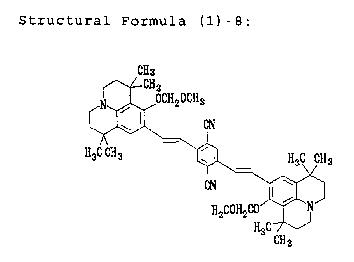
Product (9b) or compound of structural formula (1)-8 (X1 =
X2 = OCH2OCH3)
-
This product (9b) is, as shown in the afore-indicated
reaction scheme, obtained through reaction
between 8-methoxymethoxy-1,1,7,7-tetramethyljulolidine-9-carbaldehyde
(5b) and diphosphonic acid ester (1).
-
The analytical data of this product are shown below.
FAB-MS: m/e = 755
1H NMR (270 MHz, CDCl3): δ 1.3 and 1.5 ppm (s, 12H, CH3),
1.7 ppm (m, 4H, CH2), 3.2 ppm (m, 4H, CH2), 3.7 ppm (s, 6H,
CH3O), 5.0 ppm (s, 4H, CH2O), 7.1 ppm (d, 2H, CH=), 7.4
ppm (s, 2H, aromatic), 7.6 ppm (d, 2H, CH=), 8.0 ppm (s,
2H, aromatic)
-
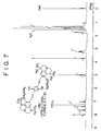
The 1H NMR spectrum is shown in Fig. 7.
UV-visible absorption spectrum (UV-Vis) (CHCl3): λmax =
505 nm
Photoluminescent spectrum (PL) (CHCl3) = PLmax = 590 nm (ex.
λ = 505 nm)
Product (8) or compound of structural formula (1)-6 (X1 =
X2 = OH)
-
This product (8) is, as shown in the afore-indicated
reaction scheme, obtained through hydrolysis of
8-methoxymethoxy-1,1,7,7-tetramethyljulolidine-9-carbaldehyde
(9b).
-
The analytical data of this product are shown below.
FAB-MS: m/e = 667
1H NMR (270 MHz, CDCl3): δ 1.3 and 1.5 ppm (s, 12H, CH3),
1.8 ppm (m, 4H, CH2), 3.4 ppm (m, 4H, CH2), 5.1 ppm (s, 2H,
OH), 7.1 ppm (d, 2H, CH=), 7.3 ppm (s, 2H, aromatics),
7.5 ppm (d, 2H, CH=), 7.9 ppm (s, 2H, aromatics)
-
The 1H NMR spectrum is shown in Fig. 8.
UV-visible absorption spectrum (UV-Vis) (CHCl3): λmax =
509 nm
Photoluminescent spectrum (PL) (CHCl3) = PLmax = 610 nm (ex.
λ = 509 nm)
Product (10) (X1 = X2 = H)
-
This product (10) is, as shown in the afore-indicated
reaction scheme, obtained through reaction
between 1,1,7,7-tetramethyljulolidine-9-carbaldehyde (6)
and diphosphonic acid ester (1).
-
The analytical data of this product are shown below.
TOF-MASS spectrum (time of flight mass spectrum): m/e 634
(m+)
1H NMR (400 MHz, CDCl3): δ 1.5 and 1.6 ppm (s, 12H, 4CH3),
1.8 - 2.0 ppm (m, 8H, 4CH2), 2.8 ppm (m, 8H, 4CH2), 8.0 -
6.9 ppm (m, 10H, aromatics and 2CH=CH)
Absorption spectrum by UV-visible light spectroscopy (UV-Vis)
(CHCl3): λmax = 481 nm
Photoluminescent spectrum (PL) (CHCl3) = PLmax = 590 nm (ex.
λ = 481 nm)
Product (11)
-
This product (11) is, as shown in the afore-indicated
reaction scheme, obtained through reaction
between 1,1,7,7-tetramethyljulolidine-8-carbaldehyde (7)
and diphosphonic acid ester (1).
-
The analytical data of this product are shown below.
TOF-MASS spectrum (time of flight mass spectrum): m/e 634
(m+)
1H NMR (400 MHz, CDCl3): δ 1.0 and 1.5 ppm (s, 12H, 4CH3),
1.5 - 2.2 ppm (m, 8H, 4CH2), 3.7 ppm (m, 8H, 4CH2), 8.8 -
6.8 ppm (m, 10H, aromatics and 2CH-CH)
Absorption spectrum by UV-visible light spectroscopy (UV-Vis)
(CHCl3): λmax = 474 nm
Photoluminescent spectrum (PL) (CHCl3) = PLmax = 590 nm (ex.
λ = 474 nm)
Optical properties of the respective products
-
The optical properties of the products shown above
are summarized in the following table.
| Product | UV-Vis (CHCl3) | PL (CHCl3) |
| (9a) (X1 = X2 = OCH3) | 508 nm | 600 nm |
| (9b) (X1 = X2 = OCH2OCH3) | 505 nm | 590 nm |
| (8) (X1 = X2 = OH) | 509 nm | 610 nm |
| (10) (X1 = X2 = H) | 481 nm | 590 nm |
| (11) | 474 nm | 590 nm |
-
From these results, it will be seen that the
julolidyl-substituted styryl compounds are able to emit
intense luminescence, and are suitable for use as green
to red light-emitting materials in an organic
electroluminescent device.
-
Examples of fabricating an organic
electroluminescent device using the julolidyl-substituted
styryl compounds are shown.
Example 1
-
This example illustrates fabrication of an organic
electroluminescent device having a single hetero
structure using, as a hole transport luminescent material,
a compound of the following structural formula (1)-1,
which is a julolidyl-substituted styryl compound of the
general formula [I] wherein R
9 and R
11, respectively,
represent a cyano group and X
1 and X
2, respectively,
represent a methoxy group.
-
A 30 mm × 30 mm glass substrate, which had been
formed with a 100 nm thick anode made of ITO on one
surface thereof, was set in a vacuum deposition apparatus.
A metallic mask having a plurality of 2.0 mm × 2.0 mm
unit openings was placed, as a deposition mask, closely
to the substrate. The compound of the above structural
formula (1)-1 was subjected to vacuum deposition at a
vacuum of 10-4 Pa or below to form, for example, a 50 nm
thick hole transport layer (serving also as a luminescent
layer). The deposition rate was at 0.1 nm/second.
-
Further, Alq
3 (tris(8-quinolinol)aluminium) of the
following structural formula was provided as an electron
transport material and was deposited in contact with the
hole transport layer. The electron transport layer made
of Alq
3 was set at a thickness, for example, of 50 nm, and
the deposition rate was at 0.2 nm/second.
-
A built-up film of Mg and Ag provided as a cathode
material was used. To this end, Mg and Ag were,
respectively, deposited at a deposition rate of 1
nm/second to form, for example, a 50 nm thick Mg film and
a 150 nm thick Ag film. In this way, an organic
electroluminescent device as shown in Fig. 3 was
fabricated in Example 1.
-
Luminescent characteristics of the device were
evaluated by applying a forward bias DC voltage to the
thus fabricated organic electroluminescent device of
Example 1 in an atmosphere of nitrogen. The luminescent
color was red, and the device was then subjected to
spectral measurement, with the result that, as shown in
Fig. 9, a spectrum having a luminescent peak at 650 nm
was obtained. The spectral measurement was performed by
use of a spectroscope made by Otsuka Electronic Co., Ltd.
and using a photodiode array as a detector. Moreover,
when the device was subjected to voltage-luminance
measurement, there could be obtained a luminance of 1,000
cd/m2 at 8 V as is particularly shown in Fig. 10.
-
After the fabrication of the organic
electroluminescent device, the device was allowed to
stand over one month in an atmosphere of nitrogen, no
device degradation was observed. In addition, when the
device was subjected to forced degradation wherein
continuous light emission was carried out at an initial
luminance of 300 cd/m2 while keeping an electric current
at a given level. As a consequence, it took 600 hours
before the luminance was reduced to half.
Example 2
-
This example illustrates fabrication of an organic
electroluminescent device having a single hetero
structure using, as an electron transport luminescent
material, a compound of the structural formula (1)-1,
which is a julolidyl-substituted styryl compound of the
general formula [I] wherein R9 and R11, respectively,
represent a cyano group and X1 and X2, respectively,
represent a methoxy group.
-
A 30 mm × 30 mm glass substrate, which had been
formed with a 100 nm thick anode made of ITO on one
surface thereof, was set in a vacuum deposition apparatus.
A metallic mask having a plurality of 2.0 mm × 2.0 mm
unit openings was placed, as a deposition mask, closely
to the substrate. α-NPD (α-naphthylphenyldiamine) of
the following structural formula was subjected to vacuum
deposition at a vacuum of 10
-4 Pa or below to form, for
example, a 50 nm thick hole transport layer. The
deposition rate was at 0.1 nm/second.
-
Further, the compound of the structural formula
(1)-1 used as an electron transport material was vacuum
deposited in contact with the hole transport layer. The
thickness of the electron transport layer (serving also
as a luminescent layer) composed of the compound of the
structural formula (1)-1 was set, for example, at 50 nm,
and the deposition rate was at 0.2 nm/second.
-
A built-up film of Mg and Ag provided as a cathode
material was used. More particularly, Mg and Ag were,
respectively, deposited at a deposition rate of 1
nm/second to form, for example, a 50 nm thick Mg film and
a 150 nm thick Ag film. In this way, an organic
electroluminescent device of Example 2 as shown in Fig. 3
was fabricated.
-
Luminescent characteristics were evaluated by
applying a forward bias DC voltage to the thus fabricated
organic electroluminescent device of Example 2 in an
atmosphere of nitrogen. The luminescent color was red,
and the device was then subjected to spectral measurement
as in Example 1, with the result that, as shown in Fig.
11, a spectrum having a luminescent peak at 650 nm was
obtained. Moreover, when the device was subjected to
voltage-luminance measurement, there could be obtained a
luminance of 1,100 cd/m2 at 8 V as is particularly shown
in Fig. 12.
-
After the fabrication of the organic
electroluminescent device, the device was allowed to
stand over one month in an atmosphere of nitrogen, no
degradation of the device was observed. In addition, when
the device was subjected to forced degradation wherein
continuous light emission was carried out at an initial
luminance of 300 cd/m2 while keeping an electric current
at a given level. As a consequence, it took 550 hours
before the luminance was reduced to half.
Example 3
-
This example illustrates fabrication of an organic
electroluminescent device having a double hetero
structure using, as a luminescent material, a compound of
the structural formula (1)-1, which is a julolidyl-substituted
styryl compound of the general formula [I]
wherein R9 and R11, respectively, represent a cyano group
and X1 and X2, respectively, represent a methoxy group.
-
A 30 mm × 30 mm glass substrate, which had been
formed with a 100 nm thick anode made of ITO on one
surface thereof, was set in a vacuum deposition apparatus.
A metallic mask having a plurality of 2.0 mm × 2.0 mm
unit openings was placed, as a deposition mask, near the
substrate, followed by subjecting α-NPD (α-naphthylphenyldiamine)
of the afore-indicated structural
formula to vacuum deposition at a vacuum of 10-4 Pa or
below to form, for example, a 30 nm thick hole transport
layer. The deposition rate was at 0.2 nm/second.
-
Further, the compound of the afore-indicated
structural formula (1)-1 used as a luminescent material
was vacuum deposited in contact with the hole transport
layer. The thickness of the luminescent layer composed of
the compound of the structural formula (1)-1 was set, for
example, at 30 nm, and the deposition rate was at 0.2
nm/second.
-
Alq3 of the afore-indicated structural formula used
as an electron transport material was deposited in
contact with the luminescent layer. The thickness of the
Alq3 layer was set, for example, at 30 nm, and the
deposition rate was at 0.2 nm/second.
-
A built-up film of Mg and Ag provided as a cathode
material was used. More particularly, Mg and Ag were,
respectively, deposited at a deposition rate of 1
nm/second to form, for example, a 50 nm thick Mg film and
a 150 nm thick Ag film. In this way, an organic
electroluminescent device of Example 3 as shown in Fig. 4
was fabricated.
-
Luminescent characteristics of the device were
evaluated by applying a forward bias DC voltage to the
thus fabricated organic electroluminescent device of
Example 3 in an atmosphere of nitrogen. The luminescent
color was red, and the device was subjected to spectral
measurement, with the result that a spectrum having a
luminescent peak at 650 nm was obtained as shown in Fig.
13. Moreover, when the device was subjected to voltage-luminance
measurement, there could be obtained a
luminance of 1,500 cd/m2 at 8 V as shown in Fig. 14.
-
After the fabrication of the organic
electroluminescent device, the device was allowed to
stand over one month in an atmosphere of nitrogen, no
degradation of the device was observed. In addition, when
the device was subjected to forced degradation wherein
continuous light emission was carried out at an initial
luminance of 300 cd/m2 while passing an electric current
at a given level. As a consequence, it took 800 hours
before the luminance was reduced to half.
Example 4
-
Example 2 was repeated with respect to the layer
arrangement and the film formation procedures except that
TPD (triphenyldiamine derivative) of the following
structural formula was used, as a hole transport material,
in place of α-NPD, thereby fabricating an organic
electroluminescent device.
-
The organic electroluminescent device of this
example assumed red luminescence, like Example 2. The
results of spectral measurement reveal that the spectrum
was in coincidence with that of the organic
electroluminescent device of Example 2.
Example 5
-
This example illustrates fabrication of an organic
electroluminescent device having a single hetero
structure using, as a hole transport luminescent material,
a compound of the following structural formula (1)-7,
which is a julolidyl-substituted styryl compound of the
general formula [I] wherein R
9 and R
11, respectively,
represent a fluorine atom and X
1 and X
2, respectively,
represent a methoxy group.
-
A 30 mm × 30 mm glass substrate, which had been
formed with a 100 nm thick anode made of ITO on one
surface thereof, was set in a vacuum deposition apparatus.
A metallic mask having a plurality of 2.0 mm × 2.0 mm
unit openings was placed, as a deposition mask, near the
substrate, followed by subjecting the compound of the
above structural formula (1)-7 to vacuum deposition at a
vacuum of 10-4 Pa or below to form, for example, a 50 nm
thick hole transport layer (serving also as a luminescent
layer). The deposition rate was at 0.1 nm/second.
-
Further, Alq3 (tris(8-quinolinol)aluminium) was
provided as an electron transport material and was
deposited in contact with the hole transport layer. The
electron transport layer made of Alq3 was set at a
thickness, for example, of 50 nm, and the deposition rate
was at 0.2 nm/second.
-
A built-up film of Mg and Ag provided as a cathode
material was used. More particularly, Mg and Ag were,
respectively, deposited at a deposition rate of 1
nm/second to form, for example, a 50 nm thick Mg film and
a 150 nm thick Ag film. In this way, an organic
electroluminescent device of Example 5 as shown in Fig. 3
was fabricated.
-
Luminescent characteristics of the device were
evaluated by applying a forward bias DC voltage to the
thus fabricated organic electroluminescent device of
Example 5 in an atmosphere of nitrogen. The luminescent
color was red, and the device was subjected to spectral
measurement, with the result that a spectrum having a
luminescent peak at 640 nm was obtained. The spectral
measurement was performed by use of a spectroscope made
by Otsuka Electronic Co., Ltd. and using a photodiode
array as a detector. Moreover, when the device was
subjected to voltage-luminance measurement, there could
be obtained a luminance of 1,000 cd/m2 at 8 V.
-
After the fabrication of the organic
electroluminescent device, the device was allowed to
stand over one month in an atmosphere of nitrogen, no
degradation of the device was observed. In addition, when
the device was subjected to forced degradation wherein
continuous light emission was carried out at an initial
luminance of 300 cd/m2 while passing an electric current
at a given level. As a consequence, it took 400 hours
before the luminance was reduced to half.
Example 6
-
This example illustrates fabrication of an organic
electroluminescent device having a single hetero
structure using, as an electron transport luminescent
material, a compound of the following structural formula
(1)-2, which is a julolidyl-substituted styryl compound
of the general formula [I] wherein R
9 and R
11,
respectively, represent a cyano group and X
1 and X
2,
respectively, represent an ethoxy group.
-
Example 2 was repeated with respect to the layer
arrangement and the film formation procedures, thereby
making an organic electroluminescent device.
-
The thus fabricated organic electroluminescent
device of Example 6 was applied with a forward bias DC
voltage in an atmosphere of nitrogen to evaluate its
luminescent characteristics. The luminescent color was
red, and a luminance of 500 cd/m2 at 8 V was obtained.
After the fabrication of the organic electroluminescent
device, the device was allowed to stand over one month in
an atmosphere of nitrogen, no degradation of the device
was observed.
Example 7
-
This example illustrates fabrication of an organic
electroluminescent device having a single hetero
structure using, as an electron transport luminescent
material, a compound of the following structural formula
(1)-3, which is a julolidyl-substituted styryl compound
of the general formula [I] wherein R
9 and R
11,
respectively, represent a cyano group and X
1 and X
2,
respectively, represent a tertiary butoxy group.
-
Example 2 was repeated with respect to the layer
arrangement and the film formation procedures, thereby
making an organic electroluminescent device.
-
The thus fabricated organic electroluminescent
device of Example 7 was applied with a forward bias DC
voltage in an atmosphere of nitrogen to evaluate its
luminescent characteristics. The luminescent color was
red, and a luminance of 400 cd/m2 at 8 V was obtained.
After the fabrication of the organic electroluminescent
device, the device was allowed to stand over one month in
an atmosphere of nitrogen, no degradation was observed.
Example 8
-
This example illustrates fabrication of an organic
electroluminescent device having a single hetero
structure using, as an electron transport luminescent
material, a compound of the following structural formula
(1)-4, which is a julolidyl-substituted styryl compound
of the general formula [I] wherein R
9 and R
11,
respectively, represent a cyano group and X
1 and X
2,
respectively, represent a methyl group.
-
Example 2 was repeated with respect to the layer
arrangement and the film formation procedures, thereby
making an organic electroluminescent device.
-
The thus fabricated organic electroluminescent
device of Example 8 was applied with a forward bias DC
voltage in an atmosphere of nitrogen to evaluate its
luminescent characteristics. The luminescent color was
red, and a luminance of 550 cd/m2 at 8 V was obtained.
After the fabrication of the organic electroluminescent
device, the device was allowed to stand over one month in
an atmosphere of nitrogen, no degradation was observed.
Example 9
-
This example illustrates fabrication of an organic
electroluminescent device having a single hetero
structure using, as an electron transport luminescent
material, a compound of the following structural formula
(1)-5, which is a julolidyl-substituted styryl compound
of the general formula [I] wherein R
9 and R
11,
respectively, represent a cyano group and X
1 and X
2,
respectively, represent a phenyl group.
-
Example 2 was repeated with respect to the layer
arrangement and the film formation procedures, thereby
making an organic electroluminescent device.
-
The thus fabricated organic electroluminescent
device of Example 9 was applied with a forward bias DC
voltage in an atmosphere of nitrogen to evaluate its
luminescent characteristics. The luminescent color was
red, and a luminance of 800 cd/m2 at 8 V was obtained.
After the fabrication of the organic electroluminescent
device, the device was allowed to stand over one month in
an atmosphere of nitrogen, no degradation was observed.
Example 10
-
This example illustrates fabrication of an organic
electroluminescent device having a single hetero
structure using, as an electron transport luminescent
material, a compound of the following structural formula
(1)-6, which is a julolidyl-substituted styryl compound
of the general formula [I] wherein R
9 and R
11,
respectively, represent a cyano group and X
1 and X
2,
respectively, represent a hydroxy group.
-
Example 2 was repeated with respect to the layer
arrangement and the film formation procedures, thereby
making an organic electroluminescent device.
-
The thus fabricated organic electroluminescent
device of Example 10 was applied with a forward bias DC
voltage in an atmosphere of nitrogen to evaluate its
luminescent characteristics. The luminescent color was
red, and a luminance of 300 cd/m2 at 8 V was obtained.
After the fabrication of the organic electroluminescent
device, the device was allowed to stand over one month in
an atmosphere of nitrogen, no degradation was observed.
-
As will be seen from the foregoing, the organic
electroluminescent device of the invention, wherein an
organic layer having a luminescent region therein is
provided between an anode and a cathode and the organic
layer contains at least one julolidyl-substituted styryl
compound of the general formula [I] or [II], exhibits a
high luminance and ensure stable red color luminescence.
This styryl compound has a high glass transition point
and melting point, and is thus excellent not only in heat
resistance, but also in electric, thermal or chemical
stability. The compound is amorphous in nature and is
able to readily form a vitreous state, and is also
sublimable, so that a uniform amorphous film can be
formed by vacuum deposition or the like technique.





 wherein X1 and X2 independently represent a hydrogen atom,
a hydroxyl group or an alkoxy group such as a methoxy
group, R1 to R8 independently represent a lower alkyl
group such as a methyl group, and R9 to R12 independently
represent an electron attracting group such as a cyano
group.
wherein X1 and X2 independently represent a hydrogen atom,
a hydroxyl group or an alkoxy group such as a methoxy
group, R1 to R8 independently represent a lower alkyl
group such as a methyl group, and R9 to R12 independently
represent an electron attracting group such as a cyano
group. wherein X1 and X2 may be the same or different and, respectively, represent a hydrogen atom, a hydroxyl group or a saturated or unsaturated, unsubstituted or substituted alkoxyl group, which preferably has 1 to 6 carbon atoms, e.g., a methoxy group, an ethoxy group, a methoxymethoxy group or the like, an alkyl group, which preferably has 1 to 6 carbon atoms, e.g., a methyl group, an ethyl group or the like, an amino group, an alkylamino group, which preferably has 1 to 6 carbon atoms, e.g., a methylamino group, an ethyl amino group or the like, or a substituted or unsubstituted aryl group such as a phenyl group, a naphthyl group or the like, and R1, R2, R3, R4, R5, R6, R7 and R8 may be the same or different and independently represent a lower alkyl group, which preferably has 1 to 6 carbon atoms, e.g., a methyl group, an ethyl group or the like, R9, R10, R11 and R12 may be the same or different and at least one of them represents an electron attracting group, i.e., at least one of them represents a cyano group, a nitro group or a halogen atom such as a chlorine atom, a fluorine atom or the like.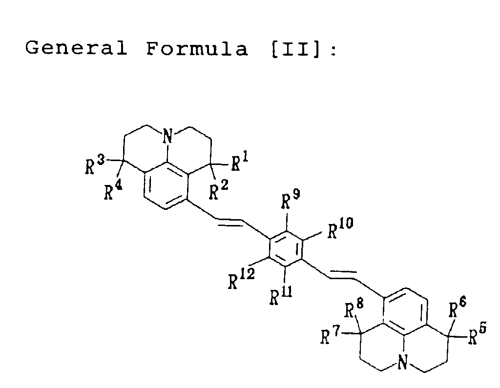
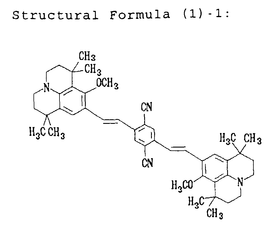
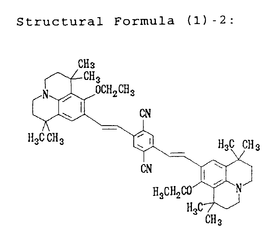
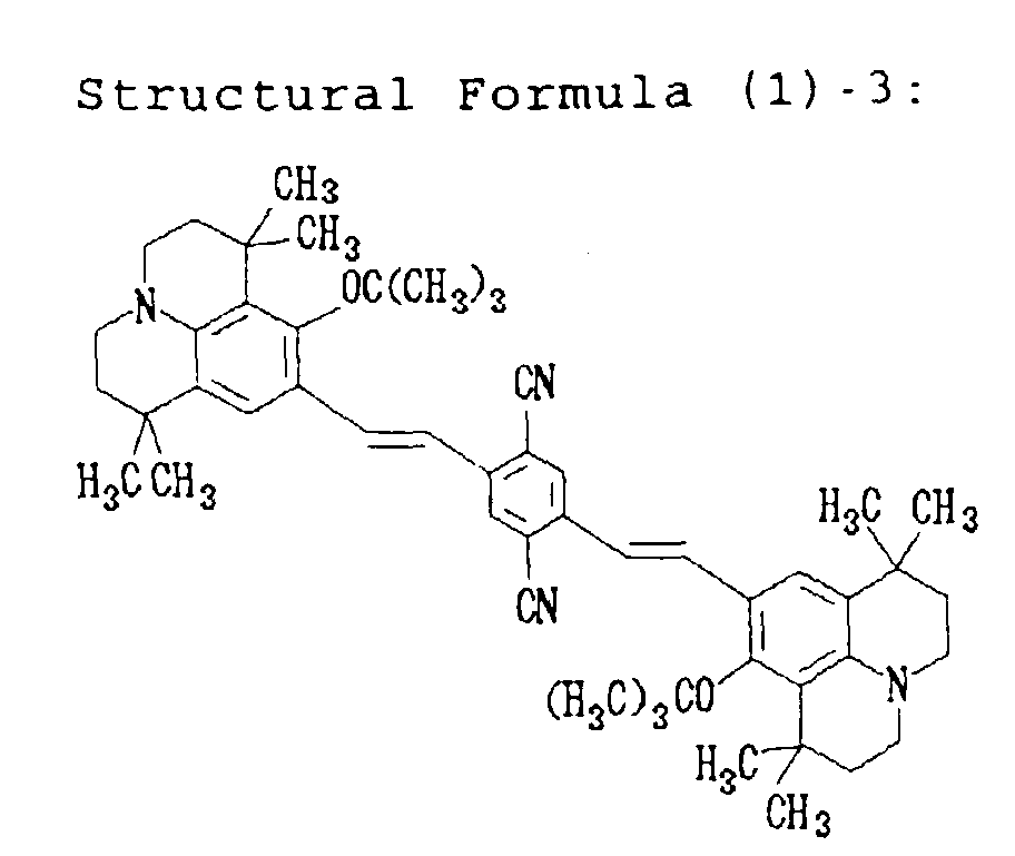


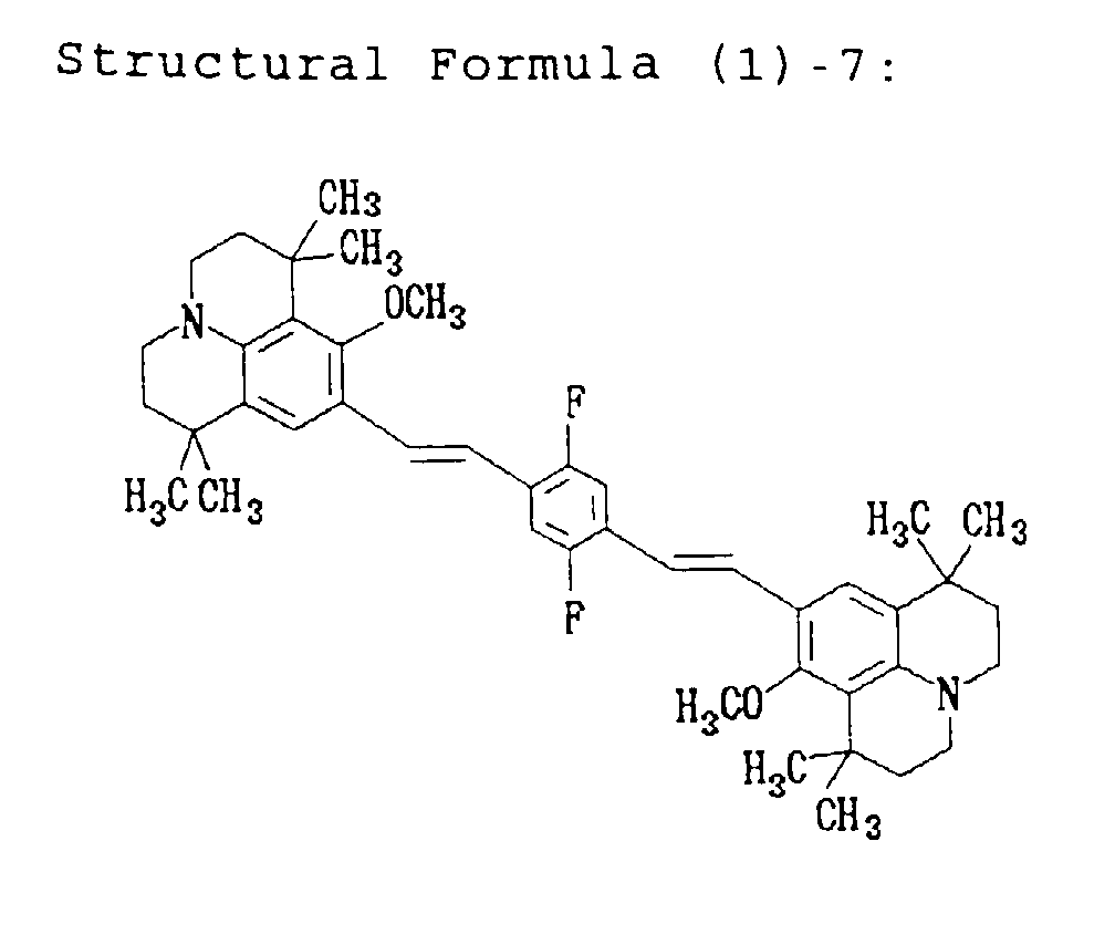
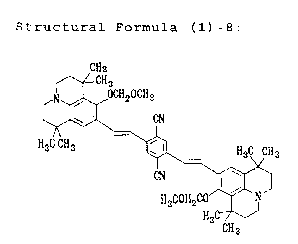
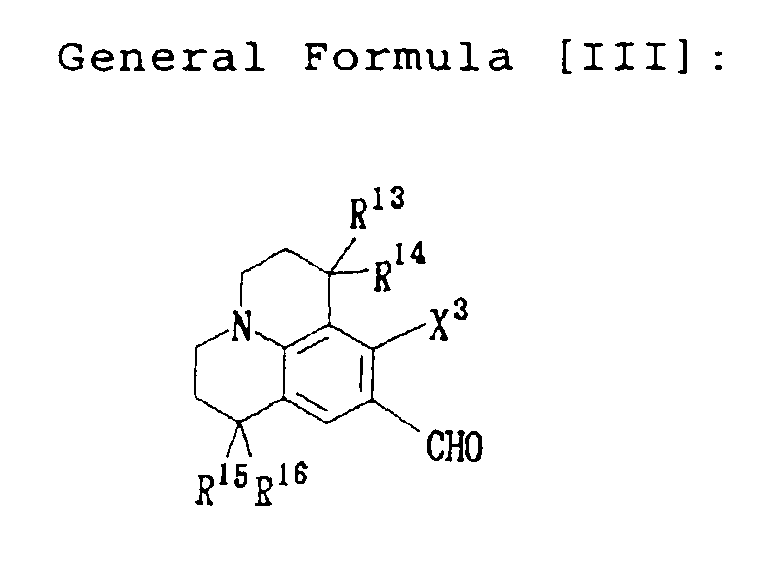 wherein X3 represents a hydrogen atom, a hydroxyl group, an alkoxyl group, an alkyl group, an amino group, an alkylamino group, or a substituted or unsubstituted aryl group corresponding to X1 and X2 defined before, respectively, R13, R14, R15 and R16, respectively, represent a lower alkyl group corresponding to R1, R2, R3, R4, R5, R6, R7 and R8 defined before and may be the same or different;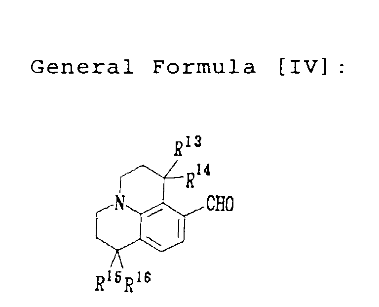
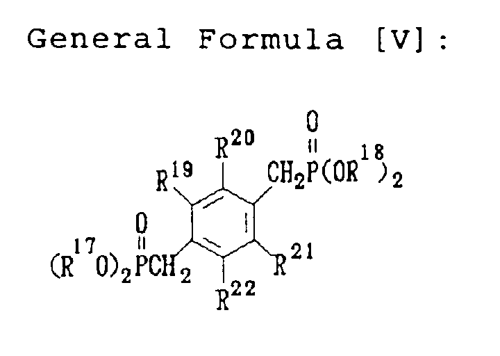 wherein R17 and R18 may be the same or different and independently represent a hydrocarbon group, R19, R20, R21 and R22, respectively, represent an electron attracting group corresponding to R9, R10, R11 and R12 defined before and may be the same or different, and Y represents a halogen atom such as a chlorine atom.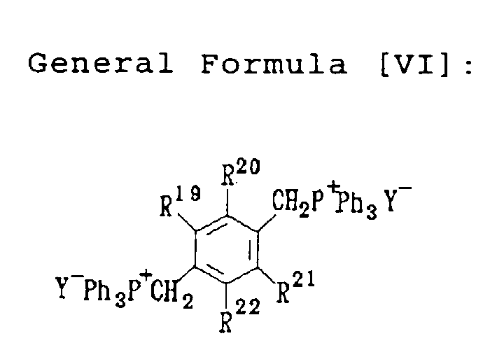


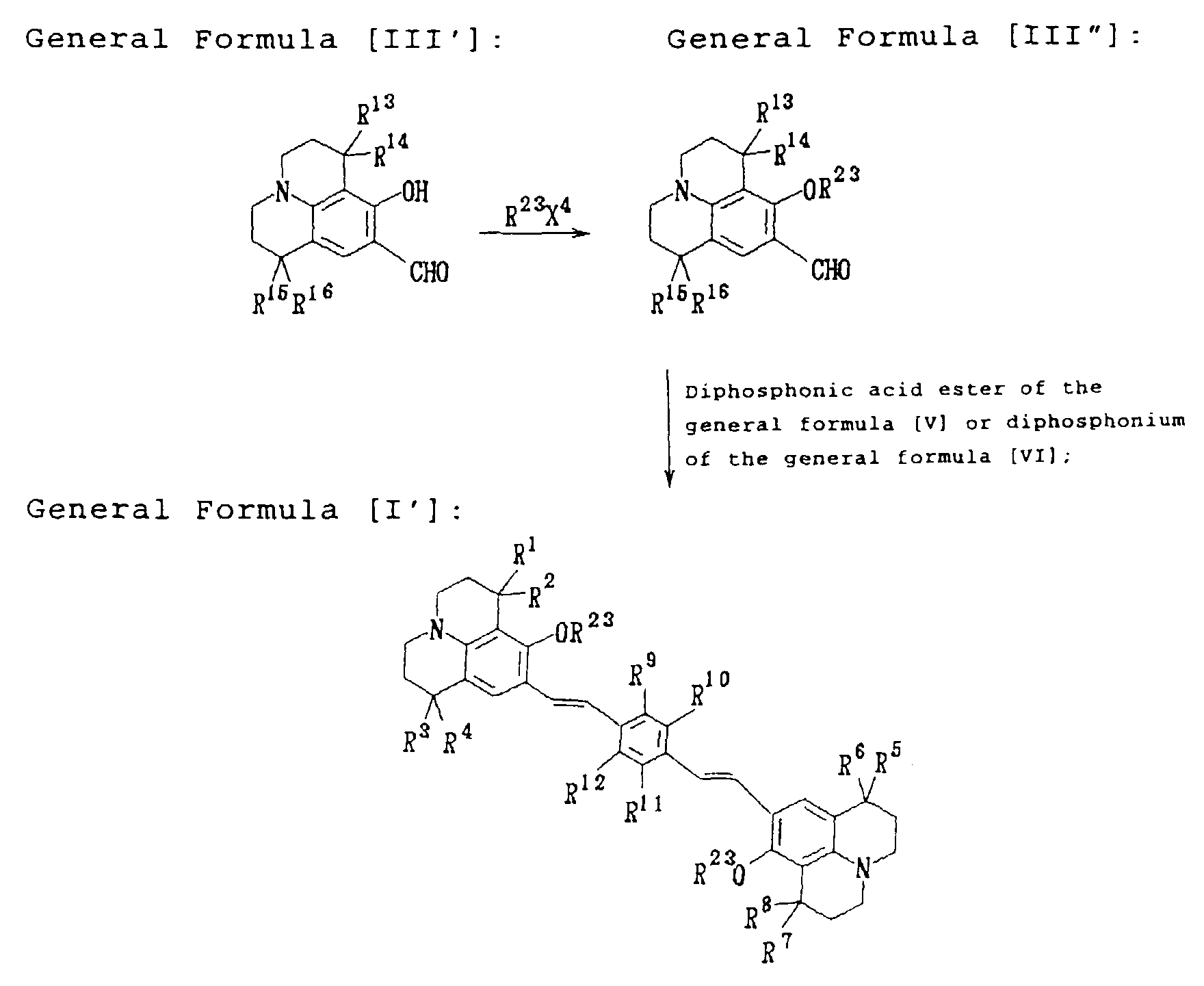 In the general formulae [I'], [I"], [III'] and [III"], R1, R2, R3, R4, R5, R6, R7, R8, R9, R10, R11, R12, R13, R14, R15 and R16, respectively, have the same meanings as defined before, R23 represents an alkyl group preferably having 1 to 6 carbon atoms such as a methyl group, an ethyl group or the like, or an alkoxyalkyl group preferably having 2 to 6 carbon atoms such as a methoxymethyl group or the like, and X4 represents a halogen atom such as, for example, a chlorine atom, an iodine atom or the like.
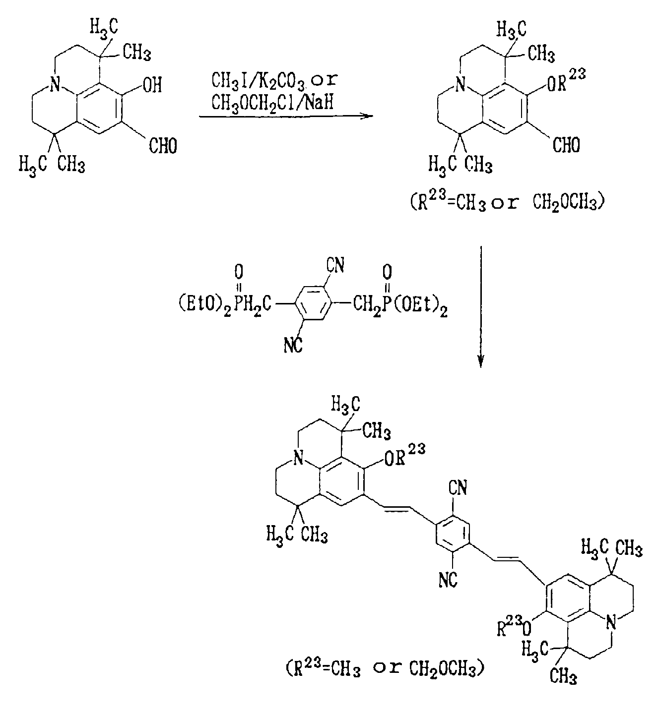

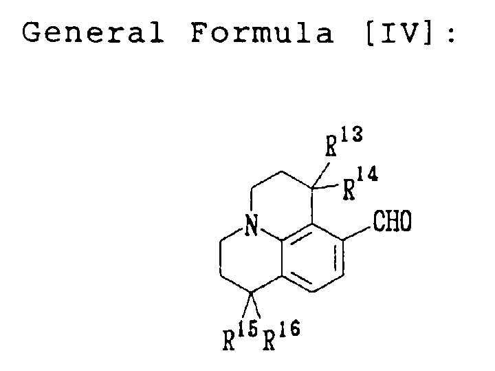


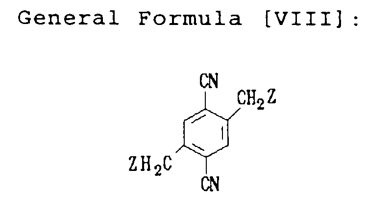


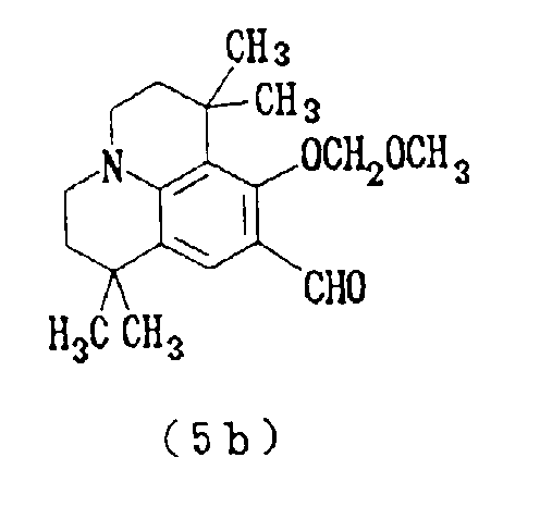


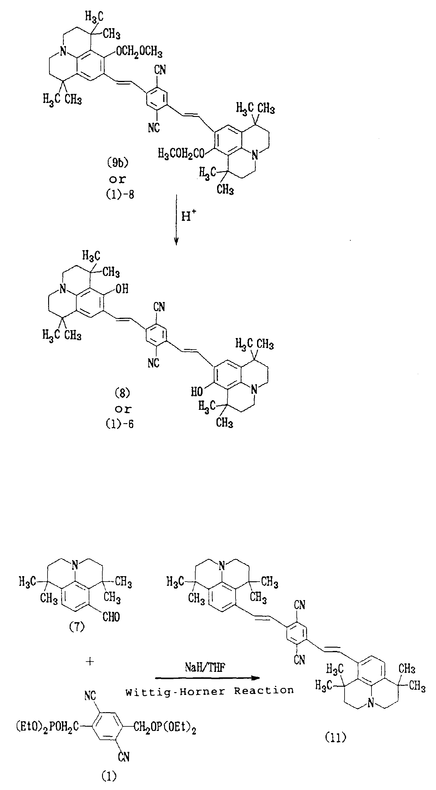
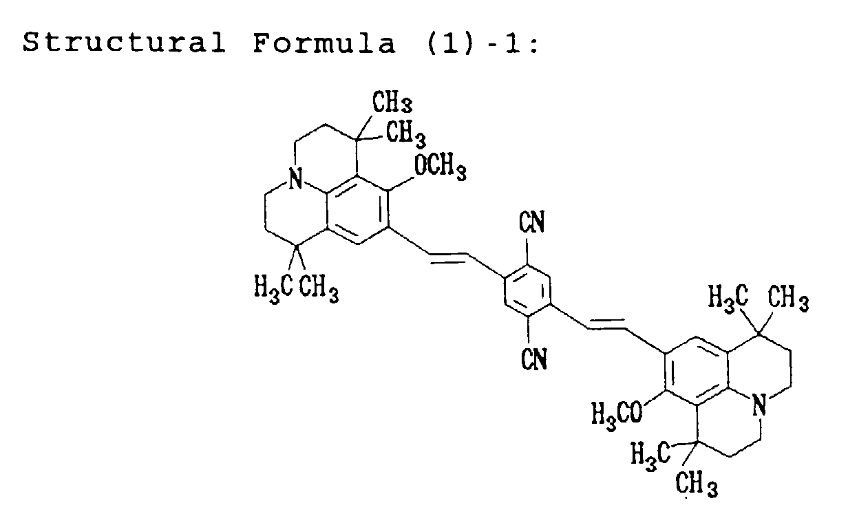


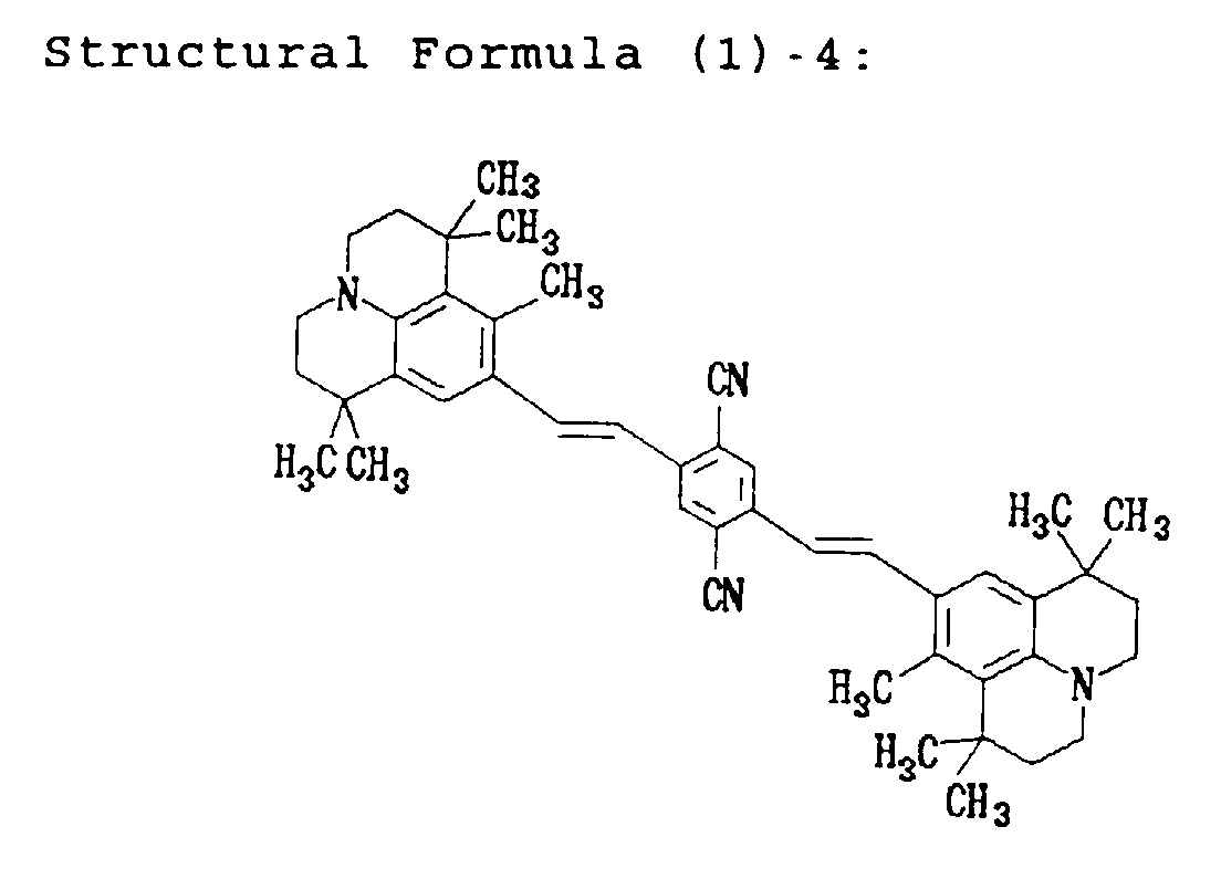
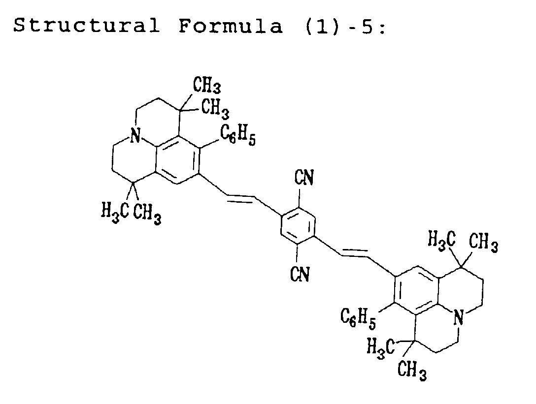
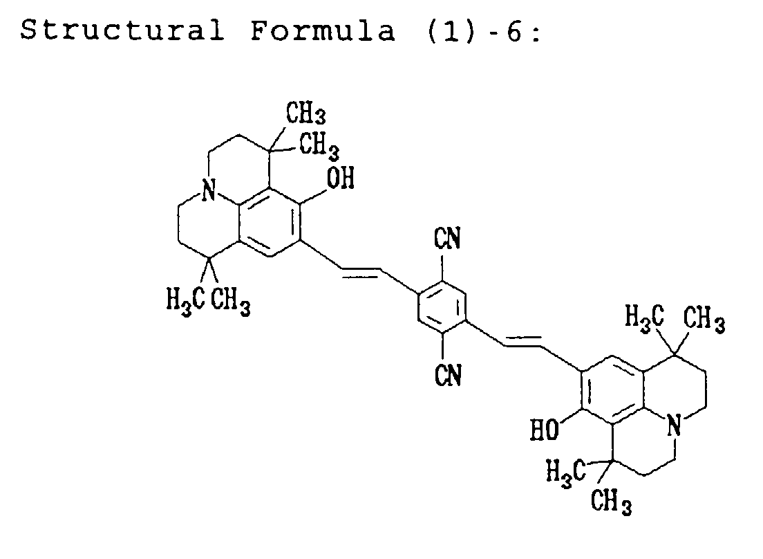
 wherein X1 and X2 may be the same or different and, respectively, represent a hydrogen atom, a hydroxyl group or a saturated or unsaturated, unsubstituted or substituted alkoxyl group, an alkyl group, an amino group, an alkylamino group, or a substituted or unsubstituted aryl group, R1, R2, R3, R4, R5, R6, R7 and R8 may be the same or different and independently represent a lower alkyl group, and R9, R10, R11 and R12 may be the same or different and at least one of them represents an electron attracting group.