EP1073117A2 - Scratch protection for direct contact sensors - Google Patents
Scratch protection for direct contact sensors Download PDFInfo
- Publication number
- EP1073117A2 EP1073117A2 EP00305713A EP00305713A EP1073117A2 EP 1073117 A2 EP1073117 A2 EP 1073117A2 EP 00305713 A EP00305713 A EP 00305713A EP 00305713 A EP00305713 A EP 00305713A EP 1073117 A2 EP1073117 A2 EP 1073117A2
- Authority
- EP
- European Patent Office
- Prior art keywords
- tungsten
- dielectric
- forming
- integrated circuit
- hardness
- Prior art date
- Legal status (The legal status is an assumption and is not a legal conclusion. Google has not performed a legal analysis and makes no representation as to the accuracy of the status listed.)
- Withdrawn
Links
Images


Classifications
-
- H—ELECTRICITY
- H10—SEMICONDUCTOR DEVICES; ELECTRIC SOLID-STATE DEVICES NOT OTHERWISE PROVIDED FOR
- H10W—GENERIC PACKAGES, INTERCONNECTIONS, CONNECTORS OR OTHER CONSTRUCTIONAL DETAILS OF DEVICES COVERED BY CLASS H10
- H10W44/00—Electrical arrangements for controlling or matching impedance
- H10W44/601—Capacitive arrangements
-
- G—PHYSICS
- G06—COMPUTING OR CALCULATING; COUNTING
- G06V—IMAGE OR VIDEO RECOGNITION OR UNDERSTANDING
- G06V40/00—Recognition of biometric, human-related or animal-related patterns in image or video data
- G06V40/10—Human or animal bodies, e.g. vehicle occupants or pedestrians; Body parts, e.g. hands
- G06V40/12—Fingerprints or palmprints
- G06V40/13—Sensors therefor
- G06V40/1329—Protecting the fingerprint sensor against damage caused by the finger
-
- H—ELECTRICITY
- H10—SEMICONDUCTOR DEVICES; ELECTRIC SOLID-STATE DEVICES NOT OTHERWISE PROVIDED FOR
- H10W—GENERIC PACKAGES, INTERCONNECTIONS, CONNECTORS OR OTHER CONSTRUCTIONAL DETAILS OF DEVICES COVERED BY CLASS H10
- H10W20/00—Interconnections in chips, wafers or substrates
- H10W20/40—Interconnections external to wafers or substrates, e.g. back-end-of-line [BEOL] metallisations or vias connecting to gate electrodes
- H10W20/45—Interconnections external to wafers or substrates, e.g. back-end-of-line [BEOL] metallisations or vias connecting to gate electrodes characterised by their insulating parts
- H10W20/48—Insulating materials thereof
Definitions
- the present invention relates generally to scratch protection for integrated sensor circuits, and more specifically to improvement of scratch protection in capacitive sensor circuits through selection of metallization materials.
- Fingerprint acquisition circuits employ arrays of sensors coated with a dielectric onto which the finger is placed with the epidermis in contact with the dielectric. The ridges and grooves on the epidermal layer of the finger are then detected by the sensors, which transmit signals representative of the detected pattern.
- various sensors e.g., resistive, etc.
- capacitive sensors have been found to provide the best performance. Since capacitance between two capacitive plates is inversely proportional to the distance between the plates, using the contacting dermal tissue itself as one capacitor plate and the sensor electrode as the other and then determining capacitance for each sensor electrode in the array, it is possible to locate the ridges and grooves of the fingerprint.
- Such capacitive sensors cannot be mechanically protected because physical contact on the surface of the integrated circuit with the finger is necessary.
- some scratch resistance protection for the capacitive sensor electrodes is required to prevent "scratch” damage to the sensor electrodes. Such damage typically results from undue (and unnecessary) pressure on the surface of the integrated circuit, alone or in combination with some sharp edge or protrusion such as a callous or scar, fingernail, dust or dirt particle, etc.
- SiC silicon carbide
- all metallization levels within the sensor circuit between the surface and the active regions of the substrate are formed of a conductive material having a hardness greater than that of aluminum.
- the selected conductive material preferably has a hardness which is at least as great as the lowest hardness for any interlevel dielectric or passivation material employed.
- the selected conductive material is employed for each metallization level between the surface and the active regions, including contacts and vias, landing pads, interconnects, capacitive electrodes, and electrostatic discharge protection lines.
- Tungsten is a suitable conductive material, for which existing processes may be substituted in place of aluminum metallization processes.
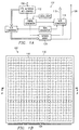
- Figure 1A depicts a block diagram of the sensor circuit 102 , which is formed as an integrated circuit on a single die.
- the sensor circuit 102 and its operation are described more fully in commonly assigned, copending application serial no. 09/040,261, entitled “CAPACITIVE DISTANCE SENSOR” and filed May 9, 1998, which is incorporated herein by reference.
- sensor circuit 102 relevant to the present invention include an array 104 of capacitive sensors for fingerprint acquisition by sensing distances between capacitive electrodes within the sensor array 104 and ridges and grooves on a finger placed in contact with sensor array 104 .
- Sensor circuit 102 also includes signal lines 106 and 108 and output bus 110 .
- Signal line 106 connects I 2 C interface and control device 104 , which provides a bidirectional communication protocol enabling sensor circuit 102 to communicate with a controller such as a microcontroller, with controller circuitry (not shown) external to sensor circuit 102 .
- Signal line 108 is a synchronization line coupling sensor array 104 to the external controller circuit, providing synchronization signals allowing detected voltages representative of the capacitive value of individual capacitive electrodes within sensor array 104 , and therefore representative of the distance between the capacitive electrode and the portion of the epidermal layer contacting sensor array 104 in the region of the capacitive electrode, to be properly interpreted by the external controller.
- Output bus 110 coupling an analog-to-digital (A/D) converter 114 to the external controller.
- A/D converter 114 processes analog voltage measurements received from sensor array 104 and generates digital representations recognized by the external controller as distance measurements of the analog measured voltages from individual capacitive electrodes within sensor array 104 .
- A/D converter 114 transmits these digital signals to the external controller on output bus 110 .
- Figure 1B is a pictorial representation of the "front" side of sensor circuit 102 ; that is, Figure 1B depicts the major surface of the die 116 on which the active devices constituting sensor circuit 102 are formed.
- Sensor array 104 is located on the front side of die 116 and includes a plurality of cells 118 , each containing one or more capacitive electrodes.
- Sensor array 104 in the exemplary embodiment contains square cells approximately 45-50 ⁇ m on a side, forming a 250 X 350 array of contiguous cells 118 within sensor array 104 .
- Sensor array 104 is covered by a passivation material overlying the capacitive electrodes within each cell 118 .
- Other active devices required to form sensor circuit 102 are formed below the capacitive electrodes.
- Figure 1C is a cross-sectional detail of a sensor array cell as seen from a cross-section taken along section line A-A .
- Sensor circuit 102 within a sensor array cell includes one or more active areas, such as polysilicon electrodes 120 or source/drain region 122 within a substrate 124 .
- a dielectric 126 overlies active areas 120 , 122 , with openings through which metal contacts 128 are formed to connect active regions 120 , 122 with metal regions 130 (e.g., landing pads or interconnects) within the first metallization level.
- An intermetal dielectric 132 overlies metal regions 130 and dielectric 126 , with openings therethrough in which are formed metal vias 134 connecting metal regions 130 to capacitive electrodes 136 overlying the interlevel dielectric 134 .
- Capacitive electrodes 136 are covered by a second intermetal dielectric 138 , on which are formed electrostatic discharge (ESD) protection patterns 140 .
- a passivation layer 142 which may actually comprise multiple layers, covers the ESD protection lines 142 and forms the surface 144 which is contacted by the epidermal layer of the finger during fmgerprint acquisition.
- a cause of "scratch" damage in capacitive sensor circuits of the type described above has been determined to be aluminum: the layer is too weak, and may delaminate, causing circuit failure, even if the passivation integrity is not violated.
- the hardness of various materials and material combinations is shown in the graph of Figure 2 . The hardness of materials for which the graph label includes an asterik ("*") were taken from literature references, while the other hardness values were determined experimentally.
- silicon dioxide (“quartz,” or simply “oxide”), which is commonly employed as an interlevel dielectric, has a hardness of slightly less than 10 gigaPascals (GPa).
- Silicon carbide (SiC), which is a suitable passivation material, and silicon together have an even greater hardness, comparable to that of diamond-like carbon (DLC).
- DLC diamond-like carbon
- aluminum the most common metallization material, has a hardness much lower than quartz.
- a capacitive sensor circuit of the type described above typically includes a plurality of layer, including: silicon carbide and silicon nitride, which form a suitable passivation layer; silicon dioxide, a suitable interlevel dielectric; aluminum, the most commonly-employed metal for metallization levels; and silicon, the conventional material for an integrated circuit substrate.
- silicon carbide and silicon nitride which form a suitable passivation layer
- silicon dioxide a suitable interlevel dielectric
- aluminum the most commonly-employed metal for metallization levels
- silicon the conventional material for an integrated circuit substrate.
- a sequence of layers of different materials is unlikely to have a total hardness significantly greater than that of the constituent material having the lowest hardness.
- micro scratch results within Figure 2 for the sequence of layers described above demonstrate that the combined hardness is, as expected, not significantly greater than that of aluminum alone.
- Tungsten (W) has a suitable hardness, as illustrated in Figure 2 by micro scratch results for the sequence of layers described above with tungsten substituted for aluminum (i.e., SiC/SiN/SiO 2 /W/Si).
- Other suitably hard conductive materials include copper (Cu) and titanium nitride (TiN), and perhaps conductive polysilicon.
- the hardness of the conductive material selected for the metallization levels should preferably exceeds the lowest hardness of any other material employed. In most structures, the material (other than aluminum) having the lowest hardness will commonly be the interlevel dielectric oxide. Any material having a hardness greater than that of aluminum, however, will provide better scratch resistance protection.
- Capacitive electrodes 302 are connected to underlying conductive polysilicon structures 304 , which may be gate electrodes, source/drain contacts, or interconnects, through an interlevel dielectric 306 and a lower dielectric layer 308 .
- the conductive regions 312 connecting capacitive electrodes 302 to polysilicon conductors 304 , together with the capacitive electrodes 302 themselves and ESD protection lines 314 within passivation 316 are all formed of a conductive material having a hardness greater than that of aluminum.
- Tungsten is preferable since the hardness of tungsten provides suitable scratch resistance and known processes for forming tungsten contacts, vias, and interconnects may be readily substituted for aluminum metallization processes.
- Other metals for which processing techniques are now known or may be developed, such as copper, may also be employed if sufficiently hard.
- aluminum conductive regions may be employed to connect ESD protection lines 314 to underlying circuitry and for pads 322 .
- tungsten may alternatively be employed for all metallization levels in all areas of the sensor circuit.
- the present invention improves the performance and lifetime of sensor circuits for which direct physical contact with a finger, stylus, or other object is required.
Landscapes
- Engineering & Computer Science (AREA)
- Human Computer Interaction (AREA)
- Physics & Mathematics (AREA)
- General Physics & Mathematics (AREA)
- Multimedia (AREA)
- Theoretical Computer Science (AREA)
- Semiconductor Integrated Circuits (AREA)
- Measurement Of Length, Angles, Or The Like Using Electric Or Magnetic Means (AREA)
- Internal Circuitry In Semiconductor Integrated Circuit Devices (AREA)
- Measuring Fluid Pressure (AREA)
- Parts Printed On Printed Circuit Boards (AREA)
Abstract
Description
Claims (23)
- An integrated circuit structure, comprising:a capacitive electrode;a dielectric underlying the capacitive electrode; andan active region underlying the dielectric,
wherein the capacitive electrode and each conductive region between the capacitive electrode and the active region are formed of a conductive material having a hardness greater than a hardness of aluminum. - The integrated circuit structure of claim 1, wherein the capacitive electrode and each conductive region between the capacitive electrode and the active region are formed of a conductive material having a hardness at least as great as a hardness of the dielectric.
- The integrated circuit structure of claim 1, further comprising:a passivation layer over the capacitive electrode,
wherein the capacitive electrode and each conductive region between the capacitive electrode and the active region are formed of a conductive material having a hardness at least as great as a hardness of the passivation layer. - The integrated circuit structure of claim 1, wherein the capacitive electrode and each conductive region between the capacitive electrode and the active region are formed of tunsten.
- The integrated circuit structure of claim 4, further comprising:a tungsten via beneath the capacitive electrode.
- The integrated circuit structure of claim 5, further comprising:a tungsten interconnect beneath the via.
- The integrated circuit structure of claim 6, further comprising: a tungsten contact between the interconnect and the active region.
- The integrated circuit structure of claim 7, wherein the active region is a gate electrode.
- An integrated circuit structure, comprising:an active region;a dielectric overlying the active region and having a contact opening therethrough;a tungsten contact within the contact opening;a tungsten metal region overlying the contact and a portion of the dielectric;an interlevel dielectric overlying the tungsten metal region and the dielectric and having an opening therethrough;a tungsten via within the opening through the interlevel dielectric; anda tungsten capacitive electrode overlying the tungsten via and a portion of the interlevel dielectric, wherein the capacitive electrode is electrically connected to the active region by the contact, the metal region, and the via.
- The integrated circuit structure of claim 9, further comprising:an oxide over the capacitive electrode and the interlevel dielectric adjacent the capacitive electrode;a passivation layer including a silicon nitride layer and a silicon carbide layer over the oxide; andtungsten ESD protection within the passivation layer.
- An integrated circuit, comprising:an array of capacitive electrodes in a central portion of the integrated circuit; andESD protection devices and contact pads around a periphery of the integrated circuit,
wherein the capacitive electrodes and every metallization region beneath the array of capacitive electrodes within the central portion of the integrated circuit is formed of a material having a hardness greater than aluminum while at least one metallization region beneath an ESP protection device or contact pad is formed of aluminum. - The integrated circuit of claim 11, wherein every metallization region within the central portion of the integrated circuit is formed of tungsten.
- The integrated circuit of claim 12, further comprising:tungsten ESD protection above and between capacitive electrodes within the array of capactive electrodes and within the central portion of the integrated circuit, wherein each capacitive electrode within the array is formed of tungsten;tungsten vias beneath each capacitive electrode;tungsten interconnects beneath each tungsten via;tungsten contacts beneath each tungsten interconnect; andactive regions beneath each tungsten contact.
- A method of forming a scratch resistant integrated circuit structure, comprising:forming an active region;forming a dielectric overlying the active region; andforming a capacitive electrode overlying the dielectric, wherein the capacitive electrode and each conductive region between the capacitive electrode and the active region are formed of a conductive material having a hardness greater than a hardness of aluminum.
- The method of claim 14, wherein the capacitive electrode and each conductive region between the capacitive electrode and the active region are formed of tunsten.
- The method of claim 15 ,further comprising:forming a tungsten via beneath the capacitive electrode.
- The method of claim 16,further comprising:forming a tungsten interconnect beneath the via.
- The method of claim 17, further comprising:forming a tungsten contact between the interconnect and the active region.
- A method of forming an integrated circuit structure, comprising:forming an active region;forming a dielectric overlying the active region and having a contact opening therethrough;forming a tungsten contact within the contact opening;forming a tungsten metal region overlying the contact and a portion of the dielectric;forming an interlevel dielectric overlying the tungsten metal region and the dielectric and having an opening therethrough;forming a tungsten via within the opening through the interlevel dielectric; andforming a tungsten capacitive electrode overlying the tungsten via and a portion of the interlevel dielectric, wherein the capacitive electrode is electrically connected to the active region by the contact, the metal region, and the via.
- A method of forming a scratch resistant integrated circuit structure, comprising:forming a plurality of active regions;forming a dielectric over the plurality active regions; andforming an array of capacitive electrodes overlying the dielectric of a conductive material having a hardness at least as great as a hardness of the dielectric.
- The method of claim 20 wherein the step of forming an array of capacitive electrodes overlying the dielectric of a conductive material having a hardness at least as great as a hardness of the dielectric further comprises:forming the array of capacitive electrodes of a conductive material having a hardness at least as great as a hardness of a passivation layer overlying the array of conductive electrodes.
- The method of claim 20 wherein the step of forming an array of capacitive electrodes overlying the dielectric of a conductive material having a hardness at least as great as a hardness of the dielectric further comprises:forming the array of capacitive electrodes of tungsten.
- The method of claim 20 further comprising:forming each metallization region between the array of capacitive electrodes and the plurality of active regions of a conductive material having a hardness at least as great as the hardness of the dielectric.
Applications Claiming Priority (2)
| Application Number | Priority Date | Filing Date | Title |
|---|---|---|---|
| US360839 | 1989-06-02 | ||
| US09/360,839 US6423995B1 (en) | 1999-07-26 | 1999-07-26 | Scratch protection for direct contact sensors |
Publications (2)
| Publication Number | Publication Date |
|---|---|
| EP1073117A2 true EP1073117A2 (en) | 2001-01-31 |
| EP1073117A3 EP1073117A3 (en) | 2005-07-06 |
Family
ID=23419607
Family Applications (1)
| Application Number | Title | Priority Date | Filing Date |
|---|---|---|---|
| EP00305713A Withdrawn EP1073117A3 (en) | 1999-07-26 | 2000-07-06 | Scratch protection for direct contact sensors |
Country Status (2)
| Country | Link |
|---|---|
| US (5) | US6423995B1 (en) |
| EP (1) | EP1073117A3 (en) |
Cited By (3)
| Publication number | Priority date | Publication date | Assignee | Title |
|---|---|---|---|---|
| EP1347407A3 (en) * | 2002-03-20 | 2006-10-18 | Fujitsu Limited | Capacitance detection type sensor and manufacturing method thereof |
| US7606400B2 (en) | 2003-01-22 | 2009-10-20 | Nokia Corporation | Arrangement for authentication of a person |
| US8148686B2 (en) | 2003-01-22 | 2012-04-03 | Nokia Corporation | Sensing arrangement |
Families Citing this family (12)
| Publication number | Priority date | Publication date | Assignee | Title |
|---|---|---|---|---|
| US6423995B1 (en) * | 1999-07-26 | 2002-07-23 | Stmicroelectronics, Inc. | Scratch protection for direct contact sensors |
| DE19935910A1 (en) * | 1999-07-30 | 2001-02-08 | Siemens Ag | Passivation layer structure |
| US6603192B2 (en) * | 1999-07-30 | 2003-08-05 | Stmicroelectronics, Inc. | Scratch resistance improvement by filling metal gaps |
| FR2851258B1 (en) * | 2003-02-17 | 2007-03-30 | Commissariat Energie Atomique | METHOD OF COATING A SURFACE, FABRICATION OF MICROELECTRONIC INTERCONNECTION USING THE SAME, AND INTEGRATED CIRCUITS |
| FR2875082B1 (en) * | 2004-09-03 | 2006-11-10 | Atmel Nantes Sa Sa | INTEGRATED CIRCUIT WITH SECURITY SIGNAL CODE, SECURITY METHOD, DEVICE AND SECURITY SIGNAL CODE USING CORRESPONDING DYNAMIC KEY |
| US7582969B2 (en) * | 2005-08-26 | 2009-09-01 | Innovative Micro Technology | Hermetic interconnect structure and method of manufacture |
| JP4764508B2 (en) * | 2007-04-05 | 2011-09-07 | 富士通セミコンダクター株式会社 | Surface shape sensor and manufacturing method thereof |
| CN101668381B (en) * | 2008-09-03 | 2012-07-25 | 深圳富泰宏精密工业有限公司 | Electronic device |
| NO20093601A1 (en) | 2009-12-29 | 2011-06-30 | Idex Asa | surface Sensor |
| US9728567B2 (en) * | 2013-12-02 | 2017-08-08 | United Microelectronics Corp. | Semiconductor sensor device |
| US9465973B1 (en) * | 2015-03-19 | 2016-10-11 | Sunasic Technologies, Inc. | Enhanced capacitive fingerprint sensing unit |
| US10133905B2 (en) * | 2015-12-04 | 2018-11-20 | Sunasic Technologies, Inc. | Capacitive fingerprint sensing unit and enhanced capacitive fingerprint reader |
Family Cites Families (34)
| Publication number | Priority date | Publication date | Assignee | Title |
|---|---|---|---|---|
| US3771147A (en) * | 1972-12-04 | 1973-11-06 | Bell Telephone Labor Inc | Igfet memory system |
| US4290052A (en) * | 1979-10-26 | 1981-09-15 | General Electric Company | Capacitive touch entry apparatus having high degree of personal safety |
| US4353056A (en) | 1980-06-05 | 1982-10-05 | Siemens Corporation | Capacitive fingerprint sensor |
| US5190824A (en) * | 1988-03-07 | 1993-03-02 | Semiconductor Energy Laboratory Co., Ltd. | Electrostatic-erasing abrasion-proof coating |
| US6224952B1 (en) * | 1988-03-07 | 2001-05-01 | Semiconductor Energy Laboratory Co., Ltd. | Electrostatic-erasing abrasion-proof coating and method for forming the same |
| GB2244164A (en) | 1990-05-18 | 1991-11-20 | Philips Electronic Associated | Fingerprint sensing |
| EP0574213B1 (en) * | 1992-06-08 | 1999-03-24 | Synaptics, Inc. | Object position detector |
| US5463388A (en) * | 1993-01-29 | 1995-10-31 | At&T Ipm Corp. | Computer mouse or keyboard input device utilizing capacitive sensors |
| US5648674A (en) * | 1995-06-07 | 1997-07-15 | Xerox Corporation | Array circuitry with conductive lines, contact leads, and storage capacitor electrode all formed in layer that includes highly conductive metal |
| US5847690A (en) * | 1995-10-24 | 1998-12-08 | Lucent Technologies Inc. | Integrated liquid crystal display and digitizer having a black matrix layer adapted for sensing screen touch location |
| US5907627A (en) * | 1995-11-06 | 1999-05-25 | Dew Engineering And Development Limited | Contact imaging device |
| JP4024335B2 (en) * | 1996-01-26 | 2007-12-19 | ハリス コーポレイション | Integrated circuit device having an opening exposing die of integrated circuit and manufacturing method thereof |
| GB2310218B (en) * | 1996-02-13 | 1999-12-22 | Marconi Gec Ltd | Coatings |
| US6114862A (en) * | 1996-02-14 | 2000-09-05 | Stmicroelectronics, Inc. | Capacitive distance sensor |
| JPH113984A (en) * | 1997-06-13 | 1999-01-06 | Hitachi Ltd | Semiconductor integrated circuit device |
| TW365065B (en) * | 1997-07-19 | 1999-07-21 | United Microelectronics Corp | Embedded memory structure and manufacturing method thereof |
| US6240199B1 (en) * | 1997-07-24 | 2001-05-29 | Agere Systems Guardian Corp. | Electronic apparatus having improved scratch and mechanical resistance |
| US6483931B2 (en) * | 1997-09-11 | 2002-11-19 | Stmicroelectronics, Inc. | Electrostatic discharge protection of a capacitve type fingerprint sensing array |
| US6111247A (en) * | 1997-12-08 | 2000-08-29 | Intel Corporation | Passivation protection of sensor devices having a color filter on non-sensor portion |
| US6232142B1 (en) * | 1997-12-09 | 2001-05-15 | Seiko Epson Corporation | Semiconductor device and method for making the same, electro-optical device using the same and method for making the electro-optical device, and electronic apparatus using the electro-optical device |
| US6163313A (en) * | 1997-12-12 | 2000-12-19 | Aroyan; James L. | Touch sensitive screen and method |
| US6091132A (en) * | 1997-12-19 | 2000-07-18 | Stmicroelectronics, Inc. | Passivation for integrated circuit sensors |
| US5955781A (en) * | 1998-01-13 | 1999-09-21 | International Business Machines Corporation | Embedded thermal conductors for semiconductor chips |
| US6091082A (en) * | 1998-02-17 | 2000-07-18 | Stmicroelectronics, Inc. | Electrostatic discharge protection for integrated circuit sensor passivation |
| US6478976B1 (en) * | 1998-12-30 | 2002-11-12 | Stmicroelectronics, Inc. | Apparatus and method for contacting a conductive layer |
| US6346739B1 (en) * | 1998-12-30 | 2002-02-12 | Stmicroelectronics, Inc. | Static charge dissipation pads for sensors |
| US6686546B2 (en) * | 1998-12-30 | 2004-02-03 | Stmicroelectronics, Inc. | Static charge dissipation for an active circuit surface |
| US6330145B1 (en) * | 1998-12-30 | 2001-12-11 | Stmicroelectronics, Inc. | Apparatus and method for contacting a sensor conductive layer |
| US6326227B1 (en) * | 1998-12-30 | 2001-12-04 | Stmicroelectronics, Inc. | Topographical electrostatic protection grid for sensors |
| US6440814B1 (en) * | 1998-12-30 | 2002-08-27 | Stmicroelectronics, Inc. | Electrostatic discharge protection for sensors |
| US6204524B1 (en) * | 1999-07-14 | 2001-03-20 | Micron Technology, Inc. | CMOS imager with storage capacitor |
| US6423995B1 (en) * | 1999-07-26 | 2002-07-23 | Stmicroelectronics, Inc. | Scratch protection for direct contact sensors |
| US6603192B2 (en) * | 1999-07-30 | 2003-08-05 | Stmicroelectronics, Inc. | Scratch resistance improvement by filling metal gaps |
| US6515488B1 (en) * | 2001-05-07 | 2003-02-04 | Stmicroelectronics, Inc. | Fingerprint detector with scratch resistant surface and embedded ESD protection grid |
-
1999
- 1999-07-26 US US09/360,839 patent/US6423995B1/en not_active Expired - Lifetime
-
2000
- 2000-07-06 EP EP00305713A patent/EP1073117A3/en not_active Withdrawn
-
2001
- 2001-10-03 US US09/970,258 patent/US6780726B2/en not_active Expired - Lifetime
-
2002
- 2002-01-29 US US10/059,982 patent/US7687839B2/en not_active Expired - Lifetime
-
2010
- 2010-01-08 US US12/655,830 patent/US8039343B2/en not_active Expired - Fee Related
-
2011
- 2011-09-14 US US13/232,171 patent/US8633525B2/en not_active Expired - Fee Related
Cited By (5)
| Publication number | Priority date | Publication date | Assignee | Title |
|---|---|---|---|---|
| EP1347407A3 (en) * | 2002-03-20 | 2006-10-18 | Fujitsu Limited | Capacitance detection type sensor and manufacturing method thereof |
| US7364931B2 (en) | 2002-03-20 | 2008-04-29 | Fujitsu Limited | Capacitance detection type sensor and manufacturing method thereof |
| EP1944722A3 (en) * | 2002-03-20 | 2008-12-31 | Fujitsu Limited | Capacitance detection type sensor and manufacturing method thereof |
| US7606400B2 (en) | 2003-01-22 | 2009-10-20 | Nokia Corporation | Arrangement for authentication of a person |
| US8148686B2 (en) | 2003-01-22 | 2012-04-03 | Nokia Corporation | Sensing arrangement |
Also Published As
| Publication number | Publication date |
|---|---|
| US20120091517A1 (en) | 2012-04-19 |
| US8633525B2 (en) | 2014-01-21 |
| US6423995B1 (en) | 2002-07-23 |
| US6780726B2 (en) | 2004-08-24 |
| US7687839B2 (en) | 2010-03-30 |
| US8039343B2 (en) | 2011-10-18 |
| EP1073117A3 (en) | 2005-07-06 |
| US20020113259A1 (en) | 2002-08-22 |
| US20100117129A1 (en) | 2010-05-13 |
| US20020014651A1 (en) | 2002-02-07 |
Similar Documents
| Publication | Publication Date | Title |
|---|---|---|
| US8039343B2 (en) | Scratch protection for direct contact sensors | |
| US20030107097A1 (en) | Ultra-rugged biometric I.C. sensor and method of making the same | |
| US6740945B2 (en) | Apparatus and method for contacting a conductive layer | |
| EP1256899B1 (en) | Fingerprint detector with scratch resistant surface and embedded ESD protection grid | |
| US6326689B1 (en) | Backside contact for touchchip | |
| US6686546B2 (en) | Static charge dissipation for an active circuit surface | |
| US6829950B2 (en) | Method and apparatus for pressure sensing | |
| JP4308508B2 (en) | Capacitive fingerprint sensor with protective coating including conductive suspending agent | |
| US7071708B2 (en) | Chip-type sensor against ESD and stress damages and contamination interference | |
| US6330145B1 (en) | Apparatus and method for contacting a sensor conductive layer | |
| US6501142B2 (en) | Topographical electrostatic protection grid for sensors | |
| EP1073103A1 (en) | Backside bus vias | |
| JP2000196026A (en) | Electrostatic discharge protection for sensors | |
| US6603192B2 (en) | Scratch resistance improvement by filling metal gaps | |
| JP2004136090A (en) | Fingerprint detector with improved sensing surface layer | |
| JP2000194825A (en) | Fingerprint sensor device |
Legal Events
| Date | Code | Title | Description |
|---|---|---|---|
| PUAI | Public reference made under article 153(3) epc to a published international application that has entered the european phase |
Free format text: ORIGINAL CODE: 0009012 |
|
| AK | Designated contracting states |
Kind code of ref document: A2 Designated state(s): AT BE CH CY DE DK ES FI FR GB GR IE IT LI LU MC NL PT SE |
|
| AX | Request for extension of the european patent |
Free format text: AL;LT;LV;MK;RO;SI |
|
| PUAL | Search report despatched |
Free format text: ORIGINAL CODE: 0009013 |
|
| AK | Designated contracting states |
Kind code of ref document: A3 Designated state(s): AT BE CH CY DE DK ES FI FR GB GR IE IT LI LU MC NL PT SE |
|
| AX | Request for extension of the european patent |
Extension state: AL LT LV MK RO SI |
|
| 17P | Request for examination filed |
Effective date: 20051223 |
|
| AKX | Designation fees paid |
Designated state(s): DE FR GB IT |
|
| STAA | Information on the status of an ep patent application or granted ep patent |
Free format text: STATUS: THE APPLICATION IS DEEMED TO BE WITHDRAWN |
|
| 18D | Application deemed to be withdrawn |
Effective date: 20071124 |