EP1072662B1 - Chemical-mechanical abrasive composition and method - Google Patents
Chemical-mechanical abrasive composition and method Download PDFInfo
- Publication number
- EP1072662B1 EP1072662B1 EP00306436A EP00306436A EP1072662B1 EP 1072662 B1 EP1072662 B1 EP 1072662B1 EP 00306436 A EP00306436 A EP 00306436A EP 00306436 A EP00306436 A EP 00306436A EP 1072662 B1 EP1072662 B1 EP 1072662B1
- Authority
- EP
- European Patent Office
- Prior art keywords
- acid
- abrasive
- composition according
- chemical
- abrasion
- Prior art date
- Legal status (The legal status is an assumption and is not a legal conclusion. Google has not performed a legal analysis and makes no representation as to the accuracy of the status listed.)
- Expired - Lifetime
Links
Images

Classifications
-
- C—CHEMISTRY; METALLURGY
- C09—DYES; PAINTS; POLISHES; NATURAL RESINS; ADHESIVES; COMPOSITIONS NOT OTHERWISE PROVIDED FOR; APPLICATIONS OF MATERIALS NOT OTHERWISE PROVIDED FOR
- C09K—MATERIALS FOR MISCELLANEOUS APPLICATIONS, NOT PROVIDED FOR ELSEWHERE
- C09K3/00—Materials not provided for elsewhere
- C09K3/14—Anti-slip materials; Abrasives
- C09K3/1454—Abrasive powders, suspensions and pastes for polishing
- C09K3/1463—Aqueous liquid suspensions
-
- C—CHEMISTRY; METALLURGY
- C09—DYES; PAINTS; POLISHES; NATURAL RESINS; ADHESIVES; COMPOSITIONS NOT OTHERWISE PROVIDED FOR; APPLICATIONS OF MATERIALS NOT OTHERWISE PROVIDED FOR
- C09G—POLISHING COMPOSITIONS; SKI WAXES
- C09G1/00—Polishing compositions
- C09G1/02—Polishing compositions containing abrasives or grinding agents
-
- H—ELECTRICITY
- H10—SEMICONDUCTOR DEVICES; ELECTRIC SOLID-STATE DEVICES NOT OTHERWISE PROVIDED FOR
- H10P—GENERIC PROCESSES OR APPARATUS FOR THE MANUFACTURE OR TREATMENT OF DEVICES COVERED BY CLASS H10
- H10P52/00—Grinding, lapping or polishing of wafers, substrates or parts of devices
- H10P52/40—Chemomechanical polishing [CMP]
- H10P52/403—Chemomechanical polishing [CMP] of conductive or resistive materials
Definitions
- Chemical-mechanical polishing is a planarization technique which was developed to address the problem associated with the difficulty in focusing during a photolithography process for producing integrated circuits due to the difference in the thickness of deposited films.
- the chemical-mechanical polishing technique was first applied to the production of the elements with a size in the order of 0.5 microns. With the reduction in the size of elements, the chemical-mechanical polishing technique was applicable to an increased number of layers. Until the elements were developed to be in the order of 0.25 microns, the chemical-mechanical polishing became an important and essential planarization technique.
- the polishing method for producing a wire circuit comprises mounting a semiconductor wafer on a spinning platen equipped with an abrasive head and applying an abrasive slurry comprising abrasive particles and chemical additives to the surface of the wafer to enhance the abrasion performance.
- the CMP technique is the one which first modifies the surface to be polished by changing the chemical properties of the surface and then removes the modified surface in a mechanically abrasive manner.
- U. S. Patent No. 5,759,917 discloses a chemical-mechanical polishing composition and method for polishing silicon dioxide and silicon nitride in the production of semiconductors and integrated circuits.
- the composition of U. S. Patent No. 5,759,917 has a high selectivity for polishing silicon dioxide relative to silicon nitride and comprises a salt, a soluble cerium, and a carboxylic acid, and has a pH ranging from 3 to 11.
- U.S. Patent No. 5,861,054 discloses a polishing composition for use in polishing silicon dioxide and silicon nitride with a high selectivity for silicon dioxide relative to silicon nitride, which composition comprises an acidic solvent and silicon nitride with a primary particle size in the range of from 0.01 to 1000 nm.
- U.S. Patent No. 5,891,205 discloses a chemical-mechanical polishing composition for polishing semiconductor devices, which composition comprises an alkaline aqueous dispersion that contains mixed particles of cerium oxide and silicon dioxide.
- U.S. Pat. No. 5,084,071 discloses a method for polishing an electronic component substrate using of a chemical-mechanical polishing slurry, which polishing slurry comprises no more than weight percent of alumina, abrasive particles (e.g.
- U.S. Pat. No. 5,336,542 discloses a polishing composition comprising alumina abrasive particles and a chelating agent selected from the group consisting of polyaminocarboxylic acid (e.g. EDTA) and the sodium and potassium salts thereof.
- the composition of U.S. Pat. No. 5,336,542 may further comprise boehmite or an aluminum salt.
- One object of the present invention is to provide a chemical-mechanical abrasive composition which can effectively enhance the removal rate of a dielectric layer in either an acidic or a basic medium.
- the materials which can be used as dielectrics include silicon dioxide, silicon nitride, borophosphosilicate glass (BPSG), and those having a low dielectric constant (low-k), and the composites thereof. It has been discovered that the chemical-mechanical abrasive composition of the present invention is also effective in polishing polysilicon.
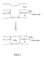
- a chemical-mechanical polishing slurry should be used to planarize the silicon dioxide layer and stop at the silicon nitride layer.
- the removal rate of silicon dioxide to silicon nitride should be at least greater than 3.
- another object of the present invention is to provide a chemical-mechanical abrasive composition for use in the polishing of semiconductor devices, which composition is able to provide a ratio of greater than 3 of the removal rate of silicon dioxide to that of silicon nitride.
- the polishing method should involve several steps.
- an abrasive slurry is used to polish the copper film of a semiconductor and stops at the tantalum nitride (TaN) layer, wherein the ratio of the removal rate of the copper film to that of the tantalum nitride layer should be at least greater than 3.
- the second step as shown in Figure 2(b) , another abrasive slurry is used to polish the tantalum nitride layer and the copper film of the semiconductor and stops at a dielectric layer, wherein the ratio of the removal rate of the tantalum nitride layer to that of the copper film should be at least greater than 1. Since in the first and second steps, the copper film may be subjected to a dishing phenomenon, a third step of over-polishing, as shown in Figure 2(c) , may be needed. The third abrasive slurry used in the third step should achieve a removal rate of the dielectric layer that is greater than or the same as that of the copper film and tantalum nitride layer.
- U.S. Pat. No. 5,114,437 discloses a polishing composition for an aluminum substrate, said composition comprising an alumina polishing agent having an average particle size of 0.2 to 5 ⁇ m, and a polishing accelerator selected from the group consisting of chromium(III) nitrate, lanthanum nitrate, ammonium cerium (III) nitrate, and neodymium nitrate.
- U.S. Pat. No. 5,209,816 discloses a method for polishing an Al- or Ti-containing metal layer with a chemical-mechanical abrasive slurry.
- the abrasive slurry contains, in addition to a solid abrasive material, about 0.1-20% by volume H 3 PO 4 and about 1-30% by volume of H 2 O 2 .
- U.S. Pat. No. 5,225,034 discloses a chemical-mechanical abrasive slurry, which comprises AgNO 3 , solid abrasive particles, and an oxidant selected from H 2 O 2 , HOCl, KOCl, KMgO 4 , or CH 3 COOOH.
- the slurry is used for polishing the copper layer on a semiconductor wafer so as to produce copper wires on the wafer.
- 5,340,370 discloses a chemical-mechanical polishing slurry for tungsten or tungsten nitride film, which comprises an oxidizing agent such as potassium ferricyanide, an abrasive, and water, and has a pH range between 2 and 4.
- U.S. Pat. No. 5,516,346 discloses a slurry for chemical mechanically polishing a titanium film, said slurry comprising potassium fluoride in a concentration sufficient to complex with said titanium film, and an abrasive such as silica, and having a pH level less than 8.
- Yet another object of the present invention is to provide a chemical-mechanical abrasive composition which can effectively improve the removal rate of metals.
- the chemical-mechanical composition of the invention can provide the same or different abrasion selectivities to the metal wires and dielectric layers in integrated circuits.
- EP-A-984049 published on 8 March 2000 (Eternel Chemical Coltd), describes an abrasive composition which comprises 70-95% by weight of an aqueous medium, 1-25% by weight of an abrasive and 0.1-20% by weight of an abrasion accelerator, where the abrasion accelerator comprises a monocarboxy group- or an amido group-containing compound and optionally a nitrate salt.
- the invention provides a chemical-mechanical abrasive composition for use in semiconductor processing, which comprises an aqueous medium, an abrasive, and an abrasion accelerator as set out in claim 1.
- the abrasion accelerator mainly functions to enhance the removal rate of the substances to be removed, and can be selected from the compounds of the following formula, the acid-addition salts thereof, or mixtures of two or more of the foregoing compounds and salts: wherein X and Y are independently O, S or NH; R 1 and R 2 are independently H, amino, aminoalkyl, or alkoxyo:
- Preferably the following compounds are excluded: formic acid, acetic acid, propionic acid, butyric acid, valeric acid, hexanoic acid, glycolic acid, lactic acid and the salts thereof; glycine, sarcosine, dimethylglycine, alanine and the salts thereof; and foramide, acetamide, propionamide, N-methylforamide, N-
- the invention further provides an method of using the above chemical-mechanical abrasive composition for polishing the surface of a semiconductor wafer, as set out in claim 12.
- the invention relates to a chemical-mechanical abrasive composition for effectively polishing the surface of a semiconductor wafer, said composition comprising an aqueous medium, an abrasive, and an abrasion accelerator.
- the abrasive composition of the invention may comprise from 0.1 to 30% by weight, and preferably from 3 to 25% by weight of the abrasive, and from 0.01 to 5 % by weight, and preferably 0.03 to 2% by weight of the abrasion accelerator.
- the entire planarization of a wafer surface is accomplished by chemical-mechanical abrasion.
- the substances removed from the wafer surface may re-bond to the wafer surface and be deposited on the wafer surface. This will not only reduce the abrasion rate and the planarization extent, but also cause defects to form on the wafer surface. Consequently, there is a need for compounds with a chelation ability to facilitate the removal of the substances to be removed from the wafer surface, so as to avoid the re-bonding of these substances to the wafer surface.
- the present invention provides an abrasion accelerator with a better chelation property.
- the abrasion accelerator of the invention can be selected from the compounds of the following formula, the acid-addition salts thereof, and mixtures of two or more of the foregoing compounds and salts: wherein X and Y independently O, S or NH; R 1 and R 2 are independently H, C 1 -C 6 alkyl, amino, aminoC 1 -C 6 alkoxy with the proviso that the following compounds are excluded: formic acid, acetic acid, propionic acid, butyric acid, valeric acid, hexanoic acid, glycolic acid, lactic acid and the salts thereof; glycine, sarcosine, dimethylglycine, alanine and the salts thereof; and foramide, acetamide, propionamide, N-methylforamide, N-methylacetamide, urea, methylurea, ethylurea, dimethylurea and diethylurea.
- the mechanism involved by the abrasion accelerator compounds of the invention to chelate the atoms or atomic groups of substances, thereby removing said substances, is believed to be as follows: wherein M is an atom or atomic group of the substances to be removed, and n is the valence charge of M.
- the abrasive composition of the invention can enhance the abrasion rate no matter whether the abrasion is conducted in an acidic, neutral, or basic condition.
- the abrasive used in the abrasive composition of the invention can be any commercially available abrasive, such as SiO 2 , Al 2 O 31 , ZrO 2 , CeO 2 , SiC, Fe 2 O 3 , TiO 2 , Si 3 N 4 , or a mixture thereof. These abrasives normally have the advantages of high purity, high surface area, and narrow particle size distribution, and are thus suitable for use in abrasive compositions as abrasive particles.
- the chemical-mechanical abrasive composition of the invention can be formulated to have a desired constitution by altering the species and concentration of the abrasion accelerator or the amount of the abrasive particles.
- the abrasion accelerators in the invention include methyl glycinate, glycinamide, aminoguanidine, semicarbazide, guanidine, formamidine, acetamidine, formyl hydrazide, acethydrazide, ethyl glycinate, methyl carbazate, ethyl carbazate, methyl carbamate, or ethyl carbamate, or an acid-addition salt thereof, such as the hydrochloride, nitrate, carbonate, or sulfate salt thereof, or a derivative with a similar structure thereof, or a mixture of two or more of the foregoing compounds.
- the abrasion accelerator is selected from the group consisting of methyl glycinate hydrochloride, glycinamide hydrochloride, aminoguanidine carbonate, semicarbazide hydrochloride, guanidine carbonate, and a mixture thereof.
- the chemical-mechanical abrasive composition of the invention may optionally comprise from 0.001 to 2% by weight of an acidic component and/or the salt thereof to further enhance the abrasion rate.
- the acidic component which may be used in the present invention, could be any commercially available acid, such as nitric acid, hydrogen chloride, sulfuric acid, sulfurous acid, phosphoric acid, phosphorous acid, chloric acid, bromic acid, iodic acid, perchloric acid, perbromic acid, periodic acid, malonic acid, succinic acid, glutaric acid, dipic acid, glycolic acid, lactic acid, citric acid, malic acid, tartaric acid, oxalic acid, glycine or creatine, or a mixture thereof.
- the composition of the invention may comprise ammonium carbonate to further enhance the abrasion rate
- the chemical-mechanical abrasive composition of the present invention may use water as a medium.
- water and preferably conventional deionized water, may be used to make the abrasive composition to be in the form of a slurry.
- the chemical mechanical abrasive composition of the present invention may further comprise other ingredients which are conventionally used in chemical mechanical abrasive compositions, only if they do not cause any adverse effect on the abrasive composition of the present invention. Therefore, the chemical-mechanical abrasive composition of the present invention may optionally comprise 0.1 to 10%, preferably 0.1 to 5% and more preferably 1 to 3% by weight of an oxidant conventionally used in the art, such as H 2 O 2 , Fe(NO 3 ) 3 , KIO 3 , CH 3 COOOH, or KMnO 4 .
- an oxidant conventionally used in the art, such as H 2 O 2 , Fe(NO 3 ) 3 , KIO 3 , CH 3 COOOH, or KMnO 4 .
- Species of wafer for abrasion test Species of film Formation of film Deposition thickness ( ⁇ ) TEOS Chemical vapor deposition 8000 SiO 2 Thermal oxidation 8000 Si 3 N 4 Chemical vapor deposition 3000 W Chemical vapor deposition 8000 TaN Chemical vapor deposition 5000 Cu Chemical vapor deposition 8000 TiN Chemical vapor deposition 5000 B.
- Abrasion platen IPEC/Westech 472 C. Temperature: 25°C D.
- Pad type IC 1400 manufactured by Rodel Company E. Flow rate of slurry: 150 ml/min
- the thickness of a dielectric layer can be directly determined by an optical method.
- the present invention used Model SM 300, manufactured by KLA-Tencor Company, to determine the thickness of a dielectric layer.
- the thickness of a metal layer is determined by using Model RS 75, manufactured by KLA-Tencor Company.
- the thickness of a film should be measured by a thickness measuring means.
- the sheet resistivity of a metal film is measured by a 4-point probe.
- the abrasion rate is determined as follows:
- Chemical-mechanical abrasive slurries respectively containing methyl glycinate hydrochloride, glycinamide hydrochloride, and aminoguanidine carbonate were prepared.
- the resultant slurries were used to polish TEOS film under the following conditions:
- Chemical-mechanical abrasive slurries respectively containing semicarbazide hydrochloride, aminoguanidine carbonate, and guanidine carbonate were prepared.
- the resultant slurries were used to polish SiO 2 film under the following conditions:
- Chemical-mechanical abrasive slurries respectively containing aminoguanidine carbonate, semicarbazide hydrochloride, and guanidine carbonate were prepared.
- the resultant slurries were used to polish TEOS and silicon nitride films under the following conditions:
- Chemical-mechanical abrasive slurries respectively containing semicarbazide hydrochloride, aminoguanidine carbonate, and guanidine carbonate, and having a pH value ranging from 3.8 to 4.6 were prepared.
- the resultant slurries were used to polish copper, tantalum nitride, and TEOS films under the following conditions:
- the abrasive compositions illustrated in Example 4 can be used in semiconductor abrasion processing to produce a pattern as shown in Figure 2 .
- the abrasive compositions of Run 1 and Run 2 can be used in the first step; the abrasive composition of Run 3 can be used in the second step; and the abrasive compositions of Run 4 to Run 6 can be used in the third step.
- Chemical-mechanical abrasive slurries respectively containing semicarbazide hydrochloride, aminoguanidine carbonate, and guanidine carbonate, and having a pH value ranging from 3.8 to 4.6 were prepared.
- the resultant slurries were used to polish tungsten, titanium nitride, and silicon dioxide films under the following conditions:
Landscapes
- Chemical & Material Sciences (AREA)
- Organic Chemistry (AREA)
- Engineering & Computer Science (AREA)
- Materials Engineering (AREA)
- Mechanical Treatment Of Semiconductor (AREA)
- Finish Polishing, Edge Sharpening, And Grinding By Specific Grinding Devices (AREA)
Description
- Chemical-mechanical polishing (CMP) is a planarization technique which was developed to address the problem associated with the difficulty in focusing during a photolithography process for producing integrated circuits due to the difference in the thickness of deposited films. The chemical-mechanical polishing technique was first applied to the production of the elements with a size in the order of 0.5 microns. With the reduction in the size of elements, the chemical-mechanical polishing technique was applicable to an increased number of layers. Until the elements were developed to be in the order of 0.25 microns, the chemical-mechanical polishing became an important and essential planarization technique. In general, the polishing method for producing a wire circuit comprises mounting a semiconductor wafer on a spinning platen equipped with an abrasive head and applying an abrasive slurry comprising abrasive particles and chemical additives to the surface of the wafer to enhance the abrasion performance. In fact, the CMP technique is the one which first modifies the surface to be polished by changing the chemical properties of the surface and then removes the modified surface in a mechanically abrasive manner.
- During polishing methods, different chemical-mechanical abrasive slurries should be used with reference to different designs and production processes for various IC patterns. With respect to the polishing of a dielectric layer, commonly known or commercialized abrasive slurries are normally adjusted to be in the basic pH range, i.e. from 10 to 11.5, so as to enhance the removal rate of the dielectric layer. Alternatively, using CeO2 or Si3N4 particles to enhance the abrasion rate was previously taught. For example,
EP 0 786 504 A2 discloses a polishing composition having a high selectivity for polishing silicon dioxide relative to silicon nitride, said composition comprising silicon nitride particles, water and an acid.U.S. Patent No. 5,759,917 discloses a chemical-mechanical polishing composition and method for polishing silicon dioxide and silicon nitride in the production of semiconductors and integrated circuits. The composition ofU. S. Patent No. 5,759,917 has a high selectivity for polishing silicon dioxide relative to silicon nitride and comprises a salt, a soluble cerium, and a carboxylic acid, and has a pH ranging from 3 to 11.U.S. Patent No. 5,861,054 discloses a polishing composition for use in polishing silicon dioxide and silicon nitride with a high selectivity for silicon dioxide relative to silicon nitride, which composition comprises an acidic solvent and silicon nitride with a primary particle size in the range of from 0.01 to 1000 nm.U.S. Patent No. 5,891,205 discloses a chemical-mechanical polishing composition for polishing semiconductor devices, which composition comprises an alkaline aqueous dispersion that contains mixed particles of cerium oxide and silicon dioxide. In yet another alternative, it has been previously taught to use harder Al2O3 abrasive particles to enhance the abrasion rate. For example,U.S. Pat. No. 5,084,071 discloses a method for polishing an electronic component substrate using of a chemical-mechanical polishing slurry, which polishing slurry comprises no more than weight percent of alumina, abrasive particles (e.g. SiO2, CeO2, SiC, Si3N4, or Fe2O3 particles), a transition metal chelated salt (e.g. ammonium iron EDTA) for use as a polishing accelerator, and a solvent for said salt.U.S. Pat. No. 5,336,542 discloses a polishing composition comprising alumina abrasive particles and a chelating agent selected from the group consisting of polyaminocarboxylic acid (e.g. EDTA) and the sodium and potassium salts thereof. The composition ofU.S. Pat. No. 5,336,542 may further comprise boehmite or an aluminum salt. - One object of the present invention is to provide a chemical-mechanical abrasive composition which can effectively enhance the removal rate of a dielectric layer in either an acidic or a basic medium. The materials which can be used as dielectrics include silicon dioxide, silicon nitride, borophosphosilicate glass (BPSG), and those having a low dielectric constant (low-k), and the composites thereof. It has been discovered that the chemical-mechanical abrasive composition of the present invention is also effective in polishing polysilicon.
- In the polishing method for semiconductor devices, as shown in
Figure 1 , a chemical-mechanical polishing slurry should be used to planarize the silicon dioxide layer and stop at the silicon nitride layer. The removal rate of silicon dioxide to silicon nitride should be at least greater than 3. Accordingly, another object of the present invention is to provide a chemical-mechanical abrasive composition for use in the polishing of semiconductor devices, which composition is able to provide a ratio of greater than 3 of the removal rate of silicon dioxide to that of silicon nitride. - As for the polishing of metals, for example, in the copper processes for producing semiconductors, the polishing method should involve several steps. In the first step, as shown in
Figure 2(a) , an abrasive slurry is used to polish the copper film of a semiconductor and stops at the tantalum nitride (TaN) layer, wherein the ratio of the removal rate of the copper film to that of the tantalum nitride layer should be at least greater than 3. In the second step, as shown inFigure 2(b) , another abrasive slurry is used to polish the tantalum nitride layer and the copper film of the semiconductor and stops at a dielectric layer, wherein the ratio of the removal rate of the tantalum nitride layer to that of the copper film should be at least greater than 1. Since in the first and second steps, the copper film may be subjected to a dishing phenomenon, a third step of over-polishing, as shown inFigure 2(c) , may be needed. The third abrasive slurry used in the third step should achieve a removal rate of the dielectric layer that is greater than or the same as that of the copper film and tantalum nitride layer. The polishing technology for metals has been disclosed in prior patents. For example,U.S. Pat. No. 5,114,437 discloses a polishing composition for an aluminum substrate, said composition comprising an alumina polishing agent having an average particle size of 0.2 to 5 µm, and a polishing accelerator selected from the group consisting of chromium(III) nitrate, lanthanum nitrate, ammonium cerium (III) nitrate, and neodymium nitrate.U.S. Pat. No. 5,209,816 discloses a method for polishing an Al- or Ti-containing metal layer with a chemical-mechanical abrasive slurry. The abrasive slurry contains, in addition to a solid abrasive material, about 0.1-20% by volume H3PO4 and about 1-30% by volume of H2O2.U.S. Pat. No. 5,225,034 discloses a chemical-mechanical abrasive slurry, which comprises AgNO3, solid abrasive particles, and an oxidant selected from H2O2, HOCl, KOCl, KMgO4, or CH3COOOH. The slurry is used for polishing the copper layer on a semiconductor wafer so as to produce copper wires on the wafer.U.S. Pat. No. 5,340,370 discloses a chemical-mechanical polishing slurry for tungsten or tungsten nitride film, which comprises an oxidizing agent such as potassium ferricyanide, an abrasive, and water, and has a pH range between 2 and 4.U.S. Pat. No. 5,516,346 discloses a slurry for chemical mechanically polishing a titanium film, said slurry comprising potassium fluoride in a concentration sufficient to complex with said titanium film, and an abrasive such as silica, and having a pH level less than 8. - Yet another object of the present invention is to provide a chemical-mechanical abrasive composition which can effectively improve the removal rate of metals. Depending on different IC pattern designs and different semiconductor processes, the chemical-mechanical composition of the invention can provide the same or different abrasion selectivities to the metal wires and dielectric layers in integrated circuits.
-
EP-A-984049, published on 8 March 2000 -
Figure 1 schematically shows the planarization of SiO2 in a semiconductor process. -
Figure 2 schematically shows the polishing steps used in a copper process for producing semiconductors. - The invention provides a chemical-mechanical abrasive composition for use in semiconductor processing, which comprises an aqueous medium, an abrasive, and an abrasion accelerator as set out in claim 1. The abrasion accelerator mainly functions to enhance the removal rate of the substances to be removed, and can be selected from the compounds of the following formula, the acid-addition salts thereof, or mixtures of two or more of the foregoing compounds and salts:

- The invention further provides an method of using the above chemical-mechanical abrasive composition for polishing the surface of a semiconductor wafer, as set out in claim 12.
- The invention relates to a chemical-mechanical abrasive composition for effectively polishing the surface of a semiconductor wafer, said composition comprising an aqueous medium, an abrasive, and an abrasion accelerator. The abrasive composition of the invention may comprise from 0.1 to 30% by weight, and preferably from 3 to 25% by weight of the abrasive, and from 0.01 to 5 % by weight, and preferably 0.03 to 2% by weight of the abrasion accelerator.
- In IC processing, the entire planarization of a wafer surface is accomplished by chemical-mechanical abrasion. During the chemical-mechanical abrasion, the substances removed from the wafer surface may re-bond to the wafer surface and be deposited on the wafer surface. This will not only reduce the abrasion rate and the planarization extent, but also cause defects to form on the wafer surface. Consequently, there is a need for compounds with a chelation ability to facilitate the removal of the substances to be removed from the wafer surface, so as to avoid the re-bonding of these substances to the wafer surface. The present invention provides an abrasion accelerator with a better chelation property.
- The abrasion accelerator of the invention can be selected from the compounds of the following formula, the acid-addition salts thereof, and mixtures of two or more of the foregoing compounds and salts:

and R2 are independently H, C1-C6 alkyl, amino, aminoC1-C6 alkoxy with the proviso that the following compounds are excluded: formic acid, acetic acid, propionic acid, butyric acid, valeric acid, hexanoic acid, glycolic acid, lactic acid and the salts thereof; glycine, sarcosine, dimethylglycine, alanine and the salts thereof; and foramide, acetamide, propionamide, N-methylforamide, N-methylacetamide, urea, methylurea, ethylurea, dimethylurea and diethylurea. - The mechanism involved by the abrasion accelerator compounds of the invention to chelate the atoms or atomic groups of substances, thereby removing said substances, is believed to be as follows:

- It was surprisingly found that the abrasive composition of the invention can enhance the abrasion rate no matter whether the abrasion is conducted in an acidic, neutral, or basic condition.
- The abrasive used in the abrasive composition of the invention can be any commercially available abrasive, such as SiO2, Al2O31, ZrO2, CeO2, SiC, Fe2O3, TiO2, Si3N4, or a mixture thereof. These abrasives normally have the advantages of high purity, high surface area, and narrow particle size distribution, and are thus suitable for use in abrasive compositions as abrasive particles.
- When applied to different processes, the chemical-mechanical abrasive composition of the invention can be formulated to have a desired constitution by altering the species and concentration of the abrasion accelerator or the amount of the abrasive particles. The abrasion accelerators in the invention include methyl glycinate, glycinamide, aminoguanidine, semicarbazide, guanidine, formamidine, acetamidine, formyl hydrazide, acethydrazide, ethyl glycinate, methyl carbazate, ethyl carbazate, methyl carbamate, or ethyl carbamate, or an acid-addition salt thereof, such as the hydrochloride, nitrate, carbonate, or sulfate salt thereof, or a derivative with a similar structure thereof, or a mixture of two or more of the foregoing compounds. Preferably, the abrasion accelerator is selected from the group consisting of methyl glycinate hydrochloride, glycinamide hydrochloride, aminoguanidine carbonate, semicarbazide hydrochloride, guanidine carbonate, and a mixture thereof.
- The chemical-mechanical abrasive composition of the invention may optionally comprise from 0.001 to 2% by weight of an acidic component and/or the salt thereof to further enhance the abrasion rate. The acidic component, which may be used in the present invention, could be any commercially available acid, such as nitric acid, hydrogen chloride, sulfuric acid, sulfurous acid, phosphoric acid, phosphorous acid, chloric acid, bromic acid, iodic acid, perchloric acid, perbromic acid, periodic acid, malonic acid, succinic acid, glutaric acid, dipic acid, glycolic acid, lactic acid, citric acid, malic acid, tartaric acid, oxalic acid, glycine or creatine, or a mixture thereof. For example, the composition of the invention may comprise ammonium carbonate to further enhance the abrasion rate
- The chemical-mechanical abrasive composition of the present invention may use water as a medium. In the preparation of the abrasive composition, water, and preferably conventional deionized water, may be used to make the abrasive composition to be in the form of a slurry.
- The chemical mechanical abrasive composition of the present invention may further comprise other ingredients which are conventionally used in chemical mechanical abrasive compositions, only if they do not cause any adverse effect on the abrasive composition of the present invention. Therefore, the chemical-mechanical abrasive composition of the present invention may optionally comprise 0.1 to 10%, preferably 0.1 to 5% and more preferably 1 to 3% by weight of an oxidant conventionally used in the art, such as H2O2, Fe(NO3)3, KIO3, CH3COOOH, or KMnO4.
- The present invention will be further described by, but not limited to, the following examples. Any modifications or changes with reference to the present invention, which can be easily accomplished by persons skilled in the art, are to be encompassed in the scope of the present invention.
-
A. Species of wafer for abrasion test:Species of film Formation of film Deposition thickness (Å) TEOS Chemical vapor deposition 8000 SiO2 Thermal oxidation 8000 Si3N4 Chemical vapor deposition 3000 W Chemical vapor deposition 8000 TaN Chemical vapor deposition 5000 Cu Chemical vapor deposition 8000 TiN Chemical vapor deposition 5000
B. Abrasion platen: IPEC/Westech 472
C. Temperature: 25°C
D. Pad type: IC 1400 manufactured by Rodel Company
E. Flow rate of slurry: 150 ml/min - The thickness of a dielectric layer can be directly determined by an optical method. The present invention used Model SM 300, manufactured by KLA-Tencor Company, to determine the thickness of a dielectric layer. The thickness of a metal layer is determined by using Model RS 75, manufactured by KLA-Tencor Company.
- Both before and after an abrasion test, the thickness of a film should be measured by a thickness measuring means. The sheet resistivity of a metal film is measured by a 4-point probe. The thickness of the film is determined by the following equation:

wherein T represents film thickness (Å), and R represents sheet resistivity (Ωc/cm2). For various metal films, the resistivity coefficient will be a constant. - The abrasion rate is determined as follows:
- A metal film thickness T1 is first determined by the above apparatus of Model RS75. The film is polished by an exemplified slurry illustrated in the following examples for 1 minute. Thereafter, the wafer is cleaned by Evergreen Model 10X, commercially available from the Solid State Equipment Corporation. After spray-drying the wafer, a metal film thickness T2 is measured by the apparatus of Model RS75. The abrasion rate of the metal film is represented by T1 - T2.
- Chemical-mechanical abrasive slurries respectively containing methyl glycinate hydrochloride, glycinamide hydrochloride, and aminoguanidine carbonate were prepared. The resultant slurries were used to polish TEOS film under the following conditions:
- Pressure: 5 psi
- Spindle speed: 60 rpm
- Platen speed: 50 rpm
- The results of the abrasion test for the resultant slurries are listed in Table 1.
Table 1 Run Abrasive Solid content (wt.%) Abrasion accelerator /Amount (wt.%) pH TEOS removal rate (Å/min) 1 Silica gel 18 Methyl glycinate hydrochloride/0.2 2.5 2838 2 Silica gel 18 Methyl glycinate hydrochloride/0.2 7 2462 3 Silica gel 18 Glycinamide hydrochloride/0.2 4.5 2641 4 Silica gel 28 Aminoguanidine carbonate/0.2 10.8 3537 5 Silica gel 20 Aminoguanidine carbonate/0.2 10.5 2908 6 Silica gel 15 Aminoguanidine carbonate/0.2 10.4 2078 - The above results reveal that the chemical-mechanical compositions of the present invention can enhance the abrasion rate in conditions with acidic to basic pH values
- Chemical-mechanical abrasive slurries respectively containing semicarbazide hydrochloride, aminoguanidine carbonate, and guanidine carbonate were prepared. The resultant slurries were used to polish SiO2 film under the following conditions:
- Pressure: 5 psi
- Spindle speed: 70 rpm
- Platen speed: 50 rpm
- The results of the abrasion test for the resultant slurries are listed in Table 2.
Table 2 Run Abrasive Solid content (wt.%) Abrasion accelerator/Amount (wt.%) pH TEOS removal rate (Å/min) 1 Fumed silica 10 Semicarbazide hydrochloride/0.2 10 1858 2 Fumed silica 10 Aminoguanidine carbonate/0.2 10 1523 3 Fumed silica 10 Guanidine carbonate/0.2 10 1405 - Chemical-mechanical abrasive slurries respectively containing aminoguanidine carbonate, semicarbazide hydrochloride, and guanidine carbonate were prepared. The resultant slurries were used to polish TEOS and silicon nitride films under the following conditions:
- Pressure: 5 psi
- Spindle speed: 70 rpm
- Platen speed: 50 rpm
- The results of the abrasion test for the resultant slurries are listed in Table 3.
Tahle 3 Run Abrasive Solid content (wt.%) Abrasion accelerator/ Amount (wt.%) pH TEOS removal rate (Å/min) Si3N4 removal rate (Å/min) TEOS removal rate/Si3N4 removal rate 1 Fumed silica 15 Aminoguanidine carbonate/0.2 10 2548 785 3.2 2 Fumed silica 10 Aminoguanidine carbonate/0.5 Ammonium carbonate*/0.25 10 1811 513 3.5 3 Fumed silica 15 Semicarbazide hydrochloride/0.2 10 2801 732 3.8 4 Fumed silica 10 Semicarbazide hydrochloride/0.2 10 1858 557 3.3 5 Fumed silica 10 Semicarbazide hydrochloride/0.5 Ammonium carbonate/0.25 10 2220 518 4.3 6 Fumed silica 15 Guanidine carbonate/0.2 10 1405 432 3.3 7 Fumed silica 10 Guanidine carbonate0.2 10 2542 774 3.3 *Ammonium carbonate is added to further enhance the removal rate. - The above results show that the abrasive compositions of the present invention achieve desired removal rate of TEOS relative to that of silicon nitride, and thus achieve desired abrasion selectivities.
- Chemical-mechanical abrasive slurries respectively containing semicarbazide hydrochloride, aminoguanidine carbonate, and guanidine carbonate, and having a pH value ranging from 3.8 to 4.6 were prepared. The resultant slurries were used to polish copper, tantalum nitride, and TEOS films under the following conditions:
- Pressure. 4 psi
- Back pressure: 0.5 psi
- Spindle speed: 55 rpm
- Platen speed: 50 rpm
- The results of the abrasion test for the resultant slurries are listed in Table 4.
Table 4 Run Abrasive Solid content (wt.%) Abrasion Accelerator/ Amount (wt.%) Oxidant/ Amount (wt.%) Cu removal rate (Å/min) TaN removal rate (Å/min) TEOS removal rate (Å/min) 1 Silica gel 15 Semicarbazide hydrochloride/0.2 H2O2/3 3729 802 1698 2 Silica gel 10 Semicarbazide hydrochloride/0.2 H2O2/3 4097 469 1278 3 Silica gel 15 Aminoguanidine carbonate/0.2 H2O2/3 416 1505 1495 4 Silica gel 10 Aminoguanidine carbonate/0.2 H2O2/3 289 807 1039 5 Silica gel 15 Guanidine carbonate/0.2 H2O2/3 266 1631 1597 6 Silica gel 10 Guanidine carbonate/0.2 H2O2/3 377 1413 1164 - The abrasive compositions illustrated in Example 4 can be used in semiconductor abrasion processing to produce a pattern as shown in
Figure 2 . For example, the abrasive compositions of Run 1 and Run 2 can be used in the first step; the abrasive composition of Run 3 can be used in the second step; and the abrasive compositions of Run 4 to Run 6 can be used in the third step. - Chemical-mechanical abrasive slurries respectively containing semicarbazide hydrochloride, aminoguanidine carbonate, and guanidine carbonate, and having a pH value ranging from 3.8 to 4.6 were prepared. The resultant slurries were used to polish tungsten, titanium nitride, and silicon dioxide films under the following conditions:
- Pressure: 5 psi
- Spindle speed: 70 rpm
- Platen speed: 50 rpm
- The results of the abrasion test for the resultant slurries are listed in Table 5.
Table 5 Run Abrasive Solid content (wt.%) Abrasion accelerator/ Amount (wt.%) Oxidant/ Amount (wt.%) W metal removal rate (Å/min) TiN removal rate (Å/min) SiO2 removal rate (Å/min) 1 Silica gel 10 Aminoguanidine carbonate/0.2 H2O2/3 2585 4402 1059 2 Silica gel 10 Guanidine carbonate/0.2 H2O2/3 1238 3913 1156 3 Silica gel 10 Guanidine carbonate/0.2 H2O2/1.5 542 5298 960 4 Silica gel 15 Guanidine carbonate/0.2 H2O2/0.5 472 3914 1861 5 Silica gel 10 Guanidine carbonate/0.2 H2O2/0.5 331 3956 1342 6 Silica gel 10 Semicarbazide hydrochloride/ 0.2 H2O2/1.5 457 5309 1042
Claims (13)
- A chemical-mechanical abrasive composition comprising an aqueous medium, an abrasive, and an abrasion accelerator, said abrasion accelerator comprising methyl glycinate, glycinamide, aminoguanidine, semicarbazide, guanidine, formamidine, acetamidine, formyl hydrazide, acethydrazide, ethyl glycinate, methyl carbazate, ethyl carbazate, methyl carbamate, or ethyl carbamate, or an acid-addition salt thereof selected from the hydrochloride, nitrate, carbonate or sulfate salt.
- The composition according to claim 1 wherein the abrasive comprises SiO2, Al2O3, ZrO2, CeO2, SiC, Fe2O3, TiO2 or Si3N4.
- The composition according to claim 1 or 2 comprising 0.1-30% by weight of said abrasive.
- The composition according to claim 3 comprising 3-25% by weight of said abrasive.
- The composition according to any one of the preceding claims comprising 0.01-5% by weight of said abrasion accelerator.
- The composition according to claim 5 comprising 0.03-2% by weight of said abrasion accelerator.
- The composition according to any one of the preceding claims wherein said abrasion accelerator is methyl glycinate hydrochloride, glycinamide hydrochloride, aminoguanidine carbonate, semicarbazide hydrochloride, guanidine carbonate, or a mixture thereof.
- The composition according to any one of the preceding claims further comprising an acidic component and/oR a salt thereof.
- The composition according to claim 8 wherein said acidic component comprises nitric acid, hydrogen chloride, sulfuric acid, sulfurous acid, phosphoric acid, phosphorous acid, chloric acid, bromic acid, iodic acid, perchloric acid, perbromic acid, periodic acid, malonic acid, succinic acid, glutaric acid, dipic acid, glycolic acid, lactic acid, citric acid, malic acid, tartaric acid, oxalic acid, or creatine.
- The composition according to claim 8 wherein the salt is ammonium carbonate.
- The composition according to any one of the preceding claims further comprising an oxidant.
- A method for polishing the surface of a semiconductor wafer comprising applying a chemical-mechanical abrasive composition as defined in any of claims 1 to 11 to the surface of the semiconductor wafer.
- Use of methyl glycinate, glycinamide, aminoguanidine, semicarbazide, guanidine, formamidine, acetamidine, formyl hydrazide, acethydrazide, ethyl glycinate, methyl carbazate, ethyl carbazate, methyl carbamate, or ethyl carbamate, or an acid-addition salt thereof selected from the hydrochloride, nitrate, carbonate or sulfate salt as an abrasion accelerator in polishing the surface of a semiconductor wafer.
Applications Claiming Priority (2)
| Application Number | Priority Date | Filing Date | Title |
|---|---|---|---|
| CN99111044 | 1999-07-28 | ||
| CN99111044.7A CN1107097C (en) | 1999-07-28 | 1999-07-28 | Chemical mechanical polishing composition and method |
Publications (2)
| Publication Number | Publication Date |
|---|---|
| EP1072662A1 EP1072662A1 (en) | 2001-01-31 |
| EP1072662B1 true EP1072662B1 (en) | 2012-11-14 |
Family
ID=5274835
Family Applications (1)
| Application Number | Title | Priority Date | Filing Date |
|---|---|---|---|
| EP00306436A Expired - Lifetime EP1072662B1 (en) | 1999-07-28 | 2000-07-28 | Chemical-mechanical abrasive composition and method |
Country Status (3)
| Country | Link |
|---|---|
| EP (1) | EP1072662B1 (en) |
| CN (1) | CN1107097C (en) |
| SG (1) | SG97157A1 (en) |
Families Citing this family (17)
| Publication number | Priority date | Publication date | Assignee | Title |
|---|---|---|---|---|
| US7077880B2 (en) | 2004-01-16 | 2006-07-18 | Dupont Air Products Nanomaterials Llc | Surface modified colloidal abrasives, including stable bimetallic surface coated silica sols for chemical mechanical planarization |
| US20030162398A1 (en) | 2002-02-11 | 2003-08-28 | Small Robert J. | Catalytic composition for chemical-mechanical polishing, method of using same, and substrate treated with same |
| US7513920B2 (en) | 2002-02-11 | 2009-04-07 | Dupont Air Products Nanomaterials Llc | Free radical-forming activator attached to solid and used to enhance CMP formulations |
| EP1490897B1 (en) * | 2002-03-25 | 2007-01-31 | Rohm and Haas Electronic Materials CMP Holdings, Inc. | Tantalum barrier removal solution |
| TWI282360B (en) * | 2002-06-03 | 2007-06-11 | Hitachi Chemical Co Ltd | Polishing composition and polishing method thereof |
| US7300480B2 (en) | 2003-09-25 | 2007-11-27 | Rohm And Haas Electronic Materials Cmp Holdings, Inc. | High-rate barrier polishing composition |
| US7241725B2 (en) | 2003-09-25 | 2007-07-10 | Rohm And Haas Electronic Materials Cmp Holdings, Inc. | Barrier polishing fluid |
| CN100549121C (en) * | 2006-04-17 | 2009-10-14 | 长兴开发科技股份有限公司 | Chemical Mechanical Polishing Composition |
| CN101684391A (en) * | 2008-09-26 | 2010-03-31 | 安集微电子(上海)有限公司 | Chemical mechanical polishing solution |
| CN101899265B (en) * | 2009-05-25 | 2013-12-25 | 长兴开发科技股份有限公司 | Chemical mechanical polishing composition for removing saw cut |
| US8025813B2 (en) * | 2009-11-12 | 2011-09-27 | Rohm And Haas Electronic Materials Cmp Holdings, Inc. | Chemical mechanical polishing composition and methods relating thereto |
| CN102477261B (en) * | 2010-11-26 | 2015-06-17 | 安集微电子(上海)有限公司 | Chemically mechanical polishing liquid |
| CN104694018B (en) * | 2015-03-23 | 2017-04-19 | 济南大学 | Preparing method for polishing powder used for polishing of zirconium dioxide ceramic |
| CN108558888A (en) * | 2018-05-31 | 2018-09-21 | 兰州大学 | A kind of synthetic method of azophenlyene and imidazolone |
| CN111378973A (en) * | 2018-12-28 | 2020-07-07 | 安集微电子科技(上海)股份有限公司 | Chemical mechanical polishing solution and application thereof |
| KR20240031958A (en) * | 2021-05-13 | 2024-03-08 | 아라카 인코포레이션 | Silicon Carbide (SIC) Wafer Polishing Using Slurry Formulations and Processes |
| CN116276624B (en) * | 2023-03-29 | 2024-01-23 | 江苏山水半导体科技有限公司 | A chemical mechanical polishing method to improve PSG removal rate and consistency |
Citations (3)
| Publication number | Priority date | Publication date | Assignee | Title |
|---|---|---|---|---|
| EP0401147A2 (en) * | 1989-03-07 | 1990-12-05 | International Business Machines Corporation | A method of chemical-mechanical polishing an electronic component substrate and polishing slurry therefor |
| EP0786504A2 (en) * | 1996-01-29 | 1997-07-30 | Fujimi Incorporated | Polishing composition |
| US5759917A (en) * | 1996-12-30 | 1998-06-02 | Cabot Corporation | Composition for oxide CMP |
Family Cites Families (7)
| Publication number | Priority date | Publication date | Assignee | Title |
|---|---|---|---|---|
| US5575885A (en) * | 1993-12-14 | 1996-11-19 | Kabushiki Kaisha Toshiba | Copper-based metal polishing solution and method for manufacturing semiconductor device |
| WO1996038262A1 (en) * | 1995-06-01 | 1996-12-05 | Rodel, Inc. | Compositions for polishing silicon wafers and methods |
| US6039891A (en) * | 1996-09-24 | 2000-03-21 | Cabot Corporation | Multi-oxidizer precursor for chemical mechanical polishing |
| US6309560B1 (en) * | 1996-12-09 | 2001-10-30 | Cabot Microelectronics Corporation | Chemical mechanical polishing slurry useful for copper substrates |
| KR20010042616A (en) * | 1998-04-10 | 2001-05-25 | 페로 코포레이션 | Slurry for chemical-mechanical polishing metal surfaces |
| CN1126152C (en) * | 1998-08-31 | 2003-10-29 | 长兴化学工业股份有限公司 | Chemical Mechanical Polishing Composition for Semiconductor Process |
| TWI227726B (en) * | 1999-07-08 | 2005-02-11 | Eternal Chemical Co Ltd | Chemical-mechanical abrasive composition and method |
-
1999
- 1999-07-28 CN CN99111044.7A patent/CN1107097C/en not_active Expired - Lifetime
-
2000
- 2000-07-14 SG SG200003947A patent/SG97157A1/en unknown
- 2000-07-28 EP EP00306436A patent/EP1072662B1/en not_active Expired - Lifetime
Patent Citations (3)
| Publication number | Priority date | Publication date | Assignee | Title |
|---|---|---|---|---|
| EP0401147A2 (en) * | 1989-03-07 | 1990-12-05 | International Business Machines Corporation | A method of chemical-mechanical polishing an electronic component substrate and polishing slurry therefor |
| EP0786504A2 (en) * | 1996-01-29 | 1997-07-30 | Fujimi Incorporated | Polishing composition |
| US5759917A (en) * | 1996-12-30 | 1998-06-02 | Cabot Corporation | Composition for oxide CMP |
Also Published As
| Publication number | Publication date |
|---|---|
| SG97157A1 (en) | 2003-07-18 |
| CN1282775A (en) | 2001-02-07 |
| HK1034992A1 (en) | 2001-11-09 |
| EP1072662A1 (en) | 2001-01-31 |
| CN1107097C (en) | 2003-04-30 |
Similar Documents
| Publication | Publication Date | Title |
|---|---|---|
| US6436834B1 (en) | Chemical-mechanical abrasive composition and method | |
| JP4850994B2 (en) | Polishing composition | |
| EP1064338B1 (en) | Chemical mechanical polishing slurry useful for copper substrates | |
| US6303049B1 (en) | Chemical mechanical abrasive composition for use in semiconductor processing | |
| EP1072662A1 (en) | Chemical-mechanical abrasive composition and method | |
| JP2000160139A (en) | Grinding composition and grinding method using the same | |
| US20090224200A1 (en) | Polishing slurries for chemical-mechanical polishing | |
| US20020076932A1 (en) | Method of polishing or planarizing a substrate | |
| EP2256171A1 (en) | Methods for chemical-mechanical planarization of copper | |
| HK1042723A1 (en) | Slurry composition and method of chemical mechanical polishing using same | |
| US20050112892A1 (en) | Chemical mechanical abrasive slurry and method of using the same | |
| TWI664280B (en) | Elevated temperature cmp compositions and methods for use thereof | |
| EP0984049A1 (en) | Chemical mechanical abrasive composition for use in semiconductor processing | |
| US20050009714A1 (en) | Process and slurry for chemical mechanical polishing | |
| EP1069168B1 (en) | Chemical mechanical abrasive composition for use in semiconductor processing | |
| KR100799965B1 (en) | Chemical-Mechanical Abrasive Compositions and Polishing Methods | |
| KR100479804B1 (en) | Slurry compositions for metal cmp | |
| KR100356939B1 (en) | Chemical mechanical abrasive composition for use in semiconductor processing | |
| JP2023093850A (en) | Chemical mechanical polishing composition and polishing method | |
| KR20000038383A (en) | Chemical mechanical abrasive composition for semiconductor industry | |
| KR20090036982A (en) | Copper wiring polishing CMP slurry composition and polishing method using the same | |
| JP2002047483A (en) | Polishing composition and polishing method using the same | |
| JPH10279928A (en) | Compound for controlling polishing speed | |
| KR100614567B1 (en) | Chemical-mechanical polishing composition for use in semiconductor processing | |
| EP1648974A2 (en) | Slurries and methods for chemical-mechanical planarization of copper |
Legal Events
| Date | Code | Title | Description |
|---|---|---|---|
| PUAI | Public reference made under article 153(3) epc to a published international application that has entered the european phase |
Free format text: ORIGINAL CODE: 0009012 |
|
| AK | Designated contracting states |
Kind code of ref document: A1 Designated state(s): DE FR GB IT NL |
|
| AX | Request for extension of the european patent |
Free format text: AL;LT;LV;MK;RO;SI |
|
| RIN1 | Information on inventor provided before grant (corrected) |
Inventor name: LEE, TSUNG-HO Inventor name: YEH, TSUI-PING Inventor name: LEE, KANG-HUA |
|
| 17P | Request for examination filed |
Effective date: 20010625 |
|
| AKX | Designation fees paid |
Free format text: DE FR GB IT NL |
|
| 17Q | First examination report despatched |
Effective date: 20030718 |
|
| RAP1 | Party data changed (applicant data changed or rights of an application transferred) |
Owner name: EPOCH MATERIAL CO., LTD. |
|
| GRAP | Despatch of communication of intention to grant a patent |
Free format text: ORIGINAL CODE: EPIDOSNIGR1 |
|
| GRAS | Grant fee paid |
Free format text: ORIGINAL CODE: EPIDOSNIGR3 |
|
| GRAA | (expected) grant |
Free format text: ORIGINAL CODE: 0009210 |
|
| AK | Designated contracting states |
Kind code of ref document: B1 Designated state(s): DE FR GB IT NL |
|
| REG | Reference to a national code |
Ref country code: GB Ref legal event code: FG4D |
|
| REG | Reference to a national code |
Ref country code: DE Ref legal event code: R096 Ref document number: 60047632 Country of ref document: DE Effective date: 20130110 |
|
| REG | Reference to a national code |
Ref country code: NL Ref legal event code: VDEP Effective date: 20121114 |
|
| PG25 | Lapsed in a contracting state [announced via postgrant information from national office to epo] |
Ref country code: NL Free format text: LAPSE BECAUSE OF FAILURE TO SUBMIT A TRANSLATION OF THE DESCRIPTION OR TO PAY THE FEE WITHIN THE PRESCRIBED TIME-LIMIT Effective date: 20121114 |
|
| PLBE | No opposition filed within time limit |
Free format text: ORIGINAL CODE: 0009261 |
|
| STAA | Information on the status of an ep patent application or granted ep patent |
Free format text: STATUS: NO OPPOSITION FILED WITHIN TIME LIMIT |
|
| 26N | No opposition filed |
Effective date: 20130815 |
|
| REG | Reference to a national code |
Ref country code: DE Ref legal event code: R097 Ref document number: 60047632 Country of ref document: DE Effective date: 20130815 |
|
| GBPC | Gb: european patent ceased through non-payment of renewal fee |
Effective date: 20130728 |
|
| PG25 | Lapsed in a contracting state [announced via postgrant information from national office to epo] |
Ref country code: GB Free format text: LAPSE BECAUSE OF NON-PAYMENT OF DUE FEES Effective date: 20130728 |
|
| REG | Reference to a national code |
Ref country code: FR Ref legal event code: PLFP Year of fee payment: 17 |
|
| REG | Reference to a national code |
Ref country code: FR Ref legal event code: PLFP Year of fee payment: 18 |
|
| REG | Reference to a national code |
Ref country code: FR Ref legal event code: PLFP Year of fee payment: 19 |
|
| PGFP | Annual fee paid to national office [announced via postgrant information from national office to epo] |
Ref country code: FR Payment date: 20190621 Year of fee payment: 20 |
|
| PGFP | Annual fee paid to national office [announced via postgrant information from national office to epo] |
Ref country code: DE Payment date: 20190617 Year of fee payment: 20 Ref country code: IT Payment date: 20190712 Year of fee payment: 20 |
|
| REG | Reference to a national code |
Ref country code: DE Ref legal event code: R071 Ref document number: 60047632 Country of ref document: DE |