EP1071095A2 - Memory acces method and system - Google Patents
Memory acces method and system Download PDFInfo
- Publication number
- EP1071095A2 EP1071095A2 EP00114976A EP00114976A EP1071095A2 EP 1071095 A2 EP1071095 A2 EP 1071095A2 EP 00114976 A EP00114976 A EP 00114976A EP 00114976 A EP00114976 A EP 00114976A EP 1071095 A2 EP1071095 A2 EP 1071095A2
- Authority
- EP
- European Patent Office
- Prior art keywords
- address
- command
- memory
- data
- input
- Prior art date
- Legal status (The legal status is an assumption and is not a legal conclusion. Google has not performed a legal analysis and makes no representation as to the accuracy of the status listed.)
- Withdrawn
Links
Images


Classifications
-
- G—PHYSICS
- G06—COMPUTING OR CALCULATING; COUNTING
- G06F—ELECTRIC DIGITAL DATA PROCESSING
- G06F13/00—Interconnection of, or transfer of information or other signals between, memories, input/output devices or central processing units
- G06F13/14—Handling requests for interconnection or transfer
- G06F13/20—Handling requests for interconnection or transfer for access to input/output bus
- G06F13/28—Handling requests for interconnection or transfer for access to input/output bus using burst mode transfer, e.g. direct memory access DMA, cycle steal
-
- G—PHYSICS
- G11—INFORMATION STORAGE
- G11C—STATIC STORES
- G11C7/00—Arrangements for writing information into, or reading information out from, a digital store
- G11C7/10—Input/output [I/O] data interface arrangements, e.g. I/O data control circuits, I/O data buffers
- G11C7/1072—Input/output [I/O] data interface arrangements, e.g. I/O data control circuits, I/O data buffers for memories with random access ports synchronised on clock signal pulse trains, e.g. synchronous memories, self timed memories
Definitions
- the present invention relates to a memory access method and system and, more particularly, to a memory access method and system for writing and reading with respect to a synchronous dynamic random access memory (SDRAM) and control thereof.
- SDRAM synchronous dynamic random access memory
- DRAM dynamic random access memory
- SRAM static random access memory
- SDRAM synchronous type DRAM
- Fig. 4 is a block diagram showing a general SDRAM (Synchronous DRAM). The schematic operation of the general SDRAM having this construction will be described.
- a command decoder 9 determines the type of command by a command signal d inputted from the outside. If the command decoder 9 interprets the type of command as "raw address setting (ACT)", an address c inputted from the outside is latched in an address buffer 2, and outputted to a ROW address decoder 6.
- ACT raw address setting
- the command decoder 9 interprets the type command as "writing (WR)” or "reading (RD)"
- the address c inputted from the outside is latched in the address buffer 2, and outputted to a COLUMN address decoder 7.
- the command decoder 9 interprets the type of command as "mode setting"
- the address c inputted from the outside is latched in the address buffer 2, and outputted to a mode register 8.
- a control signal generator 10 generates a control signal based on the setting of the mode register 8 so as to operate respective elements of the DRAM on the condition set by the mode register 8, thus controlling the respective elements of the DRAM, i.e., the address buffer 2, a burst counter 3, the ROW address decoder 6, the COLUMN address decoder 7 and a data controller 16.
- a burst length and a burst address reading order are set to determine the operation condition for the burst counter 3.
- the burst length and the burst address reading order are set through the address buffer 2 from an address signal input a after the power is turned on.
- the control signal generator 10 controls the burst counter 3 in accordance with the set burst length and the burst address reading order.
- the burst counter 3 generates a series of addresses for burst transfer from the input address in accordance with the burst length and the burst address reading order controlled by the control signal generator 10, and outputs the series of addresses through the address buffer 2 to the ROW address decoder 6.
- the ROW address decoder 6 and the COLUMN address decoder 7 decode a ROW address and a COLUMN address respectively inputted from the address buffer 2, and select a memory cell to/from which data is to be written or read, from a memory array 11.
- the control signal generator 10 controls the data controller 16 by the control signal generated in correspondence with the command inputted from the command decoder 9, to store data e inputted through a data input/output buffer 15 into the selected memory cell in the memory array 11. Further, if the input command from the command decoder 9 is "reading", the controller 16 reads information from the selected memory cell in the memory array 11, and outputs the information from the data input/output buffer 15 through a sense amplifier 12.
- the burst counter 3 generates a burst transfer address from the burst length and the burst address reading order set in the mode register 8.
- the memory cell in the memory array 11 designated by the ROW address decoder 6 and the COLUMN address decoder 7 is selected from the ROM address and the COLUMN address.
- the data controller 16 is controlled by the control signal generated by the control signal generator 10 in correspondence with the command from the command decoder 9. If the command from the command decoder 9 is "writing", the data e inputted through the data input/output buffer 15 is stored into the selected memory cell in the memory array 11.
- the command from the command decoder 9 is "reading"
- the information is read from the selected memory cell in the memory array 11, and the information is outputted from the data input/output buffer 15 through the sense amplifier 12.
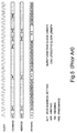
- Fig. 5 shows access timing in the above operation.
- Fig. 5 shows an example of access operation on the condition that the burst length is 8 clock length, and a COLUMN address strobe (CAS) latency is 2 clock length.
- a combination of control signals for execution of processing is called a command.
- data on the data bus (D) is stored into the memory upon setting of writing (WR) command, on the other hand, upon reading (RD) of information from the memory, after the execution of command, the information is outputted onto the data bus with delay of clock length of the CAS latency. Accordingly, a period where the data bus is not used exists between the writing processing and the reading processing.
- the present invention has its object to provide an SDRAM memory access method to reduce an idle period, where a data bus is not used, caused by access to a memory area with a different ROW address, by reservation registration and preparation for the execution of command to be executed next during a burst data writing/reading cycle, so as to increase data transfer efficiency and realize high speed burst data transfer, and to provide a simple memory interface.
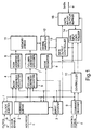
- Fig. 1 is a block diagram of an SDRAM of a memory access system according to an embodiment of the present invention.
- the memory access system has a clock buffer 1 which controls supply of clock signal a , inputted form the outside and delivers the signal to respective elements of the SDRAM so as to drive the elements, an address buffer 2 in which an address signal c or operation start pre-setting signal in synchronization with a rise of a clock signal outputted from the clock buffer 1, a burst counter 3 which generates a burst length address set upon burst data transfer to the outside, a ROW address register 4 in which a ROW address outputted from the address buffer 2 is latched for timing adjustment, a COLUMN address register 5 in which a COLUMN address outputted from the address buffer 2 is latched for timing adjustment, a ROW address decoder 6 which decodes the ROW address outputted from the ROW address register 4, a COLUMN address decoder 7 which decodes the COLUMN address outputted from the COLUMN address register 5, a mode register 8 in which an operation mode of the SDRAM is set, a command decoder 9 which
- the SDRAM Before the SDRAM is used, its operation mode is set in the mode register 8 by address input. The setting is held until the mode is re-set or the power is turned off. The mode set in the mode register 8 is transmitted to the controller 10, and the controller 10 generates a control signal based on the mode and controls the respective elements of the SDRAM.
- the command decoder 9 Upon input of address a and the control signal d, the command decoder 9 interprets the command type of the control signal d, and the controller 10 generates a control signal in correspondence with the determined command and outputs the signal.
- Fig. 2 is a timing chart on the condition that the burst length is 8 clock length and the COLUMN address strobe (CAS) latency is 2 clock length.
- CAS COLUMN address strobe
- the command decoder 9 interprets the command as "ROW address setting (ACT)"
- the input address a is latched in the address buffer 2, and is outputted to the ROW address register 4.
- the command decoder 9 interprets the command as "writing (WR)” or “reading (RD)”
- the input address a is latched in the address buffer 2, and is outputted to the COLUMN address register 5.
- a writing (WR) command is inputted following the ROW address setting (ADT).
- the ROW address is outputted from the ROW address register 4 to the ROW address decoder 6 in synchronization with the COLUMN address inputted upon writing.
- the timing-adjusted ROW address and the COLUNN address select a memory cell designated by the ROW address decoder 6 and the COLUMN address decoder 7 from a memory array 11.
- the controller 10 prohibits output from the data output controller 13, and controls the dccc input controller 14 to receive the input data e through the data input/output buffer 15.
- the data e is stored from the data input controller 14 through the sense amplifier 12 into the selected memory cell in the memory array 11.
- the burst counter 3 When burst first access information is written and held, the burst counter 3 generates an address of memory location for holding the information. The generated address is latched in the COLUMN address register 5 at the next clock, and is outputted to the COLUMN address decoder 7. Then the data e inputted through the input/output buffer 15 is stored into the memory selected by the address from the memory array 11, as in the case of the first access. Third to eighth accesses, information can be written into the memory, as in the case of the first and second accesses.
- a new command is inputted during a writing cycle as shown in Fig. 3, the execution stops, however, in the present invention, after a predetermined period from the input of writing command, new input of a writing (WR) command, a reading (RD) command and a precharge (PRE) command are executed after the completion of execution of already being executed command. That is, if a command is newly inputted while a current command is executed, the next execution is reserved for the new command, and preparation is made for quickly executing the new command. Note that a burst transfer operation can be terminated by a burst stop (BST) command.
- BST burst stop
- a new reading (RD) command is inputted, and the next execution is reserved for the new command.
- the address inputted at the same time of the reading command is stored as a COLUMN address in the address buffer 2.
- the COLUMN address is timing adjusted by the COLUMN address register 5 with the ROW address, and outputted to the COLUMN address decoder 7. Then, a memory cell designated by the ROW address and the COLUMN address is selected from the memory array 11, and the stored information is read through the sense amplifier 12.
- the controller 10 controls the output from the data input controller 14 to high impedance based on the reading command, and controls the output from the data output controller 13 to output the output data from the sense amplifier 12 from the data input/output buffer 15.
- the burst transfer from the second access with the reading (RD) command is similarly processed.
- the execution of the input command is reserved, and the execution of the command is prepared by the completion of the currently-executed reading processing, and then sequentially executed after the completion of execution of the previous command.
- a memory cell in the memory array designated by the ROW address decoder 6 and the COLUMN address decoder 7 is selected, from the LOW address and the COLUMN address timing adjusted by the ROW address register 4 and the COLUMN address register 5.
- the data input controller 14 and the data output controller 13 are controlled by a control signal generated by the controller 10 in accordance with a command from the command decoder 9. If the command is "writing”, the data e inputted through the data input/output buffer 15 is stored into the selected memory cell in the memory array 11. Further, if the command is "reading", information is read from the selected memory cell in the memory array 11, and outputted from the data input/output buffer 15 through the sense amplifier 12 by controlling the output of the data output controller 13.
- This operation may be realized by providing the mode register 8 with control information, and switching the operation of the conventional SDRAM with that of the embodiment of the present invention by the control information set in the mode register 8.
- mode setting if the latency of writing is different from that of reading, the mode setting information is inputted into the controller 10, and the controller 10 time controls the input controller 14 and the output controller 13 so as to bring the faster latency into correspondence with the slower latency.
- reservation registration and execution preparation are made for a command to be executed next, and after the currently-executed cycle, the reserve-registered command is executed. This reduces an idle period where the data bus is not used upon access to a memory area with a different ROW address, and realizes a high data transfer speed.
- an idle period where the data bus is not used is reduced, and a high data transfer speed can be attained. Further, latency of writing and that of reading different from each other are brought into correspondence, and upon execution of reading from writing, the idle period where the data bus is not effectively used is solved, and the memory data interface can be simplified.
Landscapes
- Engineering & Computer Science (AREA)
- Theoretical Computer Science (AREA)
- Physics & Mathematics (AREA)
- General Engineering & Computer Science (AREA)
- General Physics & Mathematics (AREA)
- Dram (AREA)
- Memory System (AREA)
Abstract
Description
Claims (7)
- A memory access method comprising:a step of discriminating an input command;a step of, after discrimination of ROW address setting from said command, holding an input address as a ROW address for a predetermined period;a step of, if writing or reading is discriminated from said command, holding an input address as a COLUMN address for a predetermined period; anda step of selecting a memory cell based on the held ROW and COLUMN addresses.
- The memory access method according to claim 1, further comprising a step of, when writing is performed in accordance with said command, inputting a new reading command and reserving execution of the newly input command during a writing cycle.
- The memory access method according to claim 1 or 2, further comprising a step of, if latency of the writing and that of the reading have different values, adjusting a faster latency to a slower latency.
- The memory access method according to claim 1, 2 or 3 wherein the memory is a synchronous DRAM (Dynamic Random Access Memory).
- A memory access system comprising:first holding means for, after discrimination of ROW address setting from said command, holding an input address as a ROW address for a predetermined period;second holding means for, if writing or reading is discriminated from said command, holding an input address as a COLUMN address for a predetermined period; andselection means for selecting a memory cell based on the held ROW and COLUMN addresses.
- The memory access system according to claim 5, wherein the memory is a synchronous DRAM (Dynamic Random Access Memory).
- A synchronous DRAM (Dynamic Random Access Memory) access system comprising:an address buffer that reads an address signal or operation start pre-setting signal from outside in synchronization with an input clock;a burst counter that generates an address of a burst length set upon burst data transfer with the outside;a ROW address register that performs timing adjustment by latching a ROW address outputted from said address buffer;a COLUMN address register that performs timing adjustment by latching a COLUMN address outputted from said address buffer;a ROW address decoder that decodes the ROW address outputted from said ROW address register;a COLUMN address decoder that decodes the COLUMN address outputted from said COLUMN address register;a mode register that sets an operation mode of the DRAM by said operation start pre-setting signal;a command decoder that interprets and discriminates a command by a control signal from the outside;a controller that controls an overall operation of the DRAM in accordance with a command interpretation and discrimination result signal outputted from said command decoder;a memory array having a large number of memory cells for holding data for burst data transfer with the outside;a data output controller, controlled by a control signal from said controller, that controls output of said data from said memory array;a data input/output buffer for transmission/reception of said data between the outside and inside, in synchronization with said input clock; anda data input controller, controlled by the control signal outputted from said controller, that controls input of said data from said input/output buffer.
Applications Claiming Priority (2)
| Application Number | Priority Date | Filing Date | Title |
|---|---|---|---|
| JP11207126A JP2001035158A (en) | 1999-07-22 | 1999-07-22 | Method and system for accessing memory |
| JP20712699 | 1999-07-22 |
Publications (2)
| Publication Number | Publication Date |
|---|---|
| EP1071095A2 true EP1071095A2 (en) | 2001-01-24 |
| EP1071095A3 EP1071095A3 (en) | 2001-04-04 |
Family
ID=16534637
Family Applications (1)
| Application Number | Title | Priority Date | Filing Date |
|---|---|---|---|
| EP00114976A Withdrawn EP1071095A3 (en) | 1999-07-22 | 2000-07-20 | Memory acces method and system |
Country Status (4)
| Country | Link |
|---|---|
| US (1) | US6469940B1 (en) |
| EP (1) | EP1071095A3 (en) |
| JP (1) | JP2001035158A (en) |
| KR (1) | KR100375895B1 (en) |
Cited By (2)
| Publication number | Priority date | Publication date | Assignee | Title |
|---|---|---|---|---|
| US20110016291A1 (en) * | 2009-07-17 | 2011-01-20 | Macronix International Co., Ltd. | Serial Memory Interface for Extended Address Space |
| CN107545919A (en) * | 2016-06-23 | 2018-01-05 | 联发科技股份有限公司 | Dynamic random access memory, and access method and operation method thereof |
Families Citing this family (10)
| Publication number | Priority date | Publication date | Assignee | Title |
|---|---|---|---|---|
| KR100442426B1 (en) * | 2000-12-27 | 2004-07-30 | 엘지전자 주식회사 | Memory control apparatus |
| US6987822B2 (en) * | 2001-03-13 | 2006-01-17 | Micron Technology, Inc. | Circuit and method for reducing noise interference in digital differential input receivers |
| DE10219370A1 (en) * | 2002-04-30 | 2003-11-20 | Infineon Technologies Ag | Reading data with specific burst length out of semiconductor memory takes over first address part from memory cell address bus and transmits read-out instruction to instruction bus of memory |
| KR100452332B1 (en) * | 2002-10-17 | 2004-10-12 | 한국전자통신연구원 | Method for improving data read and write speed |
| US6931479B2 (en) * | 2003-03-04 | 2005-08-16 | Micron Technology, Inc. | Method and apparatus for multi-functional inputs of a memory device |
| KR100592188B1 (en) | 2003-10-20 | 2006-06-23 | (주)씨앤에스 테크놀로지 | Data interface device for SDRAM access |
| CN100395696C (en) * | 2006-08-11 | 2008-06-18 | 华为技术有限公司 | Static memory interface device and data transmission method thereof |
| TWI311326B (en) * | 2006-12-01 | 2009-06-21 | Realtek Semiconductor Corp | Memory controller and signal synchronizing method thereof |
| JP2008140220A (en) * | 2006-12-04 | 2008-06-19 | Nec Corp | Semiconductor device |
| KR101191942B1 (en) | 2007-10-10 | 2012-10-17 | 삼성전자주식회사 | Semiconductor memory device and command input method of the semiconductor memory device |
Family Cites Families (9)
| Publication number | Priority date | Publication date | Assignee | Title |
|---|---|---|---|---|
| JPS61214298A (en) * | 1985-03-20 | 1986-09-24 | Toshiba Corp | Semiconductor memory with error correcting function |
| JP3275554B2 (en) * | 1994-08-09 | 2002-04-15 | ヤマハ株式会社 | Semiconductor storage device |
| US5655105A (en) | 1995-06-30 | 1997-08-05 | Micron Technology, Inc. | Method and apparatus for multiple latency synchronous pipelined dynamic random access memory |
| US5748551A (en) | 1995-12-29 | 1998-05-05 | Micron Technology, Inc. | Memory device with multiple internal banks and staggered command execution |
| JPH10233091A (en) | 1997-02-21 | 1998-09-02 | Hitachi Ltd | Semiconductor storage device and data processing device |
| JP3267259B2 (en) | 1998-12-22 | 2002-03-18 | 日本電気株式会社 | Semiconductor storage device |
| JP3957421B2 (en) | 1999-02-10 | 2007-08-15 | エルピーダメモリ株式会社 | Semiconductor memory device |
| KR100304705B1 (en) * | 1999-03-03 | 2001-10-29 | 윤종용 | SDRAM having posted CAS latency and CAS latency control method therefor |
| JP2000330967A (en) * | 1999-05-25 | 2000-11-30 | Nec Corp | Semiconductor memory and its manufacture |
-
1999
- 1999-07-22 JP JP11207126A patent/JP2001035158A/en active Pending
-
2000
- 2000-07-18 US US09/618,282 patent/US6469940B1/en not_active Expired - Fee Related
- 2000-07-20 EP EP00114976A patent/EP1071095A3/en not_active Withdrawn
- 2000-07-22 KR KR10-2000-0042125A patent/KR100375895B1/en not_active Expired - Fee Related
Cited By (3)
| Publication number | Priority date | Publication date | Assignee | Title |
|---|---|---|---|---|
| US20110016291A1 (en) * | 2009-07-17 | 2011-01-20 | Macronix International Co., Ltd. | Serial Memory Interface for Extended Address Space |
| US8677100B2 (en) * | 2009-07-17 | 2014-03-18 | Macronix International Co., Ltd. | Serial memory interface for extended address space |
| CN107545919A (en) * | 2016-06-23 | 2018-01-05 | 联发科技股份有限公司 | Dynamic random access memory, and access method and operation method thereof |
Also Published As
| Publication number | Publication date |
|---|---|
| EP1071095A3 (en) | 2001-04-04 |
| KR20010029985A (en) | 2001-04-16 |
| KR100375895B1 (en) | 2003-03-15 |
| US6469940B1 (en) | 2002-10-22 |
| JP2001035158A (en) | 2001-02-09 |
Similar Documents
| Publication | Publication Date | Title |
|---|---|---|
| US7782683B2 (en) | Multi-port memory device for buffering between hosts and non-volatile memory devices | |
| US6421274B1 (en) | Semiconductor memory device and reading and writing method thereof | |
| US5903514A (en) | Multi-bank synchronous semiconductor memory device | |
| US7133996B2 (en) | Memory device and internal control method therefor | |
| US20040095818A1 (en) | Memory controller and data processing system | |
| US20020110037A1 (en) | Dram interface circuit providing continuous access across row boundaries | |
| JP2001052479A (en) | Memory device | |
| EP1071095A2 (en) | Memory acces method and system | |
| US20030128593A1 (en) | Semiconductor storage apparatus | |
| JPH05210567A (en) | Memory device and data read/write method of memory | |
| JPH0684351A (en) | Clock synchronous semiconductor memory device and access method thereof | |
| JP2007220271A (en) | Burst read circuit and burst data output method for semiconductor memory device | |
| US6091667A (en) | Semiconductor memory device and a data reading method and a data writing method therefor | |
| KR101027181B1 (en) | Memory control method and memory system | |
| CN1707694B (en) | Memory Controller for Multithreaded Pipelined Bus Systems | |
| EP1248267A2 (en) | Semiconductor memory device and information processing system | |
| US7313046B2 (en) | Semiconductor memory devices in which the number of memory banks to be refreshed may be changed and methods of operating the same | |
| KR100648292B1 (en) | Auto Dual Buffering Memory Device | |
| US6545932B1 (en) | SDRAM and method for data accesses of SDRAM | |
| US6029235A (en) | Automatic reloading of serial read pipeline on last bit transfers to serial access memory | |
| US6069639A (en) | Video camera system and semiconductor image memory circuit applied to it | |
| US6556484B2 (en) | Plural line buffer type memory LSI | |
| EP1416494A2 (en) | Semiconductor memory capable of performing high-speed processing | |
| US7111122B2 (en) | Access circuit with various access data units | |
| US20070073961A1 (en) | Memory controller |
Legal Events
| Date | Code | Title | Description |
|---|---|---|---|
| PUAI | Public reference made under article 153(3) epc to a published international application that has entered the european phase |
Free format text: ORIGINAL CODE: 0009012 |
|
| AK | Designated contracting states |
Kind code of ref document: A2 Designated state(s): DE GB |
|
| AX | Request for extension of the european patent |
Free format text: AL;LT;LV;MK;RO;SI |
|
| PUAL | Search report despatched |
Free format text: ORIGINAL CODE: 0009013 |
|
| AK | Designated contracting states |
Kind code of ref document: A3 Designated state(s): AT BE CH CY DE DK ES FI FR GB GR IE IT LI LU MC NL PT SE |
|
| AX | Request for extension of the european patent |
Free format text: AL;LT;LV;MK;RO;SI |
|
| RIC1 | Information provided on ipc code assigned before grant |
Free format text: 7G 11C 7/22 A, 7G 11C 7/10 B, 7G 11C 11/407 B, 7G 11C 8/00 B |
|
| 17P | Request for examination filed |
Effective date: 20010220 |
|
| AKX | Designation fees paid |
Free format text: DE GB |
|
| STAA | Information on the status of an ep patent application or granted ep patent |
Free format text: STATUS: THE APPLICATION HAS BEEN WITHDRAWN |
|
| 18W | Application withdrawn |
Effective date: 20030616 |