EP1071070A2 - Low current drive of light emitting device - Google Patents
Low current drive of light emitting device Download PDFInfo
- Publication number
- EP1071070A2 EP1071070A2 EP00112843A EP00112843A EP1071070A2 EP 1071070 A2 EP1071070 A2 EP 1071070A2 EP 00112843 A EP00112843 A EP 00112843A EP 00112843 A EP00112843 A EP 00112843A EP 1071070 A2 EP1071070 A2 EP 1071070A2
- Authority
- EP
- European Patent Office
- Prior art keywords
- light emitting
- emitting device
- current source
- voltage
- column
- Prior art date
- Legal status (The legal status is an assumption and is not a legal conclusion. Google has not performed a legal analysis and makes no representation as to the accuracy of the status listed.)
- Granted
Links
- 239000003990 capacitor Substances 0.000 claims description 10
- 238000000034 method Methods 0.000 claims 5
- 238000007599 discharging Methods 0.000 claims 1
- 230000004913 activation Effects 0.000 description 3
- 238000010586 diagram Methods 0.000 description 2
- 238000005516 engineering process Methods 0.000 description 2
- 239000011159 matrix material Substances 0.000 description 1
- 230000007704 transition Effects 0.000 description 1
Images



Classifications
-
- G—PHYSICS
- G09—EDUCATION; CRYPTOGRAPHY; DISPLAY; ADVERTISING; SEALS
- G09G—ARRANGEMENTS OR CIRCUITS FOR CONTROL OF INDICATING DEVICES USING STATIC MEANS TO PRESENT VARIABLE INFORMATION
- G09G3/00—Control arrangements or circuits, of interest only in connection with visual indicators other than cathode-ray tubes
- G09G3/20—Control arrangements or circuits, of interest only in connection with visual indicators other than cathode-ray tubes for presentation of an assembly of a number of characters, e.g. a page, by composing the assembly by combination of individual elements arranged in a matrix no fixed position being assigned to or needed to be assigned to the individual characters or partial characters
- G09G3/22—Control arrangements or circuits, of interest only in connection with visual indicators other than cathode-ray tubes for presentation of an assembly of a number of characters, e.g. a page, by composing the assembly by combination of individual elements arranged in a matrix no fixed position being assigned to or needed to be assigned to the individual characters or partial characters using controlled light sources
- G09G3/30—Control arrangements or circuits, of interest only in connection with visual indicators other than cathode-ray tubes for presentation of an assembly of a number of characters, e.g. a page, by composing the assembly by combination of individual elements arranged in a matrix no fixed position being assigned to or needed to be assigned to the individual characters or partial characters using controlled light sources using electroluminescent panels
- G09G3/32—Control arrangements or circuits, of interest only in connection with visual indicators other than cathode-ray tubes for presentation of an assembly of a number of characters, e.g. a page, by composing the assembly by combination of individual elements arranged in a matrix no fixed position being assigned to or needed to be assigned to the individual characters or partial characters using controlled light sources using electroluminescent panels semiconductive, e.g. using light-emitting diodes [LED]
- G09G3/3208—Control arrangements or circuits, of interest only in connection with visual indicators other than cathode-ray tubes for presentation of an assembly of a number of characters, e.g. a page, by composing the assembly by combination of individual elements arranged in a matrix no fixed position being assigned to or needed to be assigned to the individual characters or partial characters using controlled light sources using electroluminescent panels semiconductive, e.g. using light-emitting diodes [LED] organic, e.g. using organic light-emitting diodes [OLED]
- G09G3/3216—Control arrangements or circuits, of interest only in connection with visual indicators other than cathode-ray tubes for presentation of an assembly of a number of characters, e.g. a page, by composing the assembly by combination of individual elements arranged in a matrix no fixed position being assigned to or needed to be assigned to the individual characters or partial characters using controlled light sources using electroluminescent panels semiconductive, e.g. using light-emitting diodes [LED] organic, e.g. using organic light-emitting diodes [OLED] using a passive matrix
-
- G—PHYSICS
- G09—EDUCATION; CRYPTOGRAPHY; DISPLAY; ADVERTISING; SEALS
- G09G—ARRANGEMENTS OR CIRCUITS FOR CONTROL OF INDICATING DEVICES USING STATIC MEANS TO PRESENT VARIABLE INFORMATION
- G09G3/00—Control arrangements or circuits, of interest only in connection with visual indicators other than cathode-ray tubes
- G09G3/20—Control arrangements or circuits, of interest only in connection with visual indicators other than cathode-ray tubes for presentation of an assembly of a number of characters, e.g. a page, by composing the assembly by combination of individual elements arranged in a matrix no fixed position being assigned to or needed to be assigned to the individual characters or partial characters
- G09G3/22—Control arrangements or circuits, of interest only in connection with visual indicators other than cathode-ray tubes for presentation of an assembly of a number of characters, e.g. a page, by composing the assembly by combination of individual elements arranged in a matrix no fixed position being assigned to or needed to be assigned to the individual characters or partial characters using controlled light sources
- G09G3/30—Control arrangements or circuits, of interest only in connection with visual indicators other than cathode-ray tubes for presentation of an assembly of a number of characters, e.g. a page, by composing the assembly by combination of individual elements arranged in a matrix no fixed position being assigned to or needed to be assigned to the individual characters or partial characters using controlled light sources using electroluminescent panels
- G09G3/32—Control arrangements or circuits, of interest only in connection with visual indicators other than cathode-ray tubes for presentation of an assembly of a number of characters, e.g. a page, by composing the assembly by combination of individual elements arranged in a matrix no fixed position being assigned to or needed to be assigned to the individual characters or partial characters using controlled light sources using electroluminescent panels semiconductive, e.g. using light-emitting diodes [LED]
- G09G3/3208—Control arrangements or circuits, of interest only in connection with visual indicators other than cathode-ray tubes for presentation of an assembly of a number of characters, e.g. a page, by composing the assembly by combination of individual elements arranged in a matrix no fixed position being assigned to or needed to be assigned to the individual characters or partial characters using controlled light sources using electroluminescent panels semiconductive, e.g. using light-emitting diodes [LED] organic, e.g. using organic light-emitting diodes [OLED]
- G09G3/3275—Details of drivers for data electrodes
- G09G3/3283—Details of drivers for data electrodes in which the data driver supplies a variable data current for setting the current through, or the voltage across, the light-emitting elements
-
- G—PHYSICS
- G09—EDUCATION; CRYPTOGRAPHY; DISPLAY; ADVERTISING; SEALS
- G09G—ARRANGEMENTS OR CIRCUITS FOR CONTROL OF INDICATING DEVICES USING STATIC MEANS TO PRESENT VARIABLE INFORMATION
- G09G2310/00—Command of the display device
- G09G2310/02—Addressing, scanning or driving the display screen or processing steps related thereto
- G09G2310/0243—Details of the generation of driving signals
- G09G2310/0248—Precharge or discharge of column electrodes before or after applying exact column voltages
-
- G—PHYSICS
- G09—EDUCATION; CRYPTOGRAPHY; DISPLAY; ADVERTISING; SEALS
- G09G—ARRANGEMENTS OR CIRCUITS FOR CONTROL OF INDICATING DEVICES USING STATIC MEANS TO PRESENT VARIABLE INFORMATION
- G09G2310/00—Command of the display device
- G09G2310/02—Addressing, scanning or driving the display screen or processing steps related thereto
- G09G2310/0243—Details of the generation of driving signals
- G09G2310/0251—Precharge or discharge of pixel before applying new pixel voltage
-
- G—PHYSICS
- G09—EDUCATION; CRYPTOGRAPHY; DISPLAY; ADVERTISING; SEALS
- G09G—ARRANGEMENTS OR CIRCUITS FOR CONTROL OF INDICATING DEVICES USING STATIC MEANS TO PRESENT VARIABLE INFORMATION
- G09G2330/00—Aspects of power supply; Aspects of display protection and defect management
- G09G2330/02—Details of power systems and of start or stop of display operation
-
- G—PHYSICS
- G09—EDUCATION; CRYPTOGRAPHY; DISPLAY; ADVERTISING; SEALS
- G09G—ARRANGEMENTS OR CIRCUITS FOR CONTROL OF INDICATING DEVICES USING STATIC MEANS TO PRESENT VARIABLE INFORMATION
- G09G2330/00—Aspects of power supply; Aspects of display protection and defect management
- G09G2330/02—Details of power systems and of start or stop of display operation
- G09G2330/028—Generation of voltages supplied to electrode drivers in a matrix display other than LCD
-
- G—PHYSICS
- G09—EDUCATION; CRYPTOGRAPHY; DISPLAY; ADVERTISING; SEALS
- G09G—ARRANGEMENTS OR CIRCUITS FOR CONTROL OF INDICATING DEVICES USING STATIC MEANS TO PRESENT VARIABLE INFORMATION
- G09G3/00—Control arrangements or circuits, of interest only in connection with visual indicators other than cathode-ray tubes
- G09G3/20—Control arrangements or circuits, of interest only in connection with visual indicators other than cathode-ray tubes for presentation of an assembly of a number of characters, e.g. a page, by composing the assembly by combination of individual elements arranged in a matrix no fixed position being assigned to or needed to be assigned to the individual characters or partial characters
- G09G3/2007—Display of intermediate tones
- G09G3/2014—Display of intermediate tones by modulation of the duration of a single pulse during which the logic level remains constant
Definitions
- a waveform 66 represents a signal placed on column line 20.
- Column data 67 indicates whether a light emitting device in an activated row will be on or off during a particular time period. "ON” indicates that a light emitting device in the column is to be turned on. “OFF” indicates that no light emitting device in the column is to be turned on.
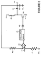
- column line 20 When light emitting device 23 is turned on, column line 20 is at the Vf or greater and row line 21 is connected to ground 11. This results in charging capacitance 24. Once the voltage across capacitance 24 is greater than Vf, diode 25 generates light. Any current that travels through the capacitance of other light emitting devices in the column travels to high voltage line 10 and back into capacitor 52 of the high voltage multiplier shown in Figure 2.
Landscapes
- Engineering & Computer Science (AREA)
- Physics & Mathematics (AREA)
- Computer Hardware Design (AREA)
- General Physics & Mathematics (AREA)
- Theoretical Computer Science (AREA)
- Electroluminescent Light Sources (AREA)
- Control Of Indicators Other Than Cathode Ray Tubes (AREA)
- Control Of El Displays (AREA)
- Led Devices (AREA)
- Electronic Switches (AREA)
Abstract
Description
Claims (10)
- Control circuitry for an array of light emitting devices (23,27), circuitry comprising:a first column line (20) connected to each light emitting device (23,27) in a column of light emitting devices (23,27);first column circuitry comprising:wherein when a first light emitting device (23,27) from the column of light emitting devices (23,27) is to be turned on, the first current source (15) is turned on until a voltage on the first column line (20) is equal to a predetermined voltage, then the first current source (15) is turned off and the second current source (20) supplies current sufficient to cause the first light emitting device (23,27) to emit light to a first brightness level.a first current source (15) connected to the first column line (20), anda second current source (20) connected to the first column line (20) ;
- Control circuitry as in claim 1, wherein the first column circuitry additionally comprises:a switch (17) connected to the first column line (20) and to an output capacitance (18) of a low voltage power supply;
wherein when the voltage on the first column line (20) is to be discharged, the switch (17) is turned on allowing the voltage to be discharged to the output capacitance (18) of the low voltage power supply. - Control circuitry as in any previous claim additionally comprising:.a second column line (120);second column circuitry comprising:a third current source (115) connected to the second column line (120), anda fourth current source (114) connected to the second column line (120).
- Control circuitry as in claim 3 additionally comprising:a capacitance (221);a fifth current source (215) which charges the capacitance (221),a comparator (216) which compares a reference voltage on a reference voltage line (12) to a voltage across the capacitance (221), the comparator (216) controlling the first current source (15), the third current source (115) and the fifth current source (215)
wherein the comparator (216) turns off the first current source (15) when the voltage across the capacitance (221) is equal to the reference voltage. - Control circuitry as in any previous claim additionally comprising:a power supply having an output on which is placed a signal with a voltage high enough to turn on light emitting devices (23,27) from the array of light emitting devices (23,27);a plurality of row lines (21,22) ;a plurality of switches (33-36), each switch (33-36) connected to an associated row line from the plurality of row Lines (21,22), each switch (33-36) connecting the associated row line (21,22) to either the output of the power supply (10) or to ground (11).
- A method for controlling an array of light emitting devices (23,27), circuitry comprising the following steps:(a) when a first light emitting device (23,27) from a column of light emitting devices (23,27) is to be turned on, charging capacitance (24,28) of the first light emitting diode (23,27) utilizing a first current source (15) until a voltage across the first light emitting device (23,27) is equal to a predetermined voltage;(b) when the voltage across the first light emitting device (23,27) is equal to the predetermined voltage, shutting off the first current source (15); and,(c) utilizing a second current source (20) to supply current sufficient to cause the first light emitting device (23,27) to emit light to a first brightness level.
- A method as in claim 6, additionally comprising the following step:(d) when the first light emitting device (23,27) is to be turned off, discharging the capacitance (24,28) of the first light emitting device (23,27) to output capacitance (18) of a low voltage power supply.
- A method as in claim 6 or 7, wherein step (a) includes the following substeps:(a.2) while charging the capacitance (24,28) of the first light emitting device (23,27) also charging a mirror capacitance (221) using a third current source (215);(a.1) comparing a reference voltage on a reference voltage line (12) to the voltage across the mirror capacitance (221).
- A method as in claim 6, 7 or 8 additionally comprising the following step:(d) when the first light emitting device (23,27) is turned off, reverse biasing the first light emitting device (23,27) such that charge stored in the light emitting device (23,27) flows back into a capacitor (18) on a voltage supply.
- A method as in claim 6, 7, 8 or 9 wherein the array of light emitting devices (23,27) is an array of organic light emitting diodes.
Applications Claiming Priority (2)
| Application Number | Priority Date | Filing Date | Title |
|---|---|---|---|
| US09/357,786 US6191534B1 (en) | 1999-07-21 | 1999-07-21 | Low current drive of light emitting devices |
| US357786 | 1999-07-21 |
Publications (4)
| Publication Number | Publication Date |
|---|---|
| EP1071070A2 true EP1071070A2 (en) | 2001-01-24 |
| EP1071070A3 EP1071070A3 (en) | 2002-01-16 |
| EP1071070B1 EP1071070B1 (en) | 2005-04-27 |
| EP1071070B9 EP1071070B9 (en) | 2005-07-13 |
Family
ID=23407014
Family Applications (1)
| Application Number | Title | Priority Date | Filing Date |
|---|---|---|---|
| EP00112843A Expired - Lifetime EP1071070B9 (en) | 1999-07-21 | 2000-06-17 | Low current drive of light emitting device |
Country Status (4)
| Country | Link |
|---|---|
| US (1) | US6191534B1 (en) |
| EP (1) | EP1071070B9 (en) |
| JP (1) | JP4012359B2 (en) |
| DE (1) | DE60019689T2 (en) |
Cited By (25)
| Publication number | Priority date | Publication date | Assignee | Title |
|---|---|---|---|---|
| EP1282104A1 (en) * | 2001-08-02 | 2003-02-05 | Seiko Epson Corporation | Driving of data lines in active matrix display device and display device |
| WO2003033749A1 (en) * | 2001-10-19 | 2003-04-24 | Clare Micronix Integrated Syst | Matrix element precharge voltage adjusting apparatus and method |
| SG98054A1 (en) * | 2001-05-31 | 2003-08-20 | Sony Corp | Active matrix type display apparatus, active matrix type organic electroluminescence display apparatus, and driveing methods thereof |
| WO2003098974A1 (en) * | 2002-05-16 | 2003-11-27 | Koninklijke Philips Electronics N.V. | Led capacitance discharge with limited current |
| WO2003038792A3 (en) * | 2001-10-30 | 2003-12-04 | Three Five Systems Inc | Controlling data dependence and cross-talk between display elements |
| WO2002091342A3 (en) * | 2001-05-09 | 2004-01-22 | Clare Micronix Integrated Syst | Matrix element voltage sensing for determining a precharge voltage |
| WO2003034390A3 (en) * | 2001-10-19 | 2004-03-18 | Clare Micronix Integrated Syst | Precharge circuit and method for passive matrix oled display |
| EP1274065A3 (en) * | 2001-07-06 | 2004-03-24 | Lg Electronics Inc. | Circuit and method for driving display of current driven type |
| WO2002091341A3 (en) * | 2001-05-09 | 2004-04-08 | Clare Micronix Integrated Syst | Apparatus and method of periodic voltage sensing for control of precharging of a pixel |
| WO2004047065A1 (en) * | 2002-11-15 | 2004-06-03 | Koninklijke Philips Electronics N.V. | Display device with pre-charging arrangement |
| WO2004006218A3 (en) * | 2002-07-09 | 2004-07-08 | Casio Computer Co Ltd | Driving device, display apparatus using the same, and driving method therefor |
| WO2004030042A3 (en) * | 2002-09-27 | 2004-09-23 | Tdk Semiconductor Corp | Method and apparatus for current driving of light emitting polymer displays |
| EP1553551A3 (en) * | 2004-01-10 | 2005-09-21 | Lg Electronics Inc. | Apparatus and method for operating flat panel display |
| SG120889A1 (en) * | 2001-09-28 | 2006-04-26 | Semiconductor Energy Lab | A light emitting device and electronic apparatus using the same |
| SG120888A1 (en) * | 2001-09-28 | 2006-04-26 | Semiconductor Energy Lab | A light emitting device and electronic apparatus using the same |
| US7079130B2 (en) | 2001-05-09 | 2006-07-18 | Clare Micronix Integrated Systems, Inc. | Method for periodic element voltage sensing to control precharge |
| US7079131B2 (en) | 2001-05-09 | 2006-07-18 | Clare Micronix Integrated Systems, Inc. | Apparatus for periodic element voltage sensing to control precharge |
| CN100370502C (en) * | 2001-09-21 | 2008-02-20 | 株式会社半导体能源研究所 | Light emitting device, light emitting device driving method, and electronic apparatus |
| EP1291839A3 (en) * | 2001-09-05 | 2008-04-09 | Nec Corporation | Circuit for and method of driving current-driven device |
| CN100410992C (en) * | 2001-08-02 | 2008-08-13 | 精工爱普生株式会社 | Electro-optical device and driving method thereof |
| US7663576B2 (en) | 2004-07-14 | 2010-02-16 | Semiconductor Energy Laboratory Co., Ltd. | Video data correction circuit, control circuit of display device, and display device and electronic apparatus incorporating the same |
| WO2010018380A1 (en) * | 2008-08-15 | 2010-02-18 | Cambridge Display Technology Limited | Active matrix displays |
| US7839365B2 (en) | 2002-09-04 | 2010-11-23 | Koninklijke Philips Electronics N.V. | Control of current supplied by a transistor to a pixel in an electroluminescent display device |
| US8098028B2 (en) | 2006-07-11 | 2012-01-17 | Austriamicrosystems Ag | Control circuit and method for controlling LEDs |
| US8350785B2 (en) | 2003-09-12 | 2013-01-08 | Semiconductor Energy Laboratory Co., Ltd. | Semiconductor device and driving method of the same |
Families Citing this family (17)
| Publication number | Priority date | Publication date | Assignee | Title |
|---|---|---|---|---|
| WO2001054107A1 (en) * | 2000-01-21 | 2001-07-26 | Emagin Corporation | Gray scale pixel driver for electronic display and method of operation therefor |
| TW461002B (en) * | 2000-06-05 | 2001-10-21 | Ind Tech Res Inst | Testing apparatus and testing method for organic light emitting diode array |
| JP2002076352A (en) * | 2000-08-31 | 2002-03-15 | Semiconductor Energy Lab Co Ltd | Display device and manufacturing method thereof |
| JP3989718B2 (en) * | 2001-01-18 | 2007-10-10 | シャープ株式会社 | Memory integrated display element |
| JP3788916B2 (en) * | 2001-03-30 | 2006-06-21 | 株式会社日立製作所 | Light-emitting display device |
| US20030169241A1 (en) * | 2001-10-19 | 2003-09-11 | Lechevalier Robert E. | Method and system for ramp control of precharge voltage |
| US7034781B2 (en) * | 2003-02-14 | 2006-04-25 | Elantec Semiconductor Inc. | Methods and systems for driving displays including capacitive display elements |
| CN100356416C (en) * | 2003-04-28 | 2007-12-19 | 统宝光电股份有限公司 | Method and system for testing driving circuit of active light-emitting display technology |
| US20050007321A1 (en) * | 2003-06-30 | 2005-01-13 | Schuler Jeffrey A. | Reduced reverse bias in organic light emitting diode displays |
| JP4758085B2 (en) * | 2003-09-12 | 2011-08-24 | 株式会社半導体エネルギー研究所 | Semiconductor device and electronic equipment |
| JP4565873B2 (en) * | 2004-03-29 | 2010-10-20 | 東北パイオニア株式会社 | Luminescent display panel |
| KR101085911B1 (en) * | 2004-07-30 | 2011-11-23 | 매그나칩 반도체 유한회사 | Organic light emitting device |
| KR100769445B1 (en) * | 2006-06-05 | 2007-10-22 | 삼성에스디아이 주식회사 | Backlight drive system of liquid crystal display |
| US8928240B2 (en) * | 2011-08-16 | 2015-01-06 | Abl Ip Holding Llc | Method and system for driving organic LED's |
| DE102012105630B4 (en) | 2012-06-27 | 2023-04-20 | OSRAM Opto Semiconductors Gesellschaft mit beschränkter Haftung | Lighting arrangement with lighting device and method for operating a lighting device |
| CN110853570B (en) * | 2019-11-20 | 2021-11-02 | 北京集创北方科技股份有限公司 | LED display device and its driving method and chip |
| CN113571006A (en) * | 2020-04-29 | 2021-10-29 | 联咏科技股份有限公司 | Display device and driver thereof |
Family Cites Families (16)
| Publication number | Priority date | Publication date | Assignee | Title |
|---|---|---|---|---|
| US3763468A (en) * | 1971-10-01 | 1973-10-02 | Energy Conversion Devices Inc | Light emitting display array with non-volatile memory |
| US4366504A (en) * | 1977-10-07 | 1982-12-28 | Sharp Kabushiki Kaisha | Thin-film EL image display panel |
| US4731610A (en) * | 1986-01-21 | 1988-03-15 | Ovonic Imaging Systems, Inc. | Balanced drive electronic matrix system and method of operating the same |
| KR100288037B1 (en) * | 1992-09-14 | 2001-05-02 | 가나이 쓰도무 | Method of driving display device |
| JPH0869577A (en) * | 1994-08-30 | 1996-03-12 | Rohm Co Ltd | Driving controller |
| US5552677A (en) * | 1995-05-01 | 1996-09-03 | Motorola | Method and control circuit precharging a plurality of columns prior to enabling a row of a display |
| JPH08330070A (en) | 1995-05-29 | 1996-12-13 | Pioneer Electron Corp | Drive method for luminescent element |
| US5847516A (en) * | 1995-07-04 | 1998-12-08 | Nippondenso Co., Ltd. | Electroluminescent display driver device |
| US5767823A (en) * | 1995-10-05 | 1998-06-16 | Micron Display, Inc. | Method and apparatus for gray scale modulation of a matrix display |
| US5719589A (en) * | 1996-01-11 | 1998-02-17 | Motorola, Inc. | Organic light emitting diode array drive apparatus |
| JP3547561B2 (en) * | 1996-05-15 | 2004-07-28 | パイオニア株式会社 | Display device |
| US5684368A (en) * | 1996-06-10 | 1997-11-04 | Motorola | Smart driver for an array of LEDs |
| US5723950A (en) * | 1996-06-10 | 1998-03-03 | Motorola | Pre-charge driver for light emitting devices and method |
| US5923308A (en) * | 1996-11-12 | 1999-07-13 | Motorola, Inc. | Array of leds with active pull down shadow canceling circuitry |
| JP2879670B2 (en) * | 1997-03-28 | 1999-04-05 | 広島大学長 | Two-dimensional information processing device |
| US5998805A (en) * | 1997-12-11 | 1999-12-07 | Motorola, Inc. | Active matrix OED array with improved OED cathode |
-
1999
- 1999-07-21 US US09/357,786 patent/US6191534B1/en not_active Expired - Lifetime
-
2000
- 2000-06-17 EP EP00112843A patent/EP1071070B9/en not_active Expired - Lifetime
- 2000-06-17 DE DE60019689T patent/DE60019689T2/en not_active Expired - Lifetime
- 2000-07-18 JP JP2000217873A patent/JP4012359B2/en not_active Expired - Lifetime
Cited By (55)
| Publication number | Priority date | Publication date | Assignee | Title |
|---|---|---|---|---|
| WO2002091342A3 (en) * | 2001-05-09 | 2004-01-22 | Clare Micronix Integrated Syst | Matrix element voltage sensing for determining a precharge voltage |
| US7079131B2 (en) | 2001-05-09 | 2006-07-18 | Clare Micronix Integrated Systems, Inc. | Apparatus for periodic element voltage sensing to control precharge |
| US7079130B2 (en) | 2001-05-09 | 2006-07-18 | Clare Micronix Integrated Systems, Inc. | Method for periodic element voltage sensing to control precharge |
| WO2002091341A3 (en) * | 2001-05-09 | 2004-04-08 | Clare Micronix Integrated Syst | Apparatus and method of periodic voltage sensing for control of precharging of a pixel |
| SG98054A1 (en) * | 2001-05-31 | 2003-08-20 | Sony Corp | Active matrix type display apparatus, active matrix type organic electroluminescence display apparatus, and driveing methods thereof |
| US6975290B2 (en) | 2001-05-31 | 2005-12-13 | Sony Corporation | Active matrix type display apparatus, active matrix type organic electroluminescence display apparatus, and driving methods thereof |
| EP1274065A3 (en) * | 2001-07-06 | 2004-03-24 | Lg Electronics Inc. | Circuit and method for driving display of current driven type |
| US7466311B2 (en) | 2001-08-02 | 2008-12-16 | Seiko Epson Corporation | Driving of data lines used in unit circuit control |
| EP1282104A1 (en) * | 2001-08-02 | 2003-02-05 | Seiko Epson Corporation | Driving of data lines in active matrix display device and display device |
| US6989826B2 (en) | 2001-08-02 | 2006-01-24 | Seiko Epson Corporation | Driving of data lines used in unit circuit control |
| EP1494203A3 (en) * | 2001-08-02 | 2007-07-18 | Seiko Epson Corporation | Driving of data lines used in a control circuit of a display device |
| CN100410992C (en) * | 2001-08-02 | 2008-08-13 | 精工爱普生株式会社 | Electro-optical device and driving method thereof |
| EP1291839A3 (en) * | 2001-09-05 | 2008-04-09 | Nec Corporation | Circuit for and method of driving current-driven device |
| EP2157562A2 (en) | 2001-09-05 | 2010-02-24 | Nec Corporation | Circuit for and method of driving current-driven device |
| EP2157562A3 (en) * | 2001-09-05 | 2010-03-03 | Nec Corporation | Circuit for and method of driving current-driven device |
| CN100370502C (en) * | 2001-09-21 | 2008-02-20 | 株式会社半导体能源研究所 | Light emitting device, light emitting device driving method, and electronic apparatus |
| CN101232040B (en) * | 2001-09-21 | 2010-12-08 | 株式会社半导体能源研究所 | Light emitting device, method for driving light emitting device, and electronic device |
| US7586505B2 (en) | 2001-09-28 | 2009-09-08 | Semiconductor Energy Laboratory Co., Ltd. | Light emitting device and electronic apparatus using the same |
| SG120889A1 (en) * | 2001-09-28 | 2006-04-26 | Semiconductor Energy Lab | A light emitting device and electronic apparatus using the same |
| CN100370503C (en) * | 2001-09-28 | 2008-02-20 | 株式会社半导体能源研究所 | Light-emitting device and electronic equipment using said device |
| US7688291B2 (en) | 2001-09-28 | 2010-03-30 | Semiconductor Energy Laboratory Co., Ltd. | Light emitting device and electronic apparatus using the same |
| US7199771B2 (en) | 2001-09-28 | 2007-04-03 | Semiconductor Energy Laboratory Co., Ltd. | Light emitting device and electronic apparatus using the same |
| US7158157B2 (en) | 2001-09-28 | 2007-01-02 | Semiconductor Energy Laboratory Co., Ltd. | Light emitting device and electronic apparatus using the same |
| SG120888A1 (en) * | 2001-09-28 | 2006-04-26 | Semiconductor Energy Lab | A light emitting device and electronic apparatus using the same |
| US7126568B2 (en) | 2001-10-19 | 2006-10-24 | Clare Micronix Integrated Systems, Inc. | Method and system for precharging OLED/PLED displays with a precharge latency |
| WO2003033749A3 (en) * | 2001-10-19 | 2004-01-29 | Clare Micronix Integrated Syst | Matrix element precharge voltage adjusting apparatus and method |
| WO2003034384A3 (en) * | 2001-10-19 | 2003-12-18 | Clare Micronix Integrated Syst | Method and system for precharging oled/pled displays with a precharge latency |
| US7050024B2 (en) | 2001-10-19 | 2006-05-23 | Clare Micronix Integrated Systems, Inc. | Predictive control boost current method and apparatus |
| WO2003034383A3 (en) * | 2001-10-19 | 2003-08-21 | Clare Micronix Integrated Syst | Drive circuit for adaptive control of precharge current and method therefor |
| WO2003033749A1 (en) * | 2001-10-19 | 2003-04-24 | Clare Micronix Integrated Syst | Matrix element precharge voltage adjusting apparatus and method |
| WO2003034388A3 (en) * | 2001-10-19 | 2004-01-08 | Clare Micronix Integrated Syst | Circuit for predictive control of boost current in a passive matrix oled display and method therefor |
| US6995737B2 (en) | 2001-10-19 | 2006-02-07 | Clare Micronix Integrated Systems, Inc. | Method and system for adjusting precharge for consistent exposure voltage |
| WO2003034386A3 (en) * | 2001-10-19 | 2003-10-16 | Clare Micronix Integrated Syst | Method and system for ramp control of precharge voltage |
| US7019720B2 (en) | 2001-10-19 | 2006-03-28 | Clare Micronix Integrated Systems, Inc. | Adaptive control boost current method and apparatus |
| WO2003034390A3 (en) * | 2001-10-19 | 2004-03-18 | Clare Micronix Integrated Syst | Precharge circuit and method for passive matrix oled display |
| US6943500B2 (en) | 2001-10-19 | 2005-09-13 | Clare Micronix Integrated Systems, Inc. | Matrix element precharge voltage adjusting apparatus and method |
| WO2003034391A3 (en) * | 2001-10-19 | 2004-04-01 | Clare Micronix Integrated Syst | Method and system for adjusting the voltage of a precharge circuit |
| WO2003038792A3 (en) * | 2001-10-30 | 2003-12-04 | Three Five Systems Inc | Controlling data dependence and cross-talk between display elements |
| WO2003098974A1 (en) * | 2002-05-16 | 2003-11-27 | Koninklijke Philips Electronics N.V. | Led capacitance discharge with limited current |
| CN100530310C (en) * | 2002-05-16 | 2009-08-19 | 统宝光电股份有限公司 | LED capacitive discharge using limited current |
| WO2004006218A3 (en) * | 2002-07-09 | 2004-07-08 | Casio Computer Co Ltd | Driving device, display apparatus using the same, and driving method therefor |
| US7277073B2 (en) | 2002-07-09 | 2007-10-02 | Casio Computer Co., Ltd. | Driving device, display apparatus using the same, and driving method therefor |
| US8593379B2 (en) | 2002-09-04 | 2013-11-26 | Koninklijke Philips N.V. | System and method for determining an overall brightness level of an image to be displayed in a frame period in electroluminescent display devices |
| US7839365B2 (en) | 2002-09-04 | 2010-11-23 | Koninklijke Philips Electronics N.V. | Control of current supplied by a transistor to a pixel in an electroluminescent display device |
| WO2004030042A3 (en) * | 2002-09-27 | 2004-09-23 | Tdk Semiconductor Corp | Method and apparatus for current driving of light emitting polymer displays |
| US7009603B2 (en) | 2002-09-27 | 2006-03-07 | Tdk Semiconductor, Corp. | Method and apparatus for driving light emitting polymer displays |
| WO2004047065A1 (en) * | 2002-11-15 | 2004-06-03 | Koninklijke Philips Electronics N.V. | Display device with pre-charging arrangement |
| US8350785B2 (en) | 2003-09-12 | 2013-01-08 | Semiconductor Energy Laboratory Co., Ltd. | Semiconductor device and driving method of the same |
| US9385704B2 (en) | 2003-09-12 | 2016-07-05 | Semiconductor Energy Laboratory Co., Ltd. | Semiconductor device and driving method of the same |
| US9825624B2 (en) | 2003-09-12 | 2017-11-21 | Semiconductor Energy Laboratory Co., Ltd. | Semiconductor device and driving method of the same |
| EP1553551A3 (en) * | 2004-01-10 | 2005-09-21 | Lg Electronics Inc. | Apparatus and method for operating flat panel display |
| US7663576B2 (en) | 2004-07-14 | 2010-02-16 | Semiconductor Energy Laboratory Co., Ltd. | Video data correction circuit, control circuit of display device, and display device and electronic apparatus incorporating the same |
| US8098028B2 (en) | 2006-07-11 | 2012-01-17 | Austriamicrosystems Ag | Control circuit and method for controlling LEDs |
| WO2010018380A1 (en) * | 2008-08-15 | 2010-02-18 | Cambridge Display Technology Limited | Active matrix displays |
| US8791887B2 (en) | 2008-08-15 | 2014-07-29 | Cambridge Display Technology Limited | Method of compensating for capacitance of a programming line of an OLED display |
Also Published As
| Publication number | Publication date |
|---|---|
| DE60019689D1 (en) | 2005-06-02 |
| EP1071070A3 (en) | 2002-01-16 |
| JP2001085984A (en) | 2001-03-30 |
| EP1071070B9 (en) | 2005-07-13 |
| JP4012359B2 (en) | 2007-11-21 |
| US6191534B1 (en) | 2001-02-20 |
| DE60019689T2 (en) | 2006-02-23 |
| EP1071070B1 (en) | 2005-04-27 |
Similar Documents
| Publication | Publication Date | Title |
|---|---|---|
| US6191534B1 (en) | Low current drive of light emitting devices | |
| US6965362B1 (en) | Apparatus and method for driving light emitting panel | |
| KR101082211B1 (en) | Self light emitting type display device | |
| US6894436B2 (en) | Drive method of light-emitting display panel and organic EL display device | |
| US6587087B1 (en) | Capacitive light-emitting element display device and driving method therefor | |
| KR100380826B1 (en) | Driving device and driving method of organic thin film el display | |
| US7193590B2 (en) | Apparatus and method for driving display panel | |
| US20090251391A1 (en) | Method and apparatus for power recycling in a display system | |
| US6486607B1 (en) | Circuit and system for driving organic thin-film EL elements | |
| US7183719B2 (en) | Method for driving organic light emitting display panel | |
| JPS63168998A (en) | Driving circuit for thin film el display device | |
| US7812793B2 (en) | Active matrix organic electroluminescent display device | |
| US6894685B2 (en) | Driving method for luminous elements | |
| US6922180B2 (en) | Driving apparatus of display panel | |
| US7679588B2 (en) | Display device and method of driving the same | |
| JP2003195806A (en) | Light emitting circuit of organic electroluminescence element and display device | |
| JP2002091378A (en) | Method and device for driving capacitive light emitting display panel | |
| KR100982962B1 (en) | Image display device with capacitive energy recovery | |
| JPH0973282A (en) | EL display device | |
| JP2003140610A (en) | Organic electroluminescence panel and method for driving the same | |
| JP3587355B2 (en) | Light emitting display device and driving method thereof | |
| US7119763B2 (en) | Light emitting circuit for organic electroluminescence element and display device | |
| JPH10222127A (en) | Organic EL display device | |
| JP4033002B2 (en) | Display device and display panel driving method | |
| KR101092647B1 (en) | Method and apparatus for power recycling in display systems |
Legal Events
| Date | Code | Title | Description |
|---|---|---|---|
| PUAI | Public reference made under article 153(3) epc to a published international application that has entered the european phase |
Free format text: ORIGINAL CODE: 0009012 |
|
| AK | Designated contracting states |
Kind code of ref document: A2 Designated state(s): AT BE CH CY DE DK ES FI FR GB GR IE IT LI LU MC NL PT SE Kind code of ref document: A2 Designated state(s): DE FR GB IT |
|
| AX | Request for extension of the european patent |
Free format text: AL;LT;LV;MK;RO;SI |
|
| PUAL | Search report despatched |
Free format text: ORIGINAL CODE: 0009013 |
|
| AK | Designated contracting states |
Kind code of ref document: A3 Designated state(s): AT BE CH CY DE DK ES FI FR GB GR IE IT LI LU MC NL PT SE |
|
| AX | Request for extension of the european patent |
Free format text: AL;LT;LV;MK;RO;SI |
|
| 17P | Request for examination filed |
Effective date: 20020313 |
|
| RAP1 | Party data changed (applicant data changed or rights of an application transferred) |
Owner name: OSRAM OPTO SEMICONDUCTORS GMBH & CO. OHG |
|
| 17Q | First examination report despatched |
Effective date: 20020617 |
|
| AKX | Designation fees paid |
Free format text: DE FR GB IT |
|
| RBV | Designated contracting states (corrected) |
Designated state(s): DE FR GB |
|
| GRAP | Despatch of communication of intention to grant a patent |
Free format text: ORIGINAL CODE: EPIDOSNIGR1 |
|
| GRAS | Grant fee paid |
Free format text: ORIGINAL CODE: EPIDOSNIGR3 |
|
| GRAA | (expected) grant |
Free format text: ORIGINAL CODE: 0009210 |
|
| RBV | Designated contracting states (corrected) |
Designated state(s): DE FR GB IT |
|
| AK | Designated contracting states |
Kind code of ref document: B1 Designated state(s): DE FR GB IT |
|
| PG25 | Lapsed in a contracting state [announced via postgrant information from national office to epo] |
Ref country code: IT Free format text: LAPSE BECAUSE OF FAILURE TO SUBMIT A TRANSLATION OF THE DESCRIPTION OR TO PAY THE FEE WITHIN THE PRESCRIBED TIME-LIMIT;WARNING: LAPSES OF ITALIAN PATENTS WITH EFFECTIVE DATE BEFORE 2007 MAY HAVE OCCURRED AT ANY TIME BEFORE 2007. THE CORRECT EFFECTIVE DATE MAY BE DIFFERENT FROM THE ONE RECORDED. Effective date: 20050427 |
|
| REG | Reference to a national code |
Ref country code: GB Ref legal event code: FG4D |
|
| REG | Reference to a national code |
Ref country code: IE Ref legal event code: FG4D |
|
| REF | Corresponds to: |
Ref document number: 60019689 Country of ref document: DE Date of ref document: 20050602 Kind code of ref document: P |
|
| PG25 | Lapsed in a contracting state [announced via postgrant information from national office to epo] |
Ref country code: GB Free format text: LAPSE BECAUSE OF NON-PAYMENT OF DUE FEES Effective date: 20050727 |
|
| PLBE | No opposition filed within time limit |
Free format text: ORIGINAL CODE: 0009261 |
|
| STAA | Information on the status of an ep patent application or granted ep patent |
Free format text: STATUS: NO OPPOSITION FILED WITHIN TIME LIMIT |
|
| GBPC | Gb: european patent ceased through non-payment of renewal fee |
Effective date: 20050727 |
|
| 26N | No opposition filed |
Effective date: 20060130 |
|
| EN | Fr: translation not filed | ||
| PG25 | Lapsed in a contracting state [announced via postgrant information from national office to epo] |
Ref country code: FR Free format text: LAPSE BECAUSE OF NON-PAYMENT OF DUE FEES Effective date: 20050630 |
|
| PG25 | Lapsed in a contracting state [announced via postgrant information from national office to epo] |
Ref country code: FR Free format text: LAPSE BECAUSE OF NON-PAYMENT OF DUE FEES Effective date: 20050427 |
|
| PGFP | Annual fee paid to national office [announced via postgrant information from national office to epo] |
Ref country code: DE Payment date: 20190619 Year of fee payment: 20 |