EP1071032A2 - A card reader - Google Patents
A card reader Download PDFInfo
- Publication number
- EP1071032A2 EP1071032A2 EP00304930A EP00304930A EP1071032A2 EP 1071032 A2 EP1071032 A2 EP 1071032A2 EP 00304930 A EP00304930 A EP 00304930A EP 00304930 A EP00304930 A EP 00304930A EP 1071032 A2 EP1071032 A2 EP 1071032A2
- Authority
- EP
- European Patent Office
- Prior art keywords
- recess
- card
- floor
- communications device
- radio communications
- Prior art date
- Legal status (The legal status is an assumption and is not a legal conclusion. Google has not performed a legal analysis and makes no representation as to the accuracy of the status listed.)
- Granted
Links
Images

Classifications
-
- H—ELECTRICITY
- H04—ELECTRIC COMMUNICATION TECHNIQUE
- H04B—TRANSMISSION
- H04B1/00—Details of transmission systems, not covered by a single one of groups H04B3/00 - H04B13/00; Details of transmission systems not characterised by the medium used for transmission
- H04B1/38—Transceivers, i.e. devices in which transmitter and receiver form a structural unit and in which at least one part is used for functions of transmitting and receiving
- H04B1/3816—Mechanical arrangements for accommodating identification devices, e.g. cards or chips; with connectors for programming identification devices
-
- G—PHYSICS
- G06—COMPUTING OR CALCULATING; COUNTING
- G06K—GRAPHICAL DATA READING; PRESENTATION OF DATA; RECORD CARRIERS; HANDLING RECORD CARRIERS
- G06K7/00—Methods or arrangements for sensing record carriers, e.g. for reading patterns
- G06K7/0013—Methods or arrangements for sensing record carriers, e.g. for reading patterns by galvanic contacts, e.g. card connectors for ISO-7816 compliant smart cards or memory cards, e.g. SD card readers
- G06K7/0021—Methods or arrangements for sensing record carriers, e.g. for reading patterns by galvanic contacts, e.g. card connectors for ISO-7816 compliant smart cards or memory cards, e.g. SD card readers for reading/sensing record carriers having surface contacts
-
- G—PHYSICS
- G06—COMPUTING OR CALCULATING; COUNTING
- G06K—GRAPHICAL DATA READING; PRESENTATION OF DATA; RECORD CARRIERS; HANDLING RECORD CARRIERS
- G06K7/00—Methods or arrangements for sensing record carriers, e.g. for reading patterns
- G06K7/0013—Methods or arrangements for sensing record carriers, e.g. for reading patterns by galvanic contacts, e.g. card connectors for ISO-7816 compliant smart cards or memory cards, e.g. SD card readers
- G06K7/0021—Methods or arrangements for sensing record carriers, e.g. for reading patterns by galvanic contacts, e.g. card connectors for ISO-7816 compliant smart cards or memory cards, e.g. SD card readers for reading/sensing record carriers having surface contacts
- G06K7/003—Methods or arrangements for sensing record carriers, e.g. for reading patterns by galvanic contacts, e.g. card connectors for ISO-7816 compliant smart cards or memory cards, e.g. SD card readers for reading/sensing record carriers having surface contacts means for pressing the connector contacts in the direction of the card contacts to assure trustworthy electrical connection between card and connector
-
- H—ELECTRICITY
- H04—ELECTRIC COMMUNICATION TECHNIQUE
- H04M—TELEPHONIC COMMUNICATION
- H04M2250/00—Details of telephonic subscriber devices
- H04M2250/14—Details of telephonic subscriber devices including a card reading device
Definitions
- the present invention relates to a card reader and in particular a card reader of reduced dimensions.
- a typical radio telephone has a vast number of components.
- the phone In the smaller radio telephones such as the NOKIA 8810 (Trade Mark) the phone has been carefully optimised to minimise weight and size.
- the innovation which underlies the present application results in part from the inventor's realisation that the SIM card reader, which is ostensibly optimally designed for space reduction, is one part of the radio telephone in which, with ingenuity, volume could be saved.
- FIGS 1 and 2 illustrate a current SIM card reader 2.
- the SIM card reader 2 receives a SIM card 50 that has a card substrate 52 on which there is a plurality of separate conductive contact portions 54.
- the reader 2 has an interconnect 30 each of which connects a contact portion 54 of the SIM card to a radio telephone printed circuit board 10 via a connect 36.
- the interconnect 30 has a cantilevered portion 34 which is firmly held between an upper substrate 40 and a lower substrate 20 of the card reader 2 and a curved contact portion 32 for connecting with the a contact portion 54 of the SIM card.
- the lower substrate 20 has a recess 22 position beneath the curved contact portion 32 of the interconnect 30. This recess 22 has a clearance or depth 24.
- the upper substrate 40 has a catch or clamp 42 which defines an abutting surface 44 which overhangs a parallel restraining portion 46 of the upper substrate 40.
- the gap between the abutting surface 44 of the catch 42 and the restraining surface is slightly greater than the thickness of a SIM card.
- the SIM card 52 is placed into the card reader 2 by lowering the card 52 so that it abuts with the curved contact portion 34 of the interconnect 30 and flexes the interconnect and then sliding the card so that it nestles underneath the abutting surface 44. Releasing the card results in it being held between the upward force provided by the flexed interconnect 30 and the restraining reaction provided by the abutting surface 44. When the card is in position the cantilevered portion 34 of the interconnect is flexed downward and the curved portion 32 moves into the recess 22.
- the cantilevering of the interconnect 30 between the restraining portion 46 of the upper substrate and the lower substrate allows the resilient interconnect to return to its quiescent position standing proud of the restraining surface 46 when the card is removed. It is important that the SIM card can be easily removed and returned to the reader without any tools.
- SIM card readers also use resiliently flexible interconnects to connect to the SIM card. Such interconnects in SIM card readers are reliable and up until now there has been no motivation to adapt them.
- the resiliently flexible interconnect provides the dual function of connecting the SIM card to the PCB and providing a sprung contact holding the SIM card in position. He realised that one feature limiting the reduction of the size of the card reader was that enough room must be provided in the SIM card reader to allow the recess 22 to accept the resilient interconnect when it flexes downwards on inserting the SIM card. The inventor after having successfully identified where volume might be saved additionally realised how this saving may be effected by the novel application of known technology to provide both a low volume and reliable contact.
- US 4,125,310, US 5, 197, 184 and US 5,364,277 which describe replacing the standard friction type connector which connects a flat cable to a circuit with a new type of two-part connector.
- a plurality of projecting interconnection features is provided on a first part of the connector. These projecting features are pressed against similar features or metallic connecting pads on a second part of the connector to form an electrical connection. The two connector parts are then physically clamped together ensuring the electrical contact between the two circuits.
- US 5,197,184 and US 5,364,277 in addition, relates to the additive electroforming of the plurality of projecting interconnection features.
- the circuit has an insulating substrate from which raised copper conductive elements protrude. The surface of the copper conductive elements is covered with gold.
- a card reader comprising:
- a radio communications device having a card reader comprising:
- the card reader is preferably a SIM card reader but may, for example, be a reader for other smart cards.
- the radio communications device is preferably a radio telephone but may, for example, be some other wireless device.
- the means for holding the SIM card may comprise a clamp by which the SIM card is urged into the recess or an attachable/detachable battery for the radio telephone by which the SIM card is urged into the recess when the battery is attached.
- the combined thickness of the SIM card, of the substrate including the extension of the contact elements, and of the resilient material in its quiescent state preferably exceeds the depth dimension of the recess, whereby holding the SIM card within the recess compresses the resilient material and urges the SIM card and contact elements into physical contact.
- the resilient material has elastic properties and dimensions chosen to provide a suitable compressive force between SIM card and contact elements.
- Each contact element may taper from the base portion to the free end of reduced area. Furthermore, each contact element may be pointed at its free end to allow penetration of any oxide on the SIM card contacts. Each contact element may be shaped substantially as a pyramid or a cone. At least the surface of each contact element metallic and preferably the contact element is substantially solid copper or solid copper covered at least at the free end by gold.
- the phone has a front cover 62 in which a user interface including a display 68 and key pad 69 is defined, a body portion 64 containing the electronics of the phone and a back cover 66 which preferably contains a battery.
- the body 64 has a SIM card reader 2 containing a SIM card 50.
- the SIM card reader 2 is accessible on removing the back cover 66 to remove or replace the SIM card 50 but is otherwise inaccessible.
- a card reader 2 has a body or housing 70, which may or may not be an integral part of the phone body 64.
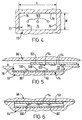
- the housing 70 has a rectangular recess 72 of a length l, and a width w and a depth d.
- the recess is defined by a planar floor 74, long parallel side walls 78 of length l and height d which are perpendicular to the floor and shorter parallel side walls 76 of length w and height d which are also perpendicular to the floor.
- the length l and width w of the recess are very slightly greater than the respective length and width of a SIM card 50, so that the SIM card can be dropped into the recess and fit there snugly.
- each of the SIM contacts 54 is positioned over a corresponding contact element 100.
- the SIM card is placed in the recess it is held in position by attaching the back cover of the phone as illustrated in Figures 5 and 6.
- the recess 72 in the housing 70 is defined by its side walls 78 and 76 and the floor 74.
- a planar layer of elastomeric material extends over the planar floor 74 of the recess 72.
- a planar substrate 90 of dielectric or insulating material is positioned on top of the elastomer 80 so that the upper surface of the dielectric is substantially parallel to the floor of the recess 72. .
- the substrate 90 has a plurality of contact elements 100 standing proud of the upper surface of the substrate each of which is electrically connected via an interconnect, on or within the substrate 90, to an input/output of the SIM card reader.
- Each protruding contact element is metallic and is preferably made of solid copper or solid copper with an overcoat of gold.
- the elements may have internal voids with are either empty or filled with material.
- the contact element has a wide base next to the upper surface of the substrate 90 and tapers to a point at a free end. The point can translate a moderate pressure supplied by the elastomer to the substrate in to a large force against the SIM card, he shape and size of the point affects the force. Thus the point of the contact can be dimensioned to penetrate a layer of oxide on the SIM card contact 54.
- the shape of contact element is preferably substantially pyramidal or conical, so that in cross-section the contact elements have a triangular cross-section. Typically the height of the contact element from base to point is about 0.1mm and the size of the base is about 0.4mm.
- the summation of the thickness of the elastomer layer 80 in its quiescent state, the thickness of the substrate 90 including the height of the contact elements 100, and the thickness of the SIM card 50 is greater than the depth d of the recess 72. Consequently when the SIM card is placed in the recess 72 it is supported by the contact elements 100 of the substrate 90 such that the SIM card does not lie wholly within the recess 72.
- attaching the back cover 66 to the phone body 64 having the card reader 2 presses the SIM card into the recess and clamps it there. Pressing the SIM card into the recess causes the elastomer layer to be resiliently compressed.
- the elastomer layer therefore in its compressed state provides a force which urges the contacts 100 of the reader 2 into physical contact with the contact portions 54 of the SIM card 50.
- the force of this urging may be controlled by selecting/varying the type elastomer material and the depth of the layer of elastomer material 80.
- SIM card 50 The placement of the SIM card 50 with the recess 72 and the attachment of the back cover are illustrated in Figures 5 and 6.
- the elastomer is in its quiescent state in Figure 5 and in its compressed state in Figure 6.
- SIM card is held in place by a drop-and-slide clamping system such in the Nokia 7110 (trademark), or a rotate-and-slide system as in the Nokia 6110 (trademark) or any other suitable system which clamps a SIM card within a recess.
- a drop-and-slide clamping system such in the Nokia 7110 (trademark), or a rotate-and-slide system as in the Nokia 6110 (trademark) or any other suitable system which clamps a SIM card within a recess.
- the substrate 90 with the plurality of pointed contact elements 100 is preferably manufactured in accordance with the process described in US 5,307,561 and US 5,354, 205 (the contents of which are hereby incorporated by reference). Such substrates are commercially available from Packard-Hughes Interconnect.
Landscapes
- Engineering & Computer Science (AREA)
- Artificial Intelligence (AREA)
- Computer Vision & Pattern Recognition (AREA)
- Physics & Mathematics (AREA)
- General Physics & Mathematics (AREA)
- Theoretical Computer Science (AREA)
- Computer Networks & Wireless Communication (AREA)
- Signal Processing (AREA)
- Telephone Set Structure (AREA)
- Coupling Device And Connection With Printed Circuit (AREA)
- Credit Cards Or The Like (AREA)
- Mobile Radio Communication Systems (AREA)
Abstract
Description
- The present invention relates to a card reader and in particular a card reader of reduced dimensions.
- Currently one of the drivers in the radio telephone market is phone size and it is desirable to reduce phone size. Over recent years there has been considerable success in reducing the length and width of a radio telephone. Although the depth of radio telephone has been reduced, it has been found that it is more difficult to reduce phone size in this dimension compared to other dimensions. This may result in aesthetically unappealing phone shapes.
- Accordingly it would be desirable to reduce the size of a radio telephone along its depth dimension.
- A typical radio telephone has a vast number of components. In the smaller radio telephones such as the NOKIA 8810 (Trade Mark) the phone has been carefully optimised to minimise weight and size. The innovation which underlies the present application results in part from the inventor's realisation that the SIM card reader, which is ostensibly optimally designed for space reduction, is one part of the radio telephone in which, with ingenuity, volume could be saved.
- Figures 1 and 2 illustrate a current
SIM card reader 2. TheSIM card reader 2 receives aSIM card 50 that has acard substrate 52 on which there is a plurality of separateconductive contact portions 54. Thereader 2 has aninterconnect 30 each of which connects acontact portion 54 of the SIM card to a radio telephone printedcircuit board 10 via aconnect 36. Theinterconnect 30 has a cantileveredportion 34 which is firmly held between anupper substrate 40 and alower substrate 20 of thecard reader 2 and acurved contact portion 32 for connecting with the acontact portion 54 of the SIM card. Thelower substrate 20 has arecess 22 position beneath thecurved contact portion 32 of theinterconnect 30. Thisrecess 22 has a clearance or depth 24. Theupper substrate 40 has a catch orclamp 42 which defines anabutting surface 44 which overhangs aparallel restraining portion 46 of theupper substrate 40. The gap between theabutting surface 44 of thecatch 42 and the restraining surface is slightly greater than the thickness of a SIM card. - The
SIM card 52 is placed into thecard reader 2 by lowering thecard 52 so that it abuts with thecurved contact portion 34 of theinterconnect 30 and flexes the interconnect and then sliding the card so that it nestles underneath theabutting surface 44. Releasing the card results in it being held between the upward force provided by theflexed interconnect 30 and the restraining reaction provided by theabutting surface 44. When the card is in position the cantileveredportion 34 of the interconnect is flexed downward and thecurved portion 32 moves into therecess 22. The cantilevering of theinterconnect 30 between therestraining portion 46 of the upper substrate and the lower substrate allows the resilient interconnect to return to its quiescent position standing proud of therestraining surface 46 when the card is removed. It is important that the SIM card can be easily removed and returned to the reader without any tools. - Further SIM card readers according to the prior art are described in US 5,718,609 and US 5,320,552.
- These SIM card readers also use resiliently flexible interconnects to connect to the SIM card. Such interconnects in SIM card readers are reliable and up until now there has been no motivation to adapt them.
- The inventor identified that the resiliently flexible interconnect provides the dual function of connecting the SIM card to the PCB and providing a sprung contact holding the SIM card in position. He realised that one feature limiting the reduction of the size of the card reader was that enough room must be provided in the SIM card reader to allow the
recess 22 to accept the resilient interconnect when it flexes downwards on inserting the SIM card. The inventor after having successfully identified where volume might be saved additionally realised how this saving may be effected by the novel application of known technology to provide both a low volume and reliable contact. - This known technology includes US 4,125,310, US 5, 197, 184 and US 5,364,277 which describe replacing the standard friction type connector which connects a flat cable to a circuit with a new type of two-part connector. A plurality of projecting interconnection features is provided on a first part of the connector. These projecting features are pressed against similar features or metallic connecting pads on a second part of the connector to form an electrical connection. The two connector parts are then physically clamped together ensuring the electrical contact between the two circuits. US 5,197,184 and US 5,364,277, in addition, relates to the additive electroforming of the plurality of projecting interconnection features. The circuit has an insulating substrate from which raised copper conductive elements protrude. The surface of the copper conductive elements is covered with gold. The techniques for forming and controlling the shape of the plurality of projecting interconnecting features are developed in US 5,307,561 and US 5,354,205. These documents describe how pyramidal and conical projecting features may be formed. The described connectors are available commercially from Packard-Hughes Interconnect under the trademark of "GoldDot".
- According to one aspect of the present invention there is provided a card reader comprising :
- a housing having a recess, having a substantially planar floor portion and wall portions,
- sized to accommodate and thereby position the card;
- resilient material within the recess and overlying at least portions of the recess floor;
- a dielectric substrate within the recess and supported by the resilient material, having an upper surface substantially planar to the floor of the recess and having contact elements extending from the substrate upper surface away from the recess floor wherein each contact element comprises a raised three dimensional metallic structure which extends substantially perpendicularly relative to the substrate upper surface, from a base portion at the substrate upper surface to a free end of reduced area; and
- means for holding the card within the recess while pressing the card toward the recess floor whereby the resilient material is compressed and physical connection is made between the card and the contact elements.
-
- According to another aspect of the present invention there is provided a radio communications device having a card reader comprising :
- a housing having a recess, having a substantially planar floor portion and wall portions,
- sized to accommodate and thereby position the card;
- resilient material within the recess and overlying at least portions of the recess floor;
- a dielectric substrate within the recess and supported by the resilient material, having an upper surface substantially planar to the floor of the recess and having contact elements extending from the substrate upper surface away from the recess floor wherein each contact element comprises a raised three dimensional metallic structure which extends substantially perpendicularly relative to the substrate upper surface, from a base portion at the substrate upper surface to a free end of reduced area; and
- means for holding the card within the recess while pressing the card toward the recess floor whereby the resilient material is compressed and physical connection is made between the card and the contact elements.
-
- The card reader is preferably a SIM card reader but may, for example, be a reader for other smart cards. The radio communications device is preferably a radio telephone but may, for example, be some other wireless device.
- The means for holding the SIM card may comprise a clamp by which the SIM card is urged into the recess or an attachable/detachable battery for the radio telephone by which the SIM card is urged into the recess when the battery is attached.
- The combined thickness of the SIM card, of the substrate including the extension of the contact elements, and of the resilient material in its quiescent state, preferably exceeds the depth dimension of the recess, whereby holding the SIM card within the recess compresses the resilient material and urges the SIM card and contact elements into physical contact. Preferably the resilient material has elastic properties and dimensions chosen to provide a suitable compressive force between SIM card and contact elements.
- Each contact element may taper from the base portion to the free end of reduced area. Furthermore, each contact element may be pointed at its free end to allow penetration of any oxide on the SIM card contacts. Each contact element may be shaped substantially as a pyramid or a cone. At least the surface of each contact element metallic and preferably the contact element is substantially solid copper or solid copper covered at least at the free end by gold.
- For a better understanding of the present invention reference will now be made by way of example only to the accompanying drawings in which:
- Figures 1 and 2 illustrate a current SIM card reader;
- Figure 3 illustrates a radio telephone;
- Figures 4, illustrates a SIM card reader according to the invention in plan view; and
- Figures 5 and 6 illustrate a SIM card reader according to the invention in cross-sectional view.
-
- One example of a
radio telephone 60 is illustrated in cross-section in Figure 3. The phone has afront cover 62 in which a user interface including adisplay 68 andkey pad 69 is defined, abody portion 64 containing the electronics of the phone and aback cover 66 which preferably contains a battery. Thebody 64 has aSIM card reader 2 containing aSIM card 50. TheSIM card reader 2 is accessible on removing theback cover 66 to remove or replace theSIM card 50 but is otherwise inaccessible. - Figures 4 and 5 illustrate a first embodiment of the present invention. A
card reader 2 has a body orhousing 70, which may or may not be an integral part of thephone body 64. Thehousing 70 has arectangular recess 72 of a length l, and a width w and a depth d. The recess is defined by aplanar floor 74, longparallel side walls 78 of length l and height d which are perpendicular to the floor and shorterparallel side walls 76 of length w and height d which are also perpendicular to the floor. The length l and width w of the recess are very slightly greater than the respective length and width of aSIM card 50, so that the SIM card can be dropped into the recess and fit there snugly. Exposed within the recess are pluralities ofcontact elements 100, which physically connect to thecontact areas 54 on a SIM card when, fitted into the recess. The snug fit of the SIM card to the recess ensures that each of theSIM contacts 54 is positioned over acorresponding contact element 100. When the SIM card is placed in the recess it is held in position by attaching the back cover of the phone as illustrated in Figures 5 and 6. - Referring to Figure 5, a cross-section of the SIM card holder is illustrated. The
recess 72 in thehousing 70 is defined by itsside walls floor 74. A planar layer of elastomeric material extends over theplanar floor 74 of therecess 72. Aplanar substrate 90 of dielectric or insulating material is positioned on top of theelastomer 80 so that the upper surface of the dielectric is substantially parallel to the floor of therecess 72. . Thesubstrate 90 has a plurality ofcontact elements 100 standing proud of the upper surface of the substrate each of which is electrically connected via an interconnect, on or within thesubstrate 90, to an input/output of the SIM card reader. - Each protruding contact element is metallic and is preferably made of solid copper or solid copper with an overcoat of gold. The elements may have internal voids with are either empty or filled with material. The contact element has a wide base next to the upper surface of the
substrate 90 and tapers to a point at a free end. The point can translate a moderate pressure supplied by the elastomer to the substrate in to a large force against the SIM card, he shape and size of the point affects the force. Thus the point of the contact can be dimensioned to penetrate a layer of oxide on the SIM card contact 54.The shape of contact element is preferably substantially pyramidal or conical, so that in cross-section the contact elements have a triangular cross-section. Typically the height of the contact element from base to point is about 0.1mm and the size of the base is about 0.4mm. - The summation of the thickness of the
elastomer layer 80 in its quiescent state, the thickness of thesubstrate 90 including the height of thecontact elements 100, and the thickness of theSIM card 50 is greater than the depth d of therecess 72. Consequently when the SIM card is placed in therecess 72 it is supported by thecontact elements 100 of thesubstrate 90 such that the SIM card does not lie wholly within therecess 72. However, attaching theback cover 66 to thephone body 64 having thecard reader 2 presses the SIM card into the recess and clamps it there. Pressing the SIM card into the recess causes the elastomer layer to be resiliently compressed. The elastomer layer therefore in its compressed state provides a force which urges thecontacts 100 of thereader 2 into physical contact with thecontact portions 54 of theSIM card 50. The force of this urging may be controlled by selecting/varying the type elastomer material and the depth of the layer ofelastomer material 80. - The placement of the
SIM card 50 with therecess 72 and the attachment of the back cover are illustrated in Figures 5 and 6. The elastomer is in its quiescent state in Figure 5 and in its compressed state in Figure 6. - Other embodiments of the invention are possible in which the SIM card is held in place by a drop-and-slide clamping system such in the Nokia 7110 (trademark), or a rotate-and-slide system as in the Nokia 6110 (trademark) or any other suitable system which clamps a SIM card within a recess.
- The
substrate 90 with the plurality ofpointed contact elements 100 is preferably manufactured in accordance with the process described in US 5,307,561 and US 5,354, 205 (the contents of which are hereby incorporated by reference). Such substrates are commercially available from Packard-Hughes Interconnect.
Claims (13)
- A card reader comprising :a housing having a recess, having a substantially planar floor portion and wall portions,sized to accommodate and thereby position the card;resilient material within the recess and overlying at least portions of the recess floor;a dielectric substrate within the recess and supported by the resilient material, having an upper surface substantially planar to the floor of the recess and having contact elements extending from the substrate upper surface away from the recess floor wherein each contact element comprises a raised three dimensional metallic structure which extends substantially perpendicularly relative to the substrate upper surface, from a base portion at the substrate upper surface to a free end of reduced area; andmeans for holding the card within the recess while pressing the card toward the recess floor whereby the resilient material is compressed and physical connection is made between the card and the contact elements.
- A radio communications device having a card reader comprising :a housing having a recess, having a substantially planar floor portion and wall portions,sized to accommodate and thereby position the card;resilient material within the recess and overlying at least portions of the recess floor;a dielectric substrate within the recess and supported by the resilient material, having an upper surface substantially planar to the floor of the recess and having contact elements extending from the substrate upper surface away from the recess floor wherein each contact element comprises a raised three dimensional metallic structure which extends substantially perpendicularly relative to the substrate upper surface, from a base portion at the substrate upper surface to a free end of reduced area; andmeans for holding the card within the recess while pressing the card toward the recess floor whereby the resilient material is compressed and physical connection is made between the card and the contact elements.
- A card reader or a radio communications device as claimed in any preceding claim, wherein the means for holding the card comprises a clamp by which the card is urged into the recess.
- A radio communications device as claimed in claim 2, wherein the means for holding the card comprises an attachable/detachable battery for the radio communications device by which the card is urged into the recess when the battery is attached.
- A card reader or a radio communications device as claimed in any preceding claim wherein the combined thickness of the card, of the substrate including the extension of the contact elements, and of the resilient material in its quiescent state, exceeds the depth dimension of the recess, whereby holding the card within the recess compresses the resilient material and urgess the card and contact elements into physical contact.
- A card reader or a radio communications device as claimed in claim 5, wherein the resilient material has elastic properties and dimensions chosen to provide a suitable compressive force between card and contact elements.
- A card reader or a radio communications device as claimed in any preceding claim wherein each contact element tapers from the base portion to the free end of reduced area.
- A card reader or a radio communications device as claimed in any preceding claim wherein each contact element is pointed at its free end to allow penetration of any oxide on the card contacts
- A card reader or a radio communications device as claimed in any claim wherein each contact element is shaped substantially as a pyramid or a cone.
- A card reader or a radio communications device as claimed in any claim wherein at least the surface of each contact element is metallic.
- A card reader or a radio communications device as claimed in any claim wherein the contact element comprises copper.
- A card reader or a radio communications device as claimed in any claim wherein the contact element comprises copper covered at least at the free end by gold.
- A card reader or a radio communications device as claimed in any claim wherein the dielectric substrate and its contact elements are made in accordance with a method described in any one of the patents within a patent family including the patent US 4,125,310 or US 5,354,205 or US 5,307,561 or US 5,197,184 or US 5,364,277.
Applications Claiming Priority (2)
| Application Number | Priority Date | Filing Date | Title |
|---|---|---|---|
| GB9916908A GB2352315B (en) | 1999-07-19 | 1999-07-19 | Sim card reader |
| GB9916908 | 1999-07-19 |
Publications (3)
| Publication Number | Publication Date |
|---|---|
| EP1071032A2 true EP1071032A2 (en) | 2001-01-24 |
| EP1071032A3 EP1071032A3 (en) | 2002-09-04 |
| EP1071032B1 EP1071032B1 (en) | 2013-02-20 |
Family
ID=10857512
Family Applications (1)
| Application Number | Title | Priority Date | Filing Date |
|---|---|---|---|
| EP00304930A Expired - Lifetime EP1071032B1 (en) | 1999-07-19 | 2000-06-09 | A card reader |
Country Status (4)
| Country | Link |
|---|---|
| US (1) | US6325637B1 (en) |
| EP (1) | EP1071032B1 (en) |
| JP (1) | JP2001102114A (en) |
| GB (1) | GB2352315B (en) |
Cited By (2)
| Publication number | Priority date | Publication date | Assignee | Title |
|---|---|---|---|---|
| WO2002071314A1 (en) * | 2001-03-05 | 2002-09-12 | Activcard Ireland, Limited | Method and system for adaptively varying templates to accommodate changes in biometric information |
| KR100497402B1 (en) * | 2001-04-10 | 2005-06-23 | 주식회사 팬택앤큐리텔 | Cellular phone for having uim card |
Families Citing this family (3)
| Publication number | Priority date | Publication date | Assignee | Title |
|---|---|---|---|---|
| US6831977B2 (en) * | 2001-02-23 | 2004-12-14 | Molex Incorporated | Cover for a telephone handset |
| TW562361U (en) * | 2002-12-31 | 2003-11-11 | Hon Hai Prec Ind Co Ltd | Mechanism for holding SIM card |
| JP2008504627A (en) * | 2004-06-30 | 2008-02-14 | コーニンクレッカ フィリップス エレクトロニクス エヌ ヴィ | Chip card for holder insertion |
Citations (5)
| Publication number | Priority date | Publication date | Assignee | Title |
|---|---|---|---|---|
| US4125310A (en) | 1975-12-01 | 1978-11-14 | Hughes Aircraft Co | Electrical connector assembly utilizing wafers for connecting electrical cables |
| US5197184A (en) | 1990-09-11 | 1993-03-30 | Hughes Aircraft Company | Method of forming three-dimensional circuitry |
| US5307561A (en) | 1991-08-26 | 1994-05-03 | Hughes Aircraft Company | Method for making 3-D electrical circuitry |
| US5364277A (en) | 1990-09-11 | 1994-11-15 | Hughes Aircraft Company | Three-dimensional electroformed circuitry |
| DE19733425A1 (en) | 1997-08-01 | 1999-02-04 | Bosch Gmbh Robert | Device for reading information carrier cards |
Family Cites Families (22)
| Publication number | Priority date | Publication date | Assignee | Title |
|---|---|---|---|---|
| GB2136212B (en) * | 1983-01-06 | 1986-10-15 | Welwyn Electronics Ltd | Cooling components on printed circuit boards |
| US4927368A (en) * | 1986-10-13 | 1990-05-22 | Sharp Kabushiki Kaisha | Connector |
| JPH01134366U (en) * | 1988-03-07 | 1989-09-13 | ||
| US5726432A (en) * | 1993-05-14 | 1998-03-10 | Amphenol-Tuchel Electronics Gmbh | Contacting system or reader for chip cards |
| JP2867209B2 (en) * | 1993-08-27 | 1999-03-08 | 日東電工株式会社 | Method of connecting flexible circuit board to contact object and structure thereof |
| US5661634A (en) * | 1993-11-09 | 1997-08-26 | Fujitsu Limited | Information processing system using portable terminal unit and data communication adapter therefor |
| US5468917A (en) * | 1994-03-23 | 1995-11-21 | International Business Machines Corporation | Circuitized structure including flexible circuit with elastomeric member bonded thereto |
| FI944109L (en) * | 1994-09-07 | 1996-03-08 | Nokia Mobile Phones Ltd | Arrangement for securing a mobile phone SIM card |
| DE19516987A1 (en) * | 1995-05-09 | 1996-11-14 | Amphenol Tuchel Elect | Card reading device for chip cards and / or SIM cards with different thickness |
| US5772488A (en) * | 1995-10-16 | 1998-06-30 | Micron Display Technology, Inc. | Method of forming a doped field emitter array |
| FR2747847B1 (en) * | 1996-04-18 | 1998-07-03 | Itt Composants Instr | ELECTRONIC CONNECTION BOX, TO A PERSONAL COMPUTER, EQUIPPED WITH A CONNECTOR FOR A CHIP CARD |
| EP0833271A3 (en) * | 1996-09-20 | 1998-06-17 | Siemens Aktiengesellschaft | Chipcard reader |
| DE29718773U1 (en) * | 1997-10-22 | 1997-12-04 | Stocko Metallwarenfabriken Henkels & Sohn GmbH & Co, 42327 Wuppertal | Chip card contact unit |
| US5899757A (en) * | 1997-11-03 | 1999-05-04 | Intercon Systems, Inc. | Compression connector |
| US6114221A (en) * | 1998-03-16 | 2000-09-05 | International Business Machines Corporation | Method and apparatus for interconnecting multiple circuit chips |
| DE19846366C2 (en) * | 1998-04-07 | 2000-07-27 | Itt Mfg Enterprises Inc | Plug-in card for electronic devices |
| EP0951161A1 (en) * | 1998-04-16 | 1999-10-20 | Koninklijke Philips Electronics N.V. | Contact device for connecting a liquid crystal display to a printed circuit board |
| JPH11329648A (en) * | 1998-05-19 | 1999-11-30 | Molex Inc | IC device socket |
| US6173405B1 (en) * | 1998-05-29 | 2001-01-09 | 3Com Corporation | Secure communications card modem and method of using same |
| US6062887A (en) * | 1998-08-31 | 2000-05-16 | Motorola, Inc. | Electronic device with dual card reader employing a drawer |
| US6164979A (en) * | 1999-03-12 | 2000-12-26 | Motorola, Inc. | System for providing a removable high density electrical interconnect for flexible circuits |
| US6164984A (en) * | 1999-04-01 | 2000-12-26 | Schreiner Etiketten Und Selbstkelbetechnik Gmbh & Co. | Electrical connecting element |
-
1999
- 1999-07-19 GB GB9916908A patent/GB2352315B/en not_active Expired - Fee Related
-
2000
- 2000-06-09 EP EP00304930A patent/EP1071032B1/en not_active Expired - Lifetime
- 2000-07-18 JP JP2000216843A patent/JP2001102114A/en active Pending
- 2000-07-19 US US09/619,657 patent/US6325637B1/en not_active Expired - Fee Related
Patent Citations (6)
| Publication number | Priority date | Publication date | Assignee | Title |
|---|---|---|---|---|
| US4125310A (en) | 1975-12-01 | 1978-11-14 | Hughes Aircraft Co | Electrical connector assembly utilizing wafers for connecting electrical cables |
| US5197184A (en) | 1990-09-11 | 1993-03-30 | Hughes Aircraft Company | Method of forming three-dimensional circuitry |
| US5364277A (en) | 1990-09-11 | 1994-11-15 | Hughes Aircraft Company | Three-dimensional electroformed circuitry |
| US5307561A (en) | 1991-08-26 | 1994-05-03 | Hughes Aircraft Company | Method for making 3-D electrical circuitry |
| US5354205A (en) | 1991-08-26 | 1994-10-11 | Hughes Aircraft Company | Electrical connections with shaped contacts |
| DE19733425A1 (en) | 1997-08-01 | 1999-02-04 | Bosch Gmbh Robert | Device for reading information carrier cards |
Cited By (4)
| Publication number | Priority date | Publication date | Assignee | Title |
|---|---|---|---|---|
| WO2002071314A1 (en) * | 2001-03-05 | 2002-09-12 | Activcard Ireland, Limited | Method and system for adaptively varying templates to accommodate changes in biometric information |
| US7103200B2 (en) | 2001-03-05 | 2006-09-05 | Robert Hillhouse | Method and system for adaptively varying templates to accommodate changes in biometric information |
| US7372979B2 (en) | 2001-03-05 | 2008-05-13 | Activcard Ireland Limited | Method and system for adaptively varying templates to accommodate changes in biometric information |
| KR100497402B1 (en) * | 2001-04-10 | 2005-06-23 | 주식회사 팬택앤큐리텔 | Cellular phone for having uim card |
Also Published As
| Publication number | Publication date |
|---|---|
| EP1071032A3 (en) | 2002-09-04 |
| GB2352315B (en) | 2003-12-03 |
| GB2352315A (en) | 2001-01-24 |
| EP1071032B1 (en) | 2013-02-20 |
| GB9916908D0 (en) | 1999-09-22 |
| JP2001102114A (en) | 2001-04-13 |
| US6325637B1 (en) | 2001-12-04 |
Similar Documents
| Publication | Publication Date | Title |
|---|---|---|
| CN201556744U (en) | SIM card installation device for portable terminal | |
| US5823828A (en) | Smart card connector with slidable cover | |
| TW421899B (en) | Very thin electrical connector for connecting a smart card | |
| CN1574494B (en) | Electrical connector assembly, receptacle connector and plug connector | |
| EP0905827A3 (en) | Improved chip card connector | |
| CN1234127A (en) | Subscriber Identity Module (SIM) Card Holder | |
| EP1331595A3 (en) | Connector device for cards permitting insertion of different types of cards | |
| US6842336B2 (en) | Portable electronic device with carrier plate | |
| EP0967771A3 (en) | Sim card terminal | |
| US6855004B2 (en) | Electrostatic protection cover | |
| JP2002289295A (en) | Card connector | |
| EP1160931A3 (en) | Card connector device | |
| EP0984518A3 (en) | Electrical connector for PGA package | |
| GB2330009A (en) | Electrically connecting a component to a PCB using a compression spring | |
| US7354290B2 (en) | Surface contact card holder | |
| EP1071032B1 (en) | A card reader | |
| US6033234A (en) | Printed circuit board to flexible printed circuit connection system | |
| US20090137136A1 (en) | Housing, Terminal and Connector Using Housing and Terminal | |
| US6224388B1 (en) | In-board connector | |
| EP1143371A3 (en) | Electrical connector | |
| EP1309039A3 (en) | Ball grid array socket | |
| EP0901187A3 (en) | Connector for Connecting a printed circuit board to a flat flexible circuit | |
| EP1304767A3 (en) | Flexible circuit board connecting device | |
| US6796842B1 (en) | Electronic card connector | |
| US20220140510A1 (en) | Card retaining member and card connector set |
Legal Events
| Date | Code | Title | Description |
|---|---|---|---|
| PUAI | Public reference made under article 153(3) epc to a published international application that has entered the european phase |
Free format text: ORIGINAL CODE: 0009012 |
|
| AK | Designated contracting states |
Kind code of ref document: A2 Designated state(s): AT BE CH CY DE DK ES FI FR GB GR IE IT LI LU MC NL PT SE |
|
| AX | Request for extension of the european patent |
Free format text: AL;LT;LV;MK;RO;SI |
|
| RAP1 | Party data changed (applicant data changed or rights of an application transferred) |
Owner name: NOKIA CORPORATION |
|
| PUAL | Search report despatched |
Free format text: ORIGINAL CODE: 0009013 |
|
| AK | Designated contracting states |
Kind code of ref document: A3 Designated state(s): AT BE CH CY DE DK ES FI FR GB GR IE IT LI LU MC NL PT SE |
|
| AX | Request for extension of the european patent |
Free format text: AL;LT;LV;MK;RO;SI |
|
| 17P | Request for examination filed |
Effective date: 20030304 |
|
| AKX | Designation fees paid |
Designated state(s): DE FR GB IT |
|
| 17Q | First examination report despatched |
Effective date: 20091015 |
|
| GRAP | Despatch of communication of intention to grant a patent |
Free format text: ORIGINAL CODE: EPIDOSNIGR1 |
|
| GRAJ | Information related to disapproval of communication of intention to grant by the applicant or resumption of examination proceedings by the epo deleted |
Free format text: ORIGINAL CODE: EPIDOSDIGR1 |
|
| GRAP | Despatch of communication of intention to grant a patent |
Free format text: ORIGINAL CODE: EPIDOSNIGR1 |
|
| GRAS | Grant fee paid |
Free format text: ORIGINAL CODE: EPIDOSNIGR3 |
|
| GRAA | (expected) grant |
Free format text: ORIGINAL CODE: 0009210 |
|
| AK | Designated contracting states |
Kind code of ref document: B1 Designated state(s): DE FR GB IT |
|
| REG | Reference to a national code |
Ref country code: GB Ref legal event code: FG4D |
|
| REG | Reference to a national code |
Ref country code: DE Ref legal event code: R096 Ref document number: 60047837 Country of ref document: DE Effective date: 20130418 |
|
| PLBE | No opposition filed within time limit |
Free format text: ORIGINAL CODE: 0009261 |
|
| STAA | Information on the status of an ep patent application or granted ep patent |
Free format text: STATUS: NO OPPOSITION FILED WITHIN TIME LIMIT |
|
| PG25 | Lapsed in a contracting state [announced via postgrant information from national office to epo] |
Ref country code: IT Free format text: LAPSE BECAUSE OF FAILURE TO SUBMIT A TRANSLATION OF THE DESCRIPTION OR TO PAY THE FEE WITHIN THE PRESCRIBED TIME-LIMIT Effective date: 20130220 |
|
| 26N | No opposition filed |
Effective date: 20131121 |
|
| GBPC | Gb: european patent ceased through non-payment of renewal fee |
Effective date: 20130609 |
|
| REG | Reference to a national code |
Ref country code: DE Ref legal event code: R097 Ref document number: 60047837 Country of ref document: DE Effective date: 20131121 |
|
| REG | Reference to a national code |
Ref country code: DE Ref legal event code: R119 Ref document number: 60047837 Country of ref document: DE Effective date: 20140101 |
|
| REG | Reference to a national code |
Ref country code: FR Ref legal event code: ST Effective date: 20140228 |
|
| PG25 | Lapsed in a contracting state [announced via postgrant information from national office to epo] |
Ref country code: DE Free format text: LAPSE BECAUSE OF NON-PAYMENT OF DUE FEES Effective date: 20140101 Ref country code: GB Free format text: LAPSE BECAUSE OF NON-PAYMENT OF DUE FEES Effective date: 20130609 |
|
| PG25 | Lapsed in a contracting state [announced via postgrant information from national office to epo] |
Ref country code: FR Free format text: LAPSE BECAUSE OF NON-PAYMENT OF DUE FEES Effective date: 20130701 |